EP0262346A1 - Diode IMPATT - Google Patents
Diode IMPATT Download PDFInfo
- Publication number
- EP0262346A1 EP0262346A1 EP87111422A EP87111422A EP0262346A1 EP 0262346 A1 EP0262346 A1 EP 0262346A1 EP 87111422 A EP87111422 A EP 87111422A EP 87111422 A EP87111422 A EP 87111422A EP 0262346 A1 EP0262346 A1 EP 0262346A1
- Authority
- EP
- European Patent Office
- Prior art keywords
- layer
- impatt diode
- sige
- doped
- impatt
- Prior art date
- Legal status (The legal status is an assumption and is not a legal conclusion. Google has not performed a legal analysis and makes no representation as to the accuracy of the status listed.)
- Granted
Links
- 229910000577 Silicon-germanium Inorganic materials 0.000 claims abstract description 34
- 239000000758 substrate Substances 0.000 claims abstract description 11
- 239000004065 semiconductor Substances 0.000 claims description 18
- 239000000463 material Substances 0.000 claims description 4
- 238000000034 method Methods 0.000 claims description 2
- 238000001451 molecular beam epitaxy Methods 0.000 claims description 2
- 229910021419 crystalline silicon Inorganic materials 0.000 claims 1
- 239000010410 layer Substances 0.000 description 42
- 239000002356 single layer Substances 0.000 description 6
- 239000002800 charge carrier Substances 0.000 description 5
- 230000000903 blocking effect Effects 0.000 description 2
- 230000015556 catabolic process Effects 0.000 description 2
- 238000010586 diagram Methods 0.000 description 2
- 229910052782 aluminium Inorganic materials 0.000 description 1
- 229910052787 antimony Inorganic materials 0.000 description 1
- 229910052785 arsenic Inorganic materials 0.000 description 1
- 229910052796 boron Inorganic materials 0.000 description 1
- 239000013078 crystal Substances 0.000 description 1
- 238000011161 development Methods 0.000 description 1
- 230000018109 developmental process Effects 0.000 description 1
- 229910052733 gallium Inorganic materials 0.000 description 1
- 229910052738 indium Inorganic materials 0.000 description 1
- 230000007246 mechanism Effects 0.000 description 1
- 229910021421 monocrystalline silicon Inorganic materials 0.000 description 1
- 229910052698 phosphorus Inorganic materials 0.000 description 1
Images
Classifications
-
- H—ELECTRICITY
- H01—ELECTRIC ELEMENTS
- H01L—SEMICONDUCTOR DEVICES NOT COVERED BY CLASS H10
- H01L29/00—Semiconductor devices adapted for rectifying, amplifying, oscillating or switching, or capacitors or resistors with at least one potential-jump barrier or surface barrier, e.g. PN junction depletion layer or carrier concentration layer; Details of semiconductor bodies or of electrodes thereof ; Multistep manufacturing processes therefor
- H01L29/02—Semiconductor bodies ; Multistep manufacturing processes therefor
- H01L29/12—Semiconductor bodies ; Multistep manufacturing processes therefor characterised by the materials of which they are formed
- H01L29/16—Semiconductor bodies ; Multistep manufacturing processes therefor characterised by the materials of which they are formed including, apart from doping materials or other impurities, only elements of Group IV of the Periodic System
- H01L29/161—Semiconductor bodies ; Multistep manufacturing processes therefor characterised by the materials of which they are formed including, apart from doping materials or other impurities, only elements of Group IV of the Periodic System including two or more of the elements provided for in group H01L29/16, e.g. alloys
- H01L29/165—Semiconductor bodies ; Multistep manufacturing processes therefor characterised by the materials of which they are formed including, apart from doping materials or other impurities, only elements of Group IV of the Periodic System including two or more of the elements provided for in group H01L29/16, e.g. alloys in different semiconductor regions, e.g. heterojunctions
-
- H—ELECTRICITY
- H01—ELECTRIC ELEMENTS
- H01L—SEMICONDUCTOR DEVICES NOT COVERED BY CLASS H10
- H01L29/00—Semiconductor devices adapted for rectifying, amplifying, oscillating or switching, or capacitors or resistors with at least one potential-jump barrier or surface barrier, e.g. PN junction depletion layer or carrier concentration layer; Details of semiconductor bodies or of electrodes thereof ; Multistep manufacturing processes therefor
- H01L29/66—Types of semiconductor device ; Multistep manufacturing processes therefor
- H01L29/86—Types of semiconductor device ; Multistep manufacturing processes therefor controllable only by variation of the electric current supplied, or only the electric potential applied, to one or more of the electrodes carrying the current to be rectified, amplified, oscillated or switched
- H01L29/861—Diodes
- H01L29/864—Transit-time diodes, e.g. IMPATT, TRAPATT diodes
Definitions
- the invention relates to an IMPATT diode according to the preamble of patent claim 1.
- IMPATT diodes are powerful millimeter wave components. They are used in particular to generate vibrations.
- a structure suitable for generating and combining these mechanisms is, for example, a pn junction.
- the voltage required for the avalanche breakdown of the IMPATT diode can be reduced by using a heterojunction instead of a p-n junction.
- the heterostructure of the IMPATT diode must be constructed in such a way that the semiconductor material of the generation zone (avalanche breakdown zone) has a smaller band gap than that of the drift zone. This lowers the ionization threshold energy and thus increases the efficiency of the IMPATT diode.
- the invention is therefore based on the object of specifying an IMPATT diode with a heterostructure which can be produced economically, which has a high degree of efficiency and whose wavelength range encompasses the mm and sub-mm range.
- the invention has the advantage that the IMPATT diode is made with an inexpensive Si substrate and you Efficiency is improved by a suitable Si / SiGe heterostructure.
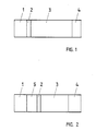
- n+-doped Si substrate 1 is a semiconductor layer sequence on a p+-doped Si substrate 1 with a charge carrier concentration of more than 101 nie cm ⁇ 3 an undoped SiGe layer 2 with a layer thickness of approximately 0.02 ⁇ m, an n-doped Si layer 3 with a charge carrier concentration of approximately 1.4 ⁇ 1017 cm ⁇ 3 and a layer thickness of approximately 0.3 ⁇ m, - An n+-doped Si layer with a charge carrier concentration of about 5 ⁇ 1019 cm ⁇ 3 and a layer thickness of about 0.1 microns applied.
- Doping materials for the n-doping are, for example, Sb, P, As and for the p-doping B, Ga, Al, In.
- a so high blocking voltage is applied to the structure according to FIG. 1 that the blocking layer extends over the semiconductor layers 2, 3.
- the maximum field strength is so great that impact ionization sets in.
- the semiconductor layer structure of an IMPATT diode according to FIG. 1 differs from an Si-based IMPATT diode with a pn junction in that an SiGe layer 2 has been grown at the point where it is required for impact ionization and thus for avalanche multiplication Field strength occurs.
- E g 0.76 eV.
- the different lattice constants of Si and SiGe generate a lateral mechanical stress in the semiconductor layers. If, for example, an Si 0.6 Ge 0.4 layer 2 with a subcritical layer thickness of approximately 0.02 ⁇ m is deposited on an Si substrate 1, a lateral compressive stress arises in the SiGe layer, since the natural lattice constant of single-crystal SiGe is larger than that of single crystal Si. A layer thickness is called subcritical if the layers consisting of different semiconductor materials have the same lattice constant in the lateral direction. There is then a pseudomorphic growth. The compressive stress compresses the SiGe layer by up to 4%. The mechanical tension resulting from the pseudomorphic growth leads to a reduction in the band distance from SiGe and causes an additional reduction in the ionization threshold energy of SiGe.
- an IMPATT diode with a double heterostructure is specified.
- the double heterostructure differs, for example, from the single heterostructure (FIG. 1) in that it has a further p-doped Si layer 5 that has been grown between the p+-doped substrate 1 and the undoped SiGe layer 2 (FIG. 2).
- the Si layer 5 has a layer thickness of approximately 0.25 ⁇ m and a positive charge carrier concentration of approximately 1.6. 1017 cm ⁇ 3.
- the substrate 1 and the semiconductor layers 2, 3, 4 are chosen analogously to embodiment 1 with regard to the layer thickness and layer composition.
- the mechanical stress in the SiGe layer caused by the different lattice constant of Si and SiGe advantageously brings about a reduction in the bandgap in the SiGe layer and a lowering of the ionization threshold energy.
- the higher ionization rate of SiGe has the advantage that the spatial area in which power dissipation occurs is reduced and the efficiency of the IMPATT diode is increased.
- the efficiency of the heterostructure IMPATT diodes according to the invention is between 12 and 15% for a frequency of 100 GHz.
- the Ge fraction x in the Si 1-x Ge x layers of the superlattice can be chosen larger than in a corresponding Si 1-x Ge with the same layer thickness as for a SiGe single layer x single layer.
- the Band gap to conduction band E c is smaller than the band distance between valence and conduction band of a SiGe single layer with the same layer thickness.
- all of the individual layers of the superlattice have the same layer thickness.
- the critical layer thickness of the Si / Si 1-x Ge x superlattice is greater for the same Ge component x than for a Si 1-x Ge x single layer.
- the layer thickness of the generation zone can be selected to be larger when using an Si / SiGe superlattice than for an SiGe single layer. This has the advantage that the superlattice IMPATT diode can be used over a wider frequency range than the corresponding heterostructure IMPATT diode with only one SiGe layer.
- the wavelength range of the IMPATT diodes according to the invention is in the mm and sub-mm range.
- heterostructure semiconductor layer sequences of the IMPATT diodes according to the invention are produced using the molecular beam epitaxy method.
- the invention is not limited to the specified p+inn+ or p+pinn+ structure of the IMPATT diodes, but can also be applied to the inverse structures which result from the fact that the conductivity type of the semiconductor layers is interchanged in the exemplary embodiments ( n line is replaced by p line and vice versa). Furthermore, not only the specified quasi-read structures are suitable for the IMPATT diodes according to the invention, but the invention can also be used for Misawa diodes.
Landscapes
- Engineering & Computer Science (AREA)
- Microelectronics & Electronic Packaging (AREA)
- Power Engineering (AREA)
- Physics & Mathematics (AREA)
- Ceramic Engineering (AREA)
- Condensed Matter Physics & Semiconductors (AREA)
- General Physics & Mathematics (AREA)
- Computer Hardware Design (AREA)
- Bipolar Transistors (AREA)
- Electrodes Of Semiconductors (AREA)
- Recrystallisation Techniques (AREA)
Applications Claiming Priority (4)
| Application Number | Priority Date | Filing Date | Title |
|---|---|---|---|
| DE3632921 | 1986-09-27 | ||
| DE3632921 | 1986-09-27 | ||
| DE19873725214 DE3725214A1 (de) | 1986-09-27 | 1987-07-30 | Impatt-diode |
| DE3725214 | 1987-07-30 |
Publications (2)
| Publication Number | Publication Date |
|---|---|
| EP0262346A1 true EP0262346A1 (fr) | 1988-04-06 |
| EP0262346B1 EP0262346B1 (fr) | 1993-03-31 |
Family
ID=25847918
Family Applications (1)
| Application Number | Title | Priority Date | Filing Date |
|---|---|---|---|
| EP87111422A Expired - Lifetime EP0262346B1 (fr) | 1986-09-27 | 1987-08-07 | Diode IMPATT |
Country Status (3)
| Country | Link |
|---|---|
| US (1) | US4857972A (fr) |
| EP (1) | EP0262346B1 (fr) |
| DE (2) | DE3725214A1 (fr) |
Cited By (2)
| Publication number | Priority date | Publication date | Assignee | Title |
|---|---|---|---|---|
| EP0593982A2 (fr) * | 1992-10-20 | 1994-04-27 | Daimler-Benz Aktiengesellschaft | Diode BARITT en Si/SiGe |
| WO2000025366A1 (fr) * | 1998-10-23 | 2000-05-04 | The Secretary Of State For Defence | Amelioration de diodes impatt |
Families Citing this family (12)
| Publication number | Priority date | Publication date | Assignee | Title |
|---|---|---|---|---|
| DE3937329B4 (de) * | 1989-11-09 | 2004-10-14 | Atmel Germany Gmbh | Halbleiter-Bauelement und seine Verwendung |
| US5168328A (en) * | 1990-07-03 | 1992-12-01 | Litton Systems, Inc. | Heterojunction impatt diode |
| US5466965A (en) * | 1992-12-02 | 1995-11-14 | The Regents Of The University Of California | High efficiency, high power multiquantum well IMPATT device with optical injection locking |
| DE4319211B4 (de) * | 1993-06-09 | 2004-04-15 | Daimlerchrysler Ag | Tunnel-BARITT-Diode |
| US5685946A (en) * | 1993-08-11 | 1997-11-11 | The United States Of America As Represented By The Administrator Of The National Aeronautics And Space Administration | Method of producing buried porous silicon-geramanium layers in monocrystalline silicon lattices |
| US5550387A (en) * | 1994-01-24 | 1996-08-27 | Hi-Z Corporation | Superlattice quantum well material |
| DE19713962C1 (de) * | 1997-04-04 | 1998-07-02 | Siemens Ag | Leistungsdiode (FCI-Diode) |
| US6074960A (en) | 1997-08-20 | 2000-06-13 | Micron Technology, Inc. | Method and composition for selectively etching against cobalt silicide |
| DE19956903B4 (de) * | 1999-11-26 | 2009-04-09 | United Monolithic Semiconductors Gmbh | HF-Halbleiterbauelement und Verfahren zur Integration von HF-Dioden |
| CN1309094C (zh) * | 2004-03-17 | 2007-04-04 | 清华大学 | 基于Si/SiGe的空穴型共振隧穿二极管 |
| JP2013004541A (ja) * | 2011-06-10 | 2013-01-07 | Toshiba Corp | 半導体記憶装置 |
| US9412879B2 (en) | 2013-07-18 | 2016-08-09 | Texas Instruments Incorporated | Integration of the silicon IMPATT diode in an analog technology |
Citations (4)
| Publication number | Priority date | Publication date | Assignee | Title |
|---|---|---|---|---|
| US3466312A (en) * | 1964-06-08 | 1969-09-09 | Robins Co Inc A H | Derivatives of dialkyl-cysteines and allied compounds |
| FR2225842A1 (fr) * | 1973-04-13 | 1974-11-08 | Thomson Csf | |
| US4291320A (en) * | 1980-01-10 | 1981-09-22 | Rockwell International Corporation | Heterojunction IMPATT diode |
| US4529455A (en) * | 1983-10-28 | 1985-07-16 | At&T Bell Laboratories | Method for epitaxially growing Gex Si1-x layers on Si utilizing molecular beam epitaxy |
Family Cites Families (3)
| Publication number | Priority date | Publication date | Assignee | Title |
|---|---|---|---|---|
| US3466512A (en) * | 1967-05-29 | 1969-09-09 | Bell Telephone Labor Inc | Impact avalanche transit time diodes with heterojunction structure |
| FR2379169A1 (fr) * | 1977-01-28 | 1978-08-25 | Thomson Csf | Diode a avalanche constituee par une hetero-jonction et oscillateur en mode dit " a temps de transit " comportant une telle diode |
| US4257055A (en) * | 1979-07-26 | 1981-03-17 | University Of Illinois Foundation | Negative resistance heterojunction devices |
-
1987
- 1987-07-30 DE DE19873725214 patent/DE3725214A1/de not_active Withdrawn
- 1987-08-07 EP EP87111422A patent/EP0262346B1/fr not_active Expired - Lifetime
- 1987-08-07 DE DE8787111422T patent/DE3785126D1/de not_active Expired - Fee Related
- 1987-09-28 US US07/105,952 patent/US4857972A/en not_active Expired - Lifetime
Patent Citations (4)
| Publication number | Priority date | Publication date | Assignee | Title |
|---|---|---|---|---|
| US3466312A (en) * | 1964-06-08 | 1969-09-09 | Robins Co Inc A H | Derivatives of dialkyl-cysteines and allied compounds |
| FR2225842A1 (fr) * | 1973-04-13 | 1974-11-08 | Thomson Csf | |
| US4291320A (en) * | 1980-01-10 | 1981-09-22 | Rockwell International Corporation | Heterojunction IMPATT diode |
| US4529455A (en) * | 1983-10-28 | 1985-07-16 | At&T Bell Laboratories | Method for epitaxially growing Gex Si1-x layers on Si utilizing molecular beam epitaxy |
Non-Patent Citations (4)
| Title |
|---|
| APPLIED PHYSICS LETTERS, Band 47, Nr. 12, Dezember 1985, Seiten 1333-1335, Woodbury, New York, US; D.V. LANG et al.: "Measurement of the band gap of GexSi1-x/Si strained-layer heterostructures" * |
| PHYSICAL REVIEW B, Band 32, Nr. 2, 15. Juli 1985, Seiten 1405-1408, The American Physical Society, New York, US; R. PEOPLE: "Indirect band gap of coherently strained GexSi1-x bulk alloys on [001] silicon substrates" * |
| PROCEEDINGS OF THE IEEE, Band 61, Nr. 5, Mai 1973, Seiten 666-667, IEEE, New York, US; D.H. LEE: "Low-frequency noise of ion-implanted double-drift IMPATT diodes" * |
| SOLID STATE TECHNOLOGY, Band 28, Nr. 10, Oktober 1985, Seiten 137-143, Port Washington, New York, US; K.L. WANG: "Novel devices by Si-based molecular beam epitaxy" * |
Cited By (4)
| Publication number | Priority date | Publication date | Assignee | Title |
|---|---|---|---|---|
| EP0593982A2 (fr) * | 1992-10-20 | 1994-04-27 | Daimler-Benz Aktiengesellschaft | Diode BARITT en Si/SiGe |
| EP0593982A3 (fr) * | 1992-10-20 | 1995-01-04 | Daimler Benz Ag | Diode BARITT en Si/SiGe. |
| WO2000025366A1 (fr) * | 1998-10-23 | 2000-05-04 | The Secretary Of State For Defence | Amelioration de diodes impatt |
| US6774460B1 (en) | 1998-10-23 | 2004-08-10 | Qinetiq Limited | IMPATT diodes |
Also Published As
| Publication number | Publication date |
|---|---|
| DE3785126D1 (de) | 1993-05-06 |
| US4857972A (en) | 1989-08-15 |
| EP0262346B1 (fr) | 1993-03-31 |
| DE3725214A1 (de) | 1988-03-31 |
Similar Documents
| Publication | Publication Date | Title |
|---|---|---|
| DE2801292A1 (de) | Halbleiterbauelement mit zweidimensionalem ladungstraegerfluss | |
| EP0262346B1 (fr) | Diode IMPATT | |
| EP0228516B1 (fr) | Transistor à effet de champ à dopage modulé | |
| DE69837030T2 (de) | Silizium-germanium-halbleiteranordnung und verfahren zur herstellung | |
| EP1010204A1 (fr) | Structure semi-conductrice comportant une zone en carbure de silicium alpha et utilisation de cette structure semi-conductrice | |
| DE60131811T2 (de) | Heteroübergangsbipolartransistor | |
| DE3136528A1 (de) | Halbleiter-lawinenfotodetektor | |
| DE4025269A1 (de) | Elektronisches bauelement und verfahren zu dessen herstellung | |
| DE2734203A1 (de) | Hetero-uebergangslaser | |
| DE112017002586B4 (de) | Siliciumcarbid epitaxial-substrat und siliciumcarbid halbleiterbauteil | |
| DE1263934B (de) | Halbleiterbauelement mit drei Zonen aus verschiedenen, in der kristallographischen [111]-Richtung aneinandergrenzenden Halbleitersubstanzen | |
| EP1770767B1 (fr) | Substrat semiconducteur à GaAs et dispositif semiconducteur | |
| EP0493706A1 (fr) | Décalages de barrière d'énergie dûs à une tension biaxiale dans des dispositifs tunnel pseudomorphiques | |
| EP0207266A2 (fr) | Procédé de fabrication d'une structure périodique multicouche semi-conductrice | |
| DE2847451A1 (de) | Halbleiterbauelement | |
| EP0956626B1 (fr) | Composant laser a semiconducteur a emission laterale | |
| EP1320897B1 (fr) | Procede de fabrication d'un dispositif à semi-conducteur en materiau semi-conducteur presentant une longueur de parcours libre moyenne reduite et dispositif à semi-conducteur fabriqué par le procédé | |
| EP0681336A2 (fr) | Dispositif électronique avec une structure composite à semi-conducteur | |
| EP0593982B1 (fr) | Diode BARITT en Si/SiGe | |
| EP0697742B1 (fr) | Dispositif optoélectronique à puits quantiques | |
| DE2356844C3 (de) | Elektrolumlneszente Halbleiterdiode | |
| EP0634799B1 (fr) | Diode à temps de transit | |
| DE1154879B (de) | Verfahren zum Erzeugen eines negativen Widerstandes in einem Halbleiterbauelement | |
| DE10355949A1 (de) | Quantenkaskadenlaser | |
| DE102021000611A1 (de) | Stapelförmige III-V-Halbleiterdiode |
Legal Events
| Date | Code | Title | Description |
|---|---|---|---|
| PUAI | Public reference made under article 153(3) epc to a published international application that has entered the european phase |
Free format text: ORIGINAL CODE: 0009012 |
|
| AK | Designated contracting states |
Kind code of ref document: A1 Designated state(s): DE FR GB |
|
| 17P | Request for examination filed |
Effective date: 19880427 |
|
| 17Q | First examination report despatched |
Effective date: 19900817 |
|
| GRAA | (expected) grant |
Free format text: ORIGINAL CODE: 0009210 |
|
| AK | Designated contracting states |
Kind code of ref document: B1 Designated state(s): DE FR GB |
|
| REF | Corresponds to: |
Ref document number: 3785126 Country of ref document: DE Date of ref document: 19930506 |
|
| ET | Fr: translation filed | ||
| GBT | Gb: translation of ep patent filed (gb section 77(6)(a)/1977) |
Effective date: 19930708 |
|
| PLBE | No opposition filed within time limit |
Free format text: ORIGINAL CODE: 0009261 |
|
| STAA | Information on the status of an ep patent application or granted ep patent |
Free format text: STATUS: NO OPPOSITION FILED WITHIN TIME LIMIT |
|
| 26N | No opposition filed | ||
| REG | Reference to a national code |
Ref country code: GB Ref legal event code: 732E |
|
| REG | Reference to a national code |
Ref country code: FR Ref legal event code: TP |
|
| REG | Reference to a national code |
Ref country code: GB Ref legal event code: 732E |
|
| REG | Reference to a national code |
Ref country code: FR Ref legal event code: TP |
|
| REG | Reference to a national code |
Ref country code: GB Ref legal event code: IF02 |
|
| PGFP | Annual fee paid to national office [announced via postgrant information from national office to epo] |
Ref country code: GB Payment date: 20030728 Year of fee payment: 17 |
|
| PGFP | Annual fee paid to national office [announced via postgrant information from national office to epo] |
Ref country code: DE Payment date: 20030805 Year of fee payment: 17 |
|
| PGFP | Annual fee paid to national office [announced via postgrant information from national office to epo] |
Ref country code: FR Payment date: 20030813 Year of fee payment: 17 |
|
| PG25 | Lapsed in a contracting state [announced via postgrant information from national office to epo] |
Ref country code: GB Free format text: LAPSE BECAUSE OF NON-PAYMENT OF DUE FEES Effective date: 20040807 |
|
| PG25 | Lapsed in a contracting state [announced via postgrant information from national office to epo] |
Ref country code: DE Free format text: LAPSE BECAUSE OF NON-PAYMENT OF DUE FEES Effective date: 20050301 |
|
| GBPC | Gb: european patent ceased through non-payment of renewal fee |
Effective date: 20040807 |
|
| PG25 | Lapsed in a contracting state [announced via postgrant information from national office to epo] |
Ref country code: FR Free format text: LAPSE BECAUSE OF NON-PAYMENT OF DUE FEES Effective date: 20050429 |
|
| REG | Reference to a national code |
Ref country code: FR Ref legal event code: ST |