EP0252094B1 - Streifenleitungsaufbau für halbleiterlaser - Google Patents
Streifenleitungsaufbau für halbleiterlaser Download PDFInfo
- Publication number
- EP0252094B1 EP0252094B1 EP86907070A EP86907070A EP0252094B1 EP 0252094 B1 EP0252094 B1 EP 0252094B1 EP 86907070 A EP86907070 A EP 86907070A EP 86907070 A EP86907070 A EP 86907070A EP 0252094 B1 EP0252094 B1 EP 0252094B1
- Authority
- EP
- European Patent Office
- Prior art keywords
- contact
- transmission path
- stripline
- mounting apparatus
- conductive layer
- Prior art date
- Legal status (The legal status is an assumption and is not a legal conclusion. Google has not performed a legal analysis and makes no representation as to the accuracy of the status listed.)
- Expired - Lifetime
Links
Images
Classifications
-
- H—ELECTRICITY
- H01—ELECTRIC ELEMENTS
- H01S—DEVICES USING THE PROCESS OF LIGHT AMPLIFICATION BY STIMULATED EMISSION OF RADIATION [LASER] TO AMPLIFY OR GENERATE LIGHT; DEVICES USING STIMULATED EMISSION OF ELECTROMAGNETIC RADIATION IN WAVE RANGES OTHER THAN OPTICAL
- H01S5/00—Semiconductor lasers
- H01S5/02—Structural details or components not essential to laser action
- H01S5/024—Arrangements for thermal management
- H01S5/02407—Active cooling, e.g. the laser temperature is controlled by a thermo-electric cooler or water cooling
- H01S5/02415—Active cooling, e.g. the laser temperature is controlled by a thermo-electric cooler or water cooling by using a thermo-electric cooler [TEC], e.g. Peltier element
-
- H—ELECTRICITY
- H01—ELECTRIC ELEMENTS
- H01S—DEVICES USING THE PROCESS OF LIGHT AMPLIFICATION BY STIMULATED EMISSION OF RADIATION [LASER] TO AMPLIFY OR GENERATE LIGHT; DEVICES USING STIMULATED EMISSION OF ELECTROMAGNETIC RADIATION IN WAVE RANGES OTHER THAN OPTICAL
- H01S5/00—Semiconductor lasers
- H01S5/02—Structural details or components not essential to laser action
- H01S5/022—Mountings; Housings
- H01S5/0225—Out-coupling of light
- H01S5/02251—Out-coupling of light using optical fibres
-
- H—ELECTRICITY
- H01—ELECTRIC ELEMENTS
- H01S—DEVICES USING THE PROCESS OF LIGHT AMPLIFICATION BY STIMULATED EMISSION OF RADIATION [LASER] TO AMPLIFY OR GENERATE LIGHT; DEVICES USING STIMULATED EMISSION OF ELECTROMAGNETIC RADIATION IN WAVE RANGES OTHER THAN OPTICAL
- H01S5/00—Semiconductor lasers
- H01S5/02—Structural details or components not essential to laser action
- H01S5/022—Mountings; Housings
- H01S5/0233—Mounting configuration of laser chips
- H01S5/02345—Wire-bonding
-
- H—ELECTRICITY
- H01—ELECTRIC ELEMENTS
- H01S—DEVICES USING THE PROCESS OF LIGHT AMPLIFICATION BY STIMULATED EMISSION OF RADIATION [LASER] TO AMPLIFY OR GENERATE LIGHT; DEVICES USING STIMULATED EMISSION OF ELECTROMAGNETIC RADIATION IN WAVE RANGES OTHER THAN OPTICAL
- H01S5/00—Semiconductor lasers
- H01S5/02—Structural details or components not essential to laser action
- H01S5/022—Mountings; Housings
- H01S5/0235—Method for mounting laser chips
- H01S5/02355—Fixing laser chips on mounts
- H01S5/0237—Fixing laser chips on mounts by soldering
-
- H—ELECTRICITY
- H01—ELECTRIC ELEMENTS
- H01S—DEVICES USING THE PROCESS OF LIGHT AMPLIFICATION BY STIMULATED EMISSION OF RADIATION [LASER] TO AMPLIFY OR GENERATE LIGHT; DEVICES USING STIMULATED EMISSION OF ELECTROMAGNETIC RADIATION IN WAVE RANGES OTHER THAN OPTICAL
- H01S5/00—Semiconductor lasers
- H01S5/06—Arrangements for controlling the laser output parameters, e.g. by operating on the active medium
- H01S5/062—Arrangements for controlling the laser output parameters, e.g. by operating on the active medium by varying the potential of the electrodes
- H01S5/06226—Modulation at ultra-high frequencies
-
- H—ELECTRICITY
- H10—SEMICONDUCTOR DEVICES; ELECTRIC SOLID-STATE DEVICES NOT OTHERWISE PROVIDED FOR
- H10W—GENERIC PACKAGES, INTERCONNECTIONS, CONNECTORS OR OTHER CONSTRUCTIONAL DETAILS OF DEVICES COVERED BY CLASS H10
- H10W90/00—Package configurations
- H10W90/701—Package configurations characterised by the relative positions of pads or connectors relative to package parts
- H10W90/751—Package configurations characterised by the relative positions of pads or connectors relative to package parts of bond wires
- H10W90/753—Package configurations characterised by the relative positions of pads or connectors relative to package parts of bond wires between laterally-adjacent chips
Definitions
- the present invention relates to a stripline mount for semiconductor lasers and, more particularly, to a stripline mount for high frequency applications which is capable of compensating the impedance of a semiconductor laser to provide improved impedance control between the laser and a high frequency modulation current source.
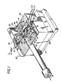
- FIGS. 1 and 2 A high frequency laser diode mount 10 formed in accordance with the present invention is illustrated in FIGS. 1 and 2.
- An exemplary laser 12 is illustrated in these figures as a double heterostructure junction laser including a p-contact surface 14 and an n-contact surface 16.
- contact regions/layers and “wirebonds”. These "contact regions/ layers” are defined as metal layers, which may comprise any suitable material well known in the art, for example, aluminum.
- the wirebonds may be formed with any conventional wirebonding material, where gold is commonly used for this purpose.
- laser 12 receives a high frequency input signal I H via a stripline input connection.
- This stripline input includes a first metal contact 18 and a second metal contact 20, separated by a dielectric material 22.
- dielectric material 22 may comprise the external package material, if this material exhibits the required insulating properties.
- first metal contact 18 will be referred to as an n-contact and second metal contact 20 will be referred to as a p-contact. It is obvious, however, that the polarities of these two connections could be reversed.
- n-contact 18 and p-contact 20 are connected to laser 12 via a stripline 24 included on the mounting surface with laser 12.
- Stripline 24 includes a p-contact surface layer 26, a dielectric layer 28 disposed over a portion of p-contact layer 26, and an n-contact layer 30 disposed over dielectric layer 28.
- p-contact 20 is wire bonded to p-contact surface layer 26 and n-contact 18 is wired bonded to n-contact layer 30.
- n-contact 20 is wire bonded to p-contact surface layer 26 and n-contact 18 is wired bonded to n-contact layer 30.
- Layer 32 comprises a resistive element which is sized to provide the necessary impedance matching between laser 12 and stripline 24, as explained in detail hereinafter.
- resistive element 32 may comprise a conventional film (thin or thick) resistor deposit used to provide a resistive element in integrated circuits.
- a thin film tantalum resistor may be used to form layer 32.
- Stripline 24 is connected to laser 12 through a laser mounting structure (also referred to as a submount) including an n-contact mounting layer 34 and p-contact surface layer 26, where n-contact mounting layer 34 is separated from p-contact surface layer 26 by a dielectric layer 36.
- N-side 16 of laser 12 is directly bonded (for example, indium bonded) to n-contact mounting layer 34 to complete the negative polarity electrical connection.
- P-side 14 of laser 12 is wire bonded to p-contact surface layer 26 to complete the positive polarity connection.
- mount 10 also provides for the connection of low frequency (less than 500 Mb/S) input signals to laser 12, where this input does not require using stripline 24 and is, in fact, electrically isolated from stripline 24.
- contact may be made directly to p-side 14 of laser 12 via a wire bond connection P2 extending to layer 26.
- Layer 26 is connected (FIG. 2) by a wire Lfp to an input signal source (not shown).
- An additional n-contact region 38 is included in mount 10, wherein region 38 is wired bonded to n-contact mounting layer 34.
- n-contact region 38 may be wire bonded by a connection denoted Lfn to the external signal source.
- a dc bias signal may be connected via wire bond Lfn to n-contact region 38, through n-contact mounting layer 34 and layer 36 to the power supply (not shown).
- FIG. 1 A feedback monitoring arrangement may be used.
- a PIN photodiode 40 is used as a monitoring element and is located behind laser 12 in the manner illustrated in FIG. 1. Since laser 12 will emit light in both directions, it is not necessary for the monitoring arrangement to be directly in the path of the output signal.
- a reflective groove 42 comprising an angle of, for example, 45°, is included in the portion of mount 10 holding PIN photodiode 40 so that the backface light from laser 12 may be redirected into the front major surface of n-layer 44 of PIN photodiode 40.
- PIN photodiode 40 Utilizing this reflective groove structure allows PIN photodiode 40 to be attached to mount 10 along a major surface area as shown, providing a much more rugged contact than if the major surface of n-layer 40 had to be positioned directly in the light beam path of the backface of laser 12.
- P-contact 46 of PIN photodiode 40 is wirebonded to a p-contact mount 48, for subsequent connection to an external monitor (not shown), where this external monitor, in response to the output signal from PIN photodiode 40, is used to control the operation of the input source.
- a temperature sensor 50 for example a thermistor
- mount 10 may include a thermo-electric cooler as an integral part of the mount.
- One such cooler 60 is illustrated as the base of mount 10.
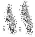
- n-contact 18 is connected to n-contact layer 30 by a wirebond denoted n1 (where as discussed above, a multiple wirebond would be used in practice).
- p-contact 20 is connected to p-contact surface layer 26 by a wirebond p1, p-contact surface layer 26 extends fully under the portion of the mount supporting laser 12.
- a dielectric layer 28 is positioned between contact layers 26 and 30, so as to form a three-level parallel-plate stripline structure.
- the characteristic impedance Z o of stripline 24 is a function of the thickness t , width w , and dielectric constant ⁇ of dielectric layer 28.
- the value for ⁇ is defined by the material and the necessary thickness t and width w are determined by standard methods well known in the art.
- resistor 32 is included in stripline 24 to control the resistance seen looking from the high frequency modulation current source into laser 12. The inclusion of resistor 32 not only serves to increase this internal resistance, but also provides a means of providing an impedance between the current source and laser 12 which is independent of the actual impedance of the laser used.
- a particular laser after a particular laser is mounted, its impedance can be measured and the required additional resistance added. For example, a given laser exhibits an impedance of 6.25 ohms. A resistor 32 of value Z-6.25 ohms may then be formed on stripline 24 to provide the desired value of Z ohms. Likewise, if a laser exhibited an internal resistance of 8 ohms, a resistor 3 of Z-8 ohms would be formed on stripline 32. This ability to control the input resistance is an important aspect of the present invention.
- stripline 4 is connected to laser 12 using a pair of (multiple) wirebonds.
- p-side 14 of laser 12 is connected by a wirebond p2 to p-contact surface layer 26.
- N-side 16 of laser 12 is directly soldered to n-contact mounting surface 34, where mounting surface 34 is connected by a wirebond n2 to n-contact layer 32.
- the alternative low-frequency connections are connected as shown FIG. 2, where a third wirebond n3 is used to connect n-contact mounting surface 34 to n-contact region 38. As stated above, this third connection allows for the dc bias potential to be connected through the various n-contact layers back to the high frequency signal source. As shown in FIG.
- n-contact mounting surface 34 is separated from p-contact surface layer 26 by a dielectric surface layer 36.
- Layer 36 functions not only to keep the p-contact away from the n-contact, but also allows the combination of layers 26, 34 and 36 to form another stripline, thus allowing the stripline transmission quality of the input signal to be passed directly to the laser.
- surface layer 36 comprises a material which is capable of absorbing the heat generated by laser 12 and passing this heat along to TEC 60. Beryllia is one such material that may be used to form layer 36.
- an additional p-contact mount 72 is included to raise the level of wirebond p2 to coincide with the level of p-side 14 of laser 12, where this level is indicated as d in FIG. 3.
- mount 72 may include a metal spacer element 74 (which may be aluminum) that is soldered directly to p-contact surface layer 26 to provide electrical connection.
- a top surface contact layer 76 is soldered to spacer 74 and wirebond p2 is attached between p-side 14 of laser 12 and elevated p-contact 76.
Landscapes
- Physics & Mathematics (AREA)
- Condensed Matter Physics & Semiconductors (AREA)
- General Physics & Mathematics (AREA)
- Electromagnetism (AREA)
- Optics & Photonics (AREA)
- Semiconductor Lasers (AREA)
Claims (8)
Applications Claiming Priority (2)
| Application Number | Priority Date | Filing Date | Title |
|---|---|---|---|
| US792055 | 1985-10-28 | ||
| US06/792,055 US4761788A (en) | 1985-10-28 | 1985-10-28 | Stripline mount for semiconductor lasers |
Publications (2)
| Publication Number | Publication Date |
|---|---|
| EP0252094A1 EP0252094A1 (de) | 1988-01-13 |
| EP0252094B1 true EP0252094B1 (de) | 1991-03-13 |
Family
ID=25155658
Family Applications (1)
| Application Number | Title | Priority Date | Filing Date |
|---|---|---|---|
| EP86907070A Expired - Lifetime EP0252094B1 (de) | 1985-10-28 | 1986-10-28 | Streifenleitungsaufbau für halbleiterlaser |
Country Status (5)
| Country | Link |
|---|---|
| US (1) | US4761788A (de) |
| EP (1) | EP0252094B1 (de) |
| JP (1) | JPS63501187A (de) |
| CA (1) | CA1254294A (de) |
| WO (1) | WO1987002834A1 (de) |
Families Citing this family (24)
| Publication number | Priority date | Publication date | Assignee | Title |
|---|---|---|---|---|
| JPH073907B2 (ja) * | 1987-07-03 | 1995-01-18 | 株式会社日立製作所 | デュアルインラインパッケ−ジ形半導体レ−ザモジュ−ル |
| JPH0817260B2 (ja) * | 1987-12-18 | 1996-02-21 | 株式会社日立製作所 | 駆動回路内蔵半導体レーザモジユール |
| JPH0714102B2 (ja) * | 1988-01-28 | 1995-02-15 | 三菱電機株式会社 | 光結合装置 |
| US4937660A (en) * | 1988-12-21 | 1990-06-26 | At&T Bell Laboratories | Silicon-based mounting structure for semiconductor optical devices |
| JP2654988B2 (ja) * | 1989-06-09 | 1997-09-17 | 松下電器産業株式会社 | 半導体レーザ装置 |
| NL8901523A (nl) * | 1989-06-16 | 1991-01-16 | Philips Nv | Laserdiode module. |
| US5264392A (en) * | 1990-07-05 | 1993-11-23 | At&T Bell Laboratories | Fabrication technique for silicon-based optical subassemblies |
| US5113404A (en) * | 1990-07-05 | 1992-05-12 | At&T Bell Laboratories | Silicon-based optical subassembly |
| DE4110378A1 (de) * | 1991-03-28 | 1992-10-01 | Standard Elektrik Lorenz Ag | Einrichtung mit einem traegerteil, einem halbleiterlaser und kontaktierungen |
| FR2696603B1 (fr) * | 1992-10-05 | 1995-01-06 | France Telecom | Tête laser perfectionnée. |
| US5444564A (en) * | 1994-02-09 | 1995-08-22 | Hughes Aircraft Company | Optoelectronic controlled RF matching circuit |
| JPH07288351A (ja) * | 1994-04-19 | 1995-10-31 | Fujitsu Ltd | ペルチェ制御回路及びその素子構造 |
| JP3553222B2 (ja) * | 1995-09-20 | 2004-08-11 | 三菱電機株式会社 | 光変調器モジュール |
| KR0171374B1 (ko) * | 1995-11-17 | 1999-05-01 | 양승택 | 광집속렌즈를 포함하는 레이저 모듈 및 그 렌즈 고정방법 |
| US5982793A (en) * | 1996-05-20 | 1999-11-09 | Matsushita Electric Industrial Co., Ltd. | Semiconductor laser module with internal matching circuit |
| EP0961372B1 (de) * | 1998-05-26 | 2002-07-10 | Infineon Technologies AG | Hochfrequenz-Lasermodul und Verfahren zur Herstellung desselben |
| US6320706B1 (en) | 2000-02-24 | 2001-11-20 | Lightwave Electronics | Method and apparatus for positioning and fixating an optical element |
| CN100428592C (zh) * | 2001-03-05 | 2008-10-22 | 富士施乐株式会社 | 发光元件驱动装置和发光元件驱动系统 |
| DE60101308T2 (de) | 2001-03-30 | 2004-08-26 | Agilent Technologies, Inc. (n.d.Ges.d.Staates Delaware), Palo Alto | Laserdiodenanpassungsschaltung und Impedanzanpassungsverfahren dafür |
| US7049759B2 (en) * | 2001-12-06 | 2006-05-23 | Linear Technology Corporation | Circuitry and methods for improving the performance of a light emitting element |
| EP1389812A1 (de) * | 2002-08-13 | 2004-02-18 | Agilent Technologies Inc | Montierungsanordnung für hochfrequente Elektrooptische Elemente |
| KR101473650B1 (ko) | 2012-11-30 | 2014-12-17 | (주) 빛과 전자 | 온도 조절이 가능한 고속 전송용 레이저 다이오드 |
| US9859680B2 (en) | 2013-12-17 | 2018-01-02 | Lasermax, Inc. | Shock resistant laser module |
| CN111969397B (zh) * | 2020-08-17 | 2023-10-24 | 索尔思光电股份有限公司 | 一种包边封装的tosa及光模块 |
Family Cites Families (11)
| Publication number | Priority date | Publication date | Assignee | Title |
|---|---|---|---|---|
| US3757259A (en) * | 1972-04-28 | 1973-09-04 | Us Army | Novel mounting technique for glass package diodes |
| US4023198A (en) * | 1974-08-16 | 1977-05-10 | Motorola, Inc. | High frequency, high power semiconductor package |
| JPS5137548A (en) * | 1974-09-26 | 1976-03-29 | Daiichi Denshi Kogyo | Dojikugatainpiidansuhenkanpatsudoyokaadoatsuteneeta narabini dojikugatainpiidansuhenkanpatsudo |
| GB1487010A (en) * | 1975-04-01 | 1977-09-28 | Standard Telephones Cables Ltd | Laser stud mounts |
| DE2737345C2 (de) * | 1976-08-20 | 1991-07-25 | Canon K.K., Tokio/Tokyo | Halbleiterlaser-Vorrichtung mit einem Peltier-Element |
| US4297653A (en) * | 1979-04-30 | 1981-10-27 | Xerox Corporation | Hybrid semiconductor laser/detectors |
| US4301429A (en) * | 1979-06-07 | 1981-11-17 | Raytheon Company | Microwave diode with high resistance layer |
| NL181963C (nl) * | 1979-06-26 | 1987-12-01 | Philips Nv | Halfgeleiderlaserinrichting. |
| JPS594145A (ja) * | 1982-06-30 | 1984-01-10 | Fujitsu Ltd | 半導体装置 |
| GB2124402B (en) * | 1982-07-27 | 1986-01-22 | Standard Telephones Cables Ltd | Injection laser packages |
| DE3330434A1 (de) * | 1983-08-19 | 1985-03-07 | Heinrich-Hertz-Institut für Nachrichtentechnik Berlin GmbH, 1000 Berlin | Stabilisationseinrichtung fuer einen halbleiter-laser |
-
1985
- 1985-10-28 US US06/792,055 patent/US4761788A/en not_active Expired - Lifetime
-
1986
- 1986-10-28 JP JP61506095A patent/JPS63501187A/ja active Granted
- 1986-10-28 WO PCT/US1986/002305 patent/WO1987002834A1/en not_active Ceased
- 1986-10-28 EP EP86907070A patent/EP0252094B1/de not_active Expired - Lifetime
- 1986-10-28 CA CA000521619A patent/CA1254294A/en not_active Expired
Non-Patent Citations (1)
| Title |
|---|
| Review of Scientific Instruments, vol. 52, no. 1, January 1981, P.R. Smith et al. "Thin film photoconductor mounting schemes for picosecond optical detectors", page 138-140 * |
Also Published As
| Publication number | Publication date |
|---|---|
| WO1987002834A1 (en) | 1987-05-07 |
| EP0252094A1 (de) | 1988-01-13 |
| CA1254294A (en) | 1989-05-16 |
| JPH0482196B2 (de) | 1992-12-25 |
| JPS63501187A (ja) | 1988-04-28 |
| US4761788A (en) | 1988-08-02 |
Similar Documents
| Publication | Publication Date | Title |
|---|---|---|
| EP0252094B1 (de) | Streifenleitungsaufbau für halbleiterlaser | |
| US7130100B2 (en) | Optical module | |
| US6940091B2 (en) | Semiconductor laser module and semiconductor laser apparatus | |
| JP2995209B2 (ja) | レーザダイオードモジュール | |
| JP4199901B2 (ja) | 光送信モジュール | |
| CN1617402A (zh) | 晶体管外形罐型光模块 | |
| EP0632550A2 (de) | Modulation von Laserdioden | |
| JP2004356233A (ja) | 半導体レーザモジュールおよび半導体レーザ装置 | |
| JPWO2021014568A1 (ja) | To−can型光送信モジュール | |
| CN1512209A (zh) | 高速的基于to-can的光模块 | |
| US4937660A (en) | Silicon-based mounting structure for semiconductor optical devices | |
| US7034641B1 (en) | Substrate structure for photonic assemblies and the like having a low-thermal-conductivity dielectric layer on a high-thermal-conductivity substrate body | |
| JP7020590B1 (ja) | レーザ光源装置 | |
| US6810049B2 (en) | Semiconductor laser device and semiconductor laser module | |
| JP4090401B2 (ja) | 光送信モジュール | |
| JPS63501185A (ja) | 多層セラミックレ−ザパッケ−ジ | |
| JP2000353846A (ja) | ステム型半導体レーザ装置 | |
| WO2024134864A1 (ja) | 光モジュール | |
| JP2500591B2 (ja) | 半導体レ―ザ装置 | |
| JP7635886B2 (ja) | 半導体レーザ光源装置 | |
| US5812715A (en) | Optoelectronic device with a coupling between a semiconductor diode laser modulator or amplifier and two optical glass fibers | |
| JP3460222B2 (ja) | 半導体レーザモジュール | |
| US20240222929A1 (en) | Optical communication device | |
| JPH05110201A (ja) | 半導体レーザ装置 | |
| JPH02197185A (ja) | 電子式冷却素子内蔵半導体レーザアセンブリ |
Legal Events
| Date | Code | Title | Description |
|---|---|---|---|
| PUAI | Public reference made under article 153(3) epc to a published international application that has entered the european phase |
Free format text: ORIGINAL CODE: 0009012 |
|
| 17P | Request for examination filed |
Effective date: 19871007 |
|
| AK | Designated contracting states |
Kind code of ref document: A1 Designated state(s): DE FR GB NL SE |
|
| 17Q | First examination report despatched |
Effective date: 19891027 |
|
| GRAA | (expected) grant |
Free format text: ORIGINAL CODE: 0009210 |
|
| AK | Designated contracting states |
Kind code of ref document: B1 Designated state(s): DE FR GB NL SE |
|
| PG25 | Lapsed in a contracting state [announced via postgrant information from national office to epo] |
Ref country code: SE Effective date: 19910313 Ref country code: NL Effective date: 19910313 |
|
| REF | Corresponds to: |
Ref document number: 3678165 Country of ref document: DE Date of ref document: 19910418 |
|
| ET | Fr: translation filed | ||
| NLV1 | Nl: lapsed or annulled due to failure to fulfill the requirements of art. 29p and 29m of the patents act | ||
| PLBE | No opposition filed within time limit |
Free format text: ORIGINAL CODE: 0009261 |
|
| STAA | Information on the status of an ep patent application or granted ep patent |
Free format text: STATUS: NO OPPOSITION FILED WITHIN TIME LIMIT |
|
| 26N | No opposition filed | ||
| PGFP | Annual fee paid to national office [announced via postgrant information from national office to epo] |
Ref country code: FR Payment date: 20010925 Year of fee payment: 16 |
|
| PGFP | Annual fee paid to national office [announced via postgrant information from national office to epo] |
Ref country code: GB Payment date: 20011008 Year of fee payment: 16 |
|
| PGFP | Annual fee paid to national office [announced via postgrant information from national office to epo] |
Ref country code: DE Payment date: 20011230 Year of fee payment: 16 |
|
| REG | Reference to a national code |
Ref country code: GB Ref legal event code: IF02 |
|
| PG25 | Lapsed in a contracting state [announced via postgrant information from national office to epo] |
Ref country code: GB Free format text: LAPSE BECAUSE OF NON-PAYMENT OF DUE FEES Effective date: 20021028 |
|
| PG25 | Lapsed in a contracting state [announced via postgrant information from national office to epo] |
Ref country code: DE Free format text: LAPSE BECAUSE OF NON-PAYMENT OF DUE FEES Effective date: 20030501 |
|
| GBPC | Gb: european patent ceased through non-payment of renewal fee | ||
| PG25 | Lapsed in a contracting state [announced via postgrant information from national office to epo] |
Ref country code: FR Free format text: LAPSE BECAUSE OF NON-PAYMENT OF DUE FEES Effective date: 20030630 |
|
| REG | Reference to a national code |
Ref country code: FR Ref legal event code: ST |