EP0247699A1 - Bildaufzeichnungsträger für einen elektrostatischen Drucker und Drucker, in dem ein Träger dieser Art benutzt wird - Google Patents
Bildaufzeichnungsträger für einen elektrostatischen Drucker und Drucker, in dem ein Träger dieser Art benutzt wird Download PDFInfo
- Publication number
- EP0247699A1 EP0247699A1 EP87201008A EP87201008A EP0247699A1 EP 0247699 A1 EP0247699 A1 EP 0247699A1 EP 87201008 A EP87201008 A EP 87201008A EP 87201008 A EP87201008 A EP 87201008A EP 0247699 A1 EP0247699 A1 EP 0247699A1
- Authority
- EP
- European Patent Office
- Prior art keywords
- electrodes
- image
- forming element
- support
- forming
- Prior art date
- Legal status (The legal status is an assumption and is not a legal conclusion. Google has not performed a legal analysis and makes no representation as to the accuracy of the status listed.)
- Granted
Links
- 239000010410 layer Substances 0.000 claims abstract description 34
- 230000002093 peripheral effect Effects 0.000 claims abstract description 5
- 239000002344 surface layer Substances 0.000 claims abstract description 5
- 238000007639 printing Methods 0.000 claims abstract description 4
- 230000005291 magnetic effect Effects 0.000 claims description 15
- 239000000843 powder Substances 0.000 claims description 13
- 230000005684 electric field Effects 0.000 claims 1
- 239000002184 metal Substances 0.000 description 7
- 229910052751 metal Inorganic materials 0.000 description 7
- 238000000034 method Methods 0.000 description 7
- 239000000463 material Substances 0.000 description 6
- 239000002966 varnish Substances 0.000 description 4
- 229910052729 chemical element Inorganic materials 0.000 description 2
- 239000000306 component Substances 0.000 description 2
- 238000010438 heat treatment Methods 0.000 description 2
- 230000003287 optical effect Effects 0.000 description 2
- 239000004593 Epoxy Substances 0.000 description 1
- 230000015572 biosynthetic process Effects 0.000 description 1
- 230000015556 catabolic process Effects 0.000 description 1
- 239000011248 coating agent Substances 0.000 description 1
- 238000000576 coating method Methods 0.000 description 1
- 239000004020 conductor Substances 0.000 description 1
- 238000010276 construction Methods 0.000 description 1
- 230000001419 dependent effect Effects 0.000 description 1
- 239000003989 dielectric material Substances 0.000 description 1
- 238000009713 electroplating Methods 0.000 description 1
- 238000005516 engineering process Methods 0.000 description 1
- 239000003822 epoxy resin Substances 0.000 description 1
- 239000011810 insulating material Substances 0.000 description 1
- 238000012423 maintenance Methods 0.000 description 1
- 238000004377 microelectronic Methods 0.000 description 1
- 229920000647 polyepoxide Polymers 0.000 description 1
- 239000002904 solvent Substances 0.000 description 1
Images
Classifications
-
- B—PERFORMING OPERATIONS; TRANSPORTING
- B41—PRINTING; LINING MACHINES; TYPEWRITERS; STAMPS
- B41C—PROCESSES FOR THE MANUFACTURE OR REPRODUCTION OF PRINTING SURFACES
- B41C1/00—Forme preparation
-
- G—PHYSICS
- G03—PHOTOGRAPHY; CINEMATOGRAPHY; ANALOGOUS TECHNIQUES USING WAVES OTHER THAN OPTICAL WAVES; ELECTROGRAPHY; HOLOGRAPHY
- G03G—ELECTROGRAPHY; ELECTROPHOTOGRAPHY; MAGNETOGRAPHY
- G03G15/00—Apparatus for electrographic processes using a charge pattern
- G03G15/22—Apparatus for electrographic processes using a charge pattern involving the combination of more than one step according to groups G03G13/02 - G03G13/20
- G03G15/34—Apparatus for electrographic processes using a charge pattern involving the combination of more than one step according to groups G03G13/02 - G03G13/20 in which the powder image is formed directly on the recording material, e.g. by using a liquid toner
- G03G15/344—Apparatus for electrographic processes using a charge pattern involving the combination of more than one step according to groups G03G13/02 - G03G13/20 in which the powder image is formed directly on the recording material, e.g. by using a liquid toner by selectively transferring the powder to the recording medium, e.g. by using a LED array
- G03G15/348—Apparatus for electrographic processes using a charge pattern involving the combination of more than one step according to groups G03G13/02 - G03G13/20 in which the powder image is formed directly on the recording material, e.g. by using a liquid toner by selectively transferring the powder to the recording medium, e.g. by using a LED array using a stylus or a multi-styli array
-
- G—PHYSICS
- G03—PHOTOGRAPHY; CINEMATOGRAPHY; ANALOGOUS TECHNIQUES USING WAVES OTHER THAN OPTICAL WAVES; ELECTROGRAPHY; HOLOGRAPHY
- G03G—ELECTROGRAPHY; ELECTROPHOTOGRAPHY; MAGNETOGRAPHY
- G03G2217/00—Details of electrographic processes using patterns other than charge patterns
- G03G2217/0075—Process using an image-carrying member having an electrode array on its surface
Definitions
- This invention relates to an image-forming element for an electrostatic printer, consisting of an endless support with a dielectric surface layer thereon.
- US Patent 3 816 840 describes an electrostatic printing process and printer in which a dielectric image-receiving material is fed between a first and a second electrode which are disposed a short distance apart and one of which is covered with a layer of magnetically attractable electrically conductive toner powder, while voltage pulses are applied between the said electrodes so that toner powder is deposited on the image-receiving material in the form of an information pattern.
- a disadvantage of this process is that only dielectric image-receiving material can be used, thus restricting the choice of image-receiving materials.
- US Patent 3 946 402 describes an electrostatic printer comprising a rotatable drum provided with a dielectric layer on which a uniform layer of electrically conductive magnetically attractable toner powder is applied.
- a magnetic roller is disposed in an image-forming zone near the drum surface covered with toner powder and has a stationary non-magnetic sleeve and a rotatable magnet system mounted inside the sleeve.
- a large number of magnetic electrodes in the form of rods each connected to a voltage supply is disposed axially on the sleeve of this magnetic roller.
- the electrodes are conductive they must be insulated from one another.
- a disadvantage of this known device is that the conductive toner powder can short-circuit some electrodes, thus disturbing the image formation. It is also a very complex and expensive matter to construct a row of fine magnetic electrodes in rod form.
- an image-forming element for an electrostatic printer is provided with which the above disadvantages can be obviated.
- this object is attained by providing an image-forming element of the kind referred to in the preamble, characterised in that image-forming electrodes are provided beneath the dielectric surface layer, said electrodes being insultated from one another and extending in the form of endless paths parallel to one another in the peripheral direction of the support and in that electrodes are provided beneath the said electrodes and are also insulated from one another and extend each from a point near one end of the support in the direction of the other end of the support, one in each case of said latter electrodes being electrically conductive connected to one in each case of the electrodes extending in the peripheral direction, and said latter electrodes being also connected to means for supplying voltage to said electrodes.
- the electrodes are completely insulated from one another so that short-circuiting of one or more electrodes by the applied electrically conductive toner is obviated. Since the image-forming electrodes are disposed in the image-forming element itself, a conventional magnetic roller can be used in the image forming process. This results in a simpler and cheaper construction apart from better copy quality.
- the electronic facilities for energising the electrodes in accordance with an information pattern requiring to be printed are disposed near one or both ends of the support on the periphery thereof.
- the invention also provides a device for printing information using an image-forming element according to the invention.
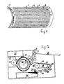
- the image-forming element according to Fig. 1 comprises a drum 1 having an insulating surface on which a plurality of electrodes 2 are disposed, which extend axially to the drum 1.
- Each electrode 2 is connected to one of the blocks 3 which are disposed on one side of the drum 1 and which contain the electronic facilities for selectively applying voltage to the electrodes 2 in accordance with an information pattern.
- the electrodes 2 are covered with an insulating layer which, however, has been omitted from Fig. 1 for the sake of clarity.
- Electrodes 4 are disposed on this insulating layer and extend in the direction of the periphery of the drum 1 in the form of endless paths parallel to one another equidistantly.
- One electrode 4 in each case is conductively connected to one electrode 2 in each case via perforations in the intermediate insulating layer, such perforations being filled with conductive material.
- the conductive connections are indicated in the form of dots 5 in Fig. 1. That part of the drum 1 which is covered with the electrodes 4 is covered with a dielectric layer which again has been omitted in Fig. 1. Thus apart from the conductive connections 5 the electrodes 2 and 4 are completely insulated from one another.
- the number of electrodes 2 on the drum 1 is equal to the number of electrodes 4, one electrode 2 in each case being conductively connected to one electrode 4 in each case.
- the quality of the images formed on the image-forming element depends, inter alia on the number of electrodes 4. As the electrode density increases so the image quality improves.
- the number of electrodes 4 is at least ten per millimetre, and preferably fourteen to twenty per millimetre. According to a preferred embodiment, the number of electrodes 4 is equal to sixteen per millimetre, the electrodes 4 having a width of about 40 micrometers and the distance between the electrodes being about 20 micrometers.
- the electronic control blocks 3 each comprise a plurality of integrated circuits known, for example, from video display tech niques, comprising a serial-in parallel-out shift register, an output register and connected thereto drivers with a voltage range of 15 to 25 volts for example.
- Each electrode 2 is connected to a driver of one of the integrated circuits provided.
- the image-forming element according to the invention can be made by applying an electrically conductive metal layer, e.g. copper, to a drum having an insulating surface, or having a conductive surface provided with an insulating layer, in known manner, e.g. by vapour-coating or electroplating, and then converting this metal layer to a pattern of electrodes 2 extending transversely, e.g. by the use of a known photo-etch technique. That part of the drum surface, on which the peripherally extending electrodes 4 should be disposed is then covered with an insulating layer and perforations are formed in this insulating layer, e.g.
- an electrically conductive metal layer e.g. copper
- the perforations may alternatively be formed photographically by covering the drum surface provided with the electrodes 2 with a light-sensitive layer of varnish, exposing this layer of varnish to light except for the places where the perforations 5 are to be formed, and removing the unexposed parts of the layer of varnish by means of a suitable solvent. The exposed layer of varnish then acts as an insulating intermediate layer. After the perforations have been formed in the insulating layer, a conductive metal layer is applied over this insulating layer, the perforations being filled at the same time.
- This metal layer can be applied in the same way and can consist of the same material as the metal layer from which the electrodes 2 were formed.
- the peripherally extending electrodes 4 are then formed from this metal layer, e.g. again by using a known photo-etch technique, each electrode 4 of course being formed where an electrical connection is achieved between the metal layer and one of the electrodes 2 situated there-beneath.
- that part of the drum 1 provided with the electrodes 4 is covered with a smooth dielectric layer so that the electrodes 4 are completely insulated from one another.
- the electronic blocks 3 for selectively controlling the electrodes 2 are then secured to the side of the drum by fixing techniques known per se.
- the insulating layer which separates the electrodes 2 from the electrodes 4 is, for example, of a thickness of at least 5 micrometers and has a breakdown voltage of, for example, of 100 V or more.
- the layer can be formed by means of known insulating materials.
- a suitable material for forming this insulating layer is epoxy resin, e.g. Epo-tek type 360 or 353 ND made by Messrs. Epoxy Technology Inc.
- the dielectric top layer applied over the electrodes 4 preferably has a thickness of just a few tenths of a micrometer, (e.g. 0.2 to 0.8 micrometers). Suitable dielectric materials for forming this layer are known, inter alia , from microelectronics.
- the electronic blocks 3 for controlling the electrodes 2 are disposed along one side of the drum. It will be apparent that these blocks can be distributed also over both sides of the drum 1.
- the fact that the electronic components are disposed on the outer surface of the drum 1 has the advantage that they are readily accessible and can therefore readily be replaced in the event of a fault. It is also possible to dispose the electronics for controlling the electrodes 2 inside the drum 1 and to connect the electrodes 2 to the electronics via the sides of the drum by separate connecting leads.
- the electrodes 2 extending transversely to the drum 1 need not extend axially nor need they cover all the complete working width of the drum 1. Of course they need only extend to the place where the electrically conductive connection is established with the electrode 4 thereabove.
- Fig. 2 diagrammatically illustrates a printer equipped with an image-forming element according to the invention, which element has the reference 10 in this Figure.
- a magnetic roller 12 is disposed a short distance from the surface of the image-forming element 10 and comprises a rotatable electrically conductive non-magnetic sleeve and an internal stationary magnet system.
- the rotatable sleeve of the magnetic roller 12 is convered with a uniform layer of electrically conductive and magnetically attractable toner powder which in an image-forming zone 13 is in contact with the image-forming element 10.
- a powder image is formed on the image-forming element 10.
- This powder image is transferred by pressure to a heated rubber-covered roller 14.
- a sheet of paper is taken by roller 25 and fed via guideways 24 and rollers 22 and 23 to a heating station 19.
- the heating station 19 comprises a belt 21 trained about a heated roller 20.
- the sheet of paper is heated by contact with the belt 21.
- the sheet heated in this way is then fed through rollers 14 and 15, the softened image present on roller 14 being completely transferred to the sheet of paper.
- the temperatures of the belt 21 and the roller 14 are so adjusted to one another that the image fuses on the sheet of paper.
- Unit 30 comprises an electronic circuit which converts the optical information of an original into electrical signals which are fed, via leads 31 having slide contacts, and conductive tracks 32 in the insulating side wall of image-forming element 10, to the electronic blocks 3 connected to the tracks 32.
- the information is fed serially line by line to the shift register of the integrated circuits on the blocks 3. If the shift registers are completely filled in accordance with the information of one line, that information is put into the output register and via the drivers the electrodes 2, 4 are actuated or not dependent on the signal. While this line is being printed the information of the next line is being fed to the shift registers.
- electrical signals originating from a computer or a data processing device can also be converted in unit 30 to signals which are fed to the electronic blocks 3.
- the electrically conductive magnetically attractable toner powder is fed to the image-forming zone 13 by the magnetic roller 12. It will also be clear that the toner powder can also be applied in a uniform layer to the image-forming element 10 and then be selectively removed therefrom in the image-forming zone 13 as described in the above-mentioned US Patent 3 946 402. Other variants of the invention will be apparent to the skilled addressee but they all come under the invention as described in the following claims.
Landscapes
- Physics & Mathematics (AREA)
- General Physics & Mathematics (AREA)
- Engineering & Computer Science (AREA)
- Manufacturing & Machinery (AREA)
- Printers Or Recording Devices Using Electromagnetic And Radiation Means (AREA)
- Electrophotography Using Other Than Carlson'S Method (AREA)
- Dot-Matrix Printers And Others (AREA)
Applications Claiming Priority (2)
| Application Number | Priority Date | Filing Date | Title |
|---|---|---|---|
| NL8601376 | 1986-05-29 | ||
| NL8601376A NL8601376A (nl) | 1986-05-29 | 1986-05-29 | Beeldvormingselement voor een elektrostatische drukinrichting, alsmede een drukinrichting waarin zulk een element wordt toegepast. |
Publications (2)
| Publication Number | Publication Date |
|---|---|
| EP0247699A1 true EP0247699A1 (de) | 1987-12-02 |
| EP0247699B1 EP0247699B1 (de) | 1991-08-14 |
Family
ID=19848087
Family Applications (1)
| Application Number | Title | Priority Date | Filing Date |
|---|---|---|---|
| EP87201008A Expired EP0247699B1 (de) | 1986-05-29 | 1987-05-29 | Bildaufzeichnungsträger für einen elektrostatischen Drucker und Drucker, in dem ein Träger dieser Art benutzt wird |
Country Status (5)
| Country | Link |
|---|---|
| US (1) | US4748464A (de) |
| EP (1) | EP0247699B1 (de) |
| JP (1) | JP2568848B2 (de) |
| DE (1) | DE3772103D1 (de) |
| NL (1) | NL8601376A (de) |
Cited By (10)
| Publication number | Priority date | Publication date | Assignee | Title |
|---|---|---|---|---|
| EP0595388A1 (de) * | 1992-10-30 | 1994-05-04 | Océ-Nederland B.V. | Bilderzeugerherstellungsverfahren und ein Datenwiedergabedruckgerät |
| EP0635768A1 (de) * | 1993-07-23 | 1995-01-25 | Océ-Nederland B.V. | Bilderzeugungsvorrichtung und Bilderzeugungselement zur Verwendung in dieser Vorrichtung |
| EP0718721A1 (de) | 1994-12-23 | 1996-06-26 | Océ-Nederland B.V. | Verfahren zur Aufnahme von Bildern und Bildaufnahmegerät zur Anwendung dieses Verfahrens |
| EP0803783A1 (de) * | 1996-04-25 | 1997-10-29 | Océ-Technologies B.V. | Bildaufzeichnungsträger und Verfahren zu seiner Herstellung |
| EP0803782A1 (de) * | 1996-04-25 | 1997-10-29 | Océ-Technologies B.V. | Verfahren zur Herstellung eines Bildaufzeichnungselement |
| US5742320A (en) * | 1993-12-08 | 1998-04-21 | Oce-Technologies, B.V. | Image-forming device and an image-forming element for use therein |
| US6014157A (en) * | 1996-04-25 | 2000-01-11 | Oce-Technologies B.V. | Image forming element having accurate connection with the electronic components of the control unit |
| US6045679A (en) * | 1996-04-25 | 2000-04-04 | Oce-Technologies B.V. | Method for manufacturing an image-forming element |
| WO2002049849A1 (en) * | 2000-12-21 | 2002-06-27 | Array Ab | Direct printing apparatus and method |
| EP1980919A2 (de) | 2007-04-13 | 2008-10-15 | Samsung Electronics Co., Ltd | Bilderzeugungselement und Herstellungsverfahren dafür sowie Bilderzeugungsvorrichtung mit dem Bilderzeugungselement |
Families Citing this family (22)
| Publication number | Priority date | Publication date | Assignee | Title |
|---|---|---|---|---|
| JPH0293473A (ja) * | 1988-09-29 | 1990-04-04 | Toppan Printing Co Ltd | 電子印刷版及び電子印刷方法 |
| DE3836931C2 (de) * | 1988-10-29 | 1993-11-04 | Roland Man Druckmasch | Druckform fuer eine druckmaschine mit wiederholt aktivierbaren und loeschbaren bereichen |
| US6043830A (en) * | 1991-05-08 | 2000-03-28 | Cubital, Ltd. | Apparatus for pattern generation on a dielectric substrate |
| US5157423A (en) * | 1991-05-08 | 1992-10-20 | Cubital Ltd. | Apparatus for pattern generation on a dielectric substrate |
| US5508727A (en) * | 1991-05-08 | 1996-04-16 | Imagine, Ltd. | Apparatus and method for pattern generation on a dielectric substrate |
| DE69221255T2 (de) * | 1991-05-08 | 1998-03-12 | Cubital America Inc | Datenübertragungsvorrichtung |
| US5777576A (en) * | 1991-05-08 | 1998-07-07 | Imagine Ltd. | Apparatus and methods for non impact imaging and digital printing |
| US5927206A (en) * | 1997-12-22 | 1999-07-27 | Eastman Kodak Company | Ferroelectric imaging member and methods of use |
| US6100909A (en) * | 1998-03-02 | 2000-08-08 | Xerox Corporation | Matrix addressable array for digital xerography |
| US6184911B1 (en) * | 1998-06-03 | 2001-02-06 | Thomas N. Tombs | Apparatus and method for recording using an electrographic writer and an imaging web |
| JP4138106B2 (ja) * | 1998-10-22 | 2008-08-20 | セイコーエプソン株式会社 | 電子ペーパー用プリンター |
| JP3826013B2 (ja) * | 2001-02-28 | 2006-09-27 | キヤノン株式会社 | 画像形成装置 |
| US7121209B2 (en) * | 2004-01-16 | 2006-10-17 | Nandakumar Vaidyanathan | Digital semiconductor based printing system and method |
| WO2006113444A2 (en) * | 2005-04-13 | 2006-10-26 | Nandakumar Vaidyanathan | Digital semiconductor based printing system and method |
| WO2006113453A2 (en) * | 2005-04-13 | 2006-10-26 | Nandakumar Vaidyanathan | Digital semiconductor based printing system and method |
| JP2007008160A (ja) * | 2005-06-27 | 2007-01-18 | Oce Technologies Bv | 画像形成素子 |
| KR100653201B1 (ko) | 2005-11-30 | 2006-12-05 | 삼성전자주식회사 | 이미지 드럼 및 이미지 드럼의 제조방법 |
| DE102006013637A1 (de) * | 2006-03-22 | 2007-10-04 | Man Roland Druckmaschinen Ag | Druckform sowie Druckwerk einer Druckmaschine |
| KR100850716B1 (ko) * | 2006-12-01 | 2008-08-06 | 삼성전자주식회사 | 이미지형성체 및 그 제조방법 |
| KR20080112009A (ko) * | 2007-06-20 | 2008-12-24 | 삼성전자주식회사 | 화상형성장치 및 방법 |
| JP5569277B2 (ja) * | 2010-09-09 | 2014-08-13 | 富士ゼロックス株式会社 | 像保持体及びこれを用いた画像形成装置 |
| JP6502724B2 (ja) * | 2015-03-31 | 2019-04-17 | 株式会社Screenホールディングス | マグネットドラム、画像記録装置、および、マグネットドラムの製造方法 |
Citations (2)
| Publication number | Priority date | Publication date | Assignee | Title |
|---|---|---|---|---|
| US3739087A (en) * | 1970-10-26 | 1973-06-12 | Commw Of Australia | Multi point distributor head for signal recording or the like |
| GB2050948A (en) * | 1979-05-14 | 1981-01-14 | Jaouannet A | Writing head for an electrostatic point printer |
Family Cites Families (3)
| Publication number | Priority date | Publication date | Assignee | Title |
|---|---|---|---|---|
| US4397085A (en) * | 1980-12-05 | 1983-08-09 | International Business Machines Corporation | Method of manufacture of a multi-wire nonimpact printhead |
| JPS59150760A (ja) * | 1983-02-18 | 1984-08-29 | Fuji Xerox Co Ltd | 静電記録ヘツドの製造方法および装置 |
| JPS59230765A (ja) * | 1983-06-03 | 1984-12-25 | ダイナミクス・リサ−チ・コ−ポレ−シヨン | 静電プリントヘツド及びその製造方法 |
-
1986
- 1986-05-29 NL NL8601376A patent/NL8601376A/nl not_active Application Discontinuation
-
1987
- 1987-04-29 US US07/043,877 patent/US4748464A/en not_active Expired - Lifetime
- 1987-05-28 JP JP62133260A patent/JP2568848B2/ja not_active Expired - Fee Related
- 1987-05-29 EP EP87201008A patent/EP0247699B1/de not_active Expired
- 1987-05-29 DE DE8787201008T patent/DE3772103D1/de not_active Expired - Lifetime
Patent Citations (2)
| Publication number | Priority date | Publication date | Assignee | Title |
|---|---|---|---|---|
| US3739087A (en) * | 1970-10-26 | 1973-06-12 | Commw Of Australia | Multi point distributor head for signal recording or the like |
| GB2050948A (en) * | 1979-05-14 | 1981-01-14 | Jaouannet A | Writing head for an electrostatic point printer |
Non-Patent Citations (2)
| Title |
|---|
| PATENT ABSTRACTS OF JAPAN, vol. 9, no. 100 (M-376)[1823], 2nd May 1985; & JP-A-59 224 368 (FUJI XEROX K.K.) 17-12-1984 * |
| PATENT ABSTRACTS OF JAPAN, vol. 9, no. 100 (M-376)[1823], 2nd May 1985; & JP-A-59 224 369 (FUJI XEROX K.K.) 17-12-1984 * |
Cited By (14)
| Publication number | Priority date | Publication date | Assignee | Title |
|---|---|---|---|---|
| US5483269A (en) * | 1992-10-30 | 1996-01-09 | Oce - Nederland, B.V. | Process for the preparation of an image forming element and related printing device |
| EP0595388A1 (de) * | 1992-10-30 | 1994-05-04 | Océ-Nederland B.V. | Bilderzeugerherstellungsverfahren und ein Datenwiedergabedruckgerät |
| US5852455A (en) * | 1993-07-23 | 1998-12-22 | Oce-Nederland, B.V. | Image forming device, having separately energizable, inter-connected electrodes and image recording element for use, therein |
| EP0635768A1 (de) * | 1993-07-23 | 1995-01-25 | Océ-Nederland B.V. | Bilderzeugungsvorrichtung und Bilderzeugungselement zur Verwendung in dieser Vorrichtung |
| NL9301300A (nl) * | 1993-07-23 | 1995-02-16 | Oce Nederland Bv | Beeldvormingsinrichting, alsmede een beeldregistratie-element voor toepassing daarin. |
| US5742320A (en) * | 1993-12-08 | 1998-04-21 | Oce-Technologies, B.V. | Image-forming device and an image-forming element for use therein |
| EP0718721A1 (de) | 1994-12-23 | 1996-06-26 | Océ-Nederland B.V. | Verfahren zur Aufnahme von Bildern und Bildaufnahmegerät zur Anwendung dieses Verfahrens |
| US6040847A (en) * | 1994-12-23 | 2000-03-21 | Oce-Nederland B.V. | Method of recording images and an image-forming device for application of the method |
| EP0803782A1 (de) * | 1996-04-25 | 1997-10-29 | Océ-Technologies B.V. | Verfahren zur Herstellung eines Bildaufzeichnungselement |
| US6014157A (en) * | 1996-04-25 | 2000-01-11 | Oce-Technologies B.V. | Image forming element having accurate connection with the electronic components of the control unit |
| EP0803783A1 (de) * | 1996-04-25 | 1997-10-29 | Océ-Technologies B.V. | Bildaufzeichnungsträger und Verfahren zu seiner Herstellung |
| US6045679A (en) * | 1996-04-25 | 2000-04-04 | Oce-Technologies B.V. | Method for manufacturing an image-forming element |
| WO2002049849A1 (en) * | 2000-12-21 | 2002-06-27 | Array Ab | Direct printing apparatus and method |
| EP1980919A2 (de) | 2007-04-13 | 2008-10-15 | Samsung Electronics Co., Ltd | Bilderzeugungselement und Herstellungsverfahren dafür sowie Bilderzeugungsvorrichtung mit dem Bilderzeugungselement |
Also Published As
| Publication number | Publication date |
|---|---|
| JP2568848B2 (ja) | 1997-01-08 |
| JPS62292450A (ja) | 1987-12-19 |
| US4748464A (en) | 1988-05-31 |
| NL8601376A (nl) | 1987-12-16 |
| EP0247699B1 (de) | 1991-08-14 |
| DE3772103D1 (de) | 1991-09-19 |
Similar Documents
| Publication | Publication Date | Title |
|---|---|---|
| EP0247699B1 (de) | Bildaufzeichnungsträger für einen elektrostatischen Drucker und Drucker, in dem ein Träger dieser Art benutzt wird | |
| US4571602A (en) | Recording apparatus | |
| EP0000789B1 (de) | Verfahren und Vorrichtung zur Erzeugung geladener Teilchen | |
| JP2719615B2 (ja) | 画像形成要素の製造方法及び情報再生用印刷装置 | |
| US4704621A (en) | Printing device | |
| WO1994026527A1 (en) | Method for non-impact printing utilizing a multiplexed matrix of controlled electrode units and device to perform method | |
| US4733256A (en) | Electrostatic color printer | |
| US4777500A (en) | Electrostatic color printer | |
| US5889544A (en) | Electrographic printer with multiple transfer electrodes | |
| US5257046A (en) | Direct electrostatic printing with latent image assist | |
| EP0247694A1 (de) | Bildaufzeichnungsträger für einen elektrostatischen Drucker und Drucker, in dem ein Träger dieser Art benutzt wird | |
| EP0712055B1 (de) | Bilderzeugungsgerät | |
| JPH04304475A (ja) | 2レベル静電画像の選択的カラー化装置 | |
| US4837591A (en) | Highlight color imaging by depositing positive and negative ions on a substrate | |
| EP0635768B1 (de) | Bilderzeugungsvorrichtung und Bilderzeugungselement zur Verwendung in dieser Vorrichtung | |
| US5340617A (en) | Electrostatic patterning of multi-layer module lamina | |
| US3766850A (en) | Developing means for electrostatic printing apparatus | |
| US4038916A (en) | Electrostatic imaging apparatus | |
| EP0029641A1 (de) | Druckgerät | |
| EP0661611A2 (de) | Bilderzeugungsvorrichtung und Bilderzeugungselement zur Verwendung in dieser Vorrichtung | |
| US20060290765A1 (en) | Image-forming element | |
| WO1996006740A1 (en) | Electrostatic printhead utilizing multiplexed control electrodes and integrated drive circuits | |
| EP0991259A1 (de) | Bilderzeugungsgerät mit individuell-aktivierbaren Bilderzeugungselementen | |
| EP1739500A1 (de) | Bilderzeugungselement mit mehreren umkreisenden Elektroden | |
| JP2000326546A (ja) | 静電記録装置 |
Legal Events
| Date | Code | Title | Description |
|---|---|---|---|
| PUAI | Public reference made under article 153(3) epc to a published international application that has entered the european phase |
Free format text: ORIGINAL CODE: 0009012 |
|
| AK | Designated contracting states |
Kind code of ref document: A1 Designated state(s): DE FR GB NL |
|
| 17P | Request for examination filed |
Effective date: 19880511 |
|
| 17Q | First examination report despatched |
Effective date: 19900216 |
|
| GRAA | (expected) grant |
Free format text: ORIGINAL CODE: 0009210 |
|
| AK | Designated contracting states |
Kind code of ref document: B1 Designated state(s): DE FR GB NL |
|
| REF | Corresponds to: |
Ref document number: 3772103 Country of ref document: DE Date of ref document: 19910919 |
|
| ET | Fr: translation filed | ||
| PLBE | No opposition filed within time limit |
Free format text: ORIGINAL CODE: 0009261 |
|
| STAA | Information on the status of an ep patent application or granted ep patent |
Free format text: STATUS: NO OPPOSITION FILED WITHIN TIME LIMIT |
|
| 26N | No opposition filed | ||
| NLT1 | Nl: modifications of names registered in virtue of documents presented to the patent office pursuant to art. 16 a, paragraph 1 |
Owner name: OCE-TECHNOLOGIES B.V. |
|
| REG | Reference to a national code |
Ref country code: GB Ref legal event code: IF02 |
|
| PGFP | Annual fee paid to national office [announced via postgrant information from national office to epo] |
Ref country code: FR Payment date: 20040408 Year of fee payment: 18 |
|
| PGFP | Annual fee paid to national office [announced via postgrant information from national office to epo] |
Ref country code: GB Payment date: 20040415 Year of fee payment: 18 |
|
| PGFP | Annual fee paid to national office [announced via postgrant information from national office to epo] |
Ref country code: DE Payment date: 20040422 Year of fee payment: 18 |
|
| PGFP | Annual fee paid to national office [announced via postgrant information from national office to epo] |
Ref country code: NL Payment date: 20040518 Year of fee payment: 18 |
|
| PG25 | Lapsed in a contracting state [announced via postgrant information from national office to epo] |
Ref country code: GB Free format text: LAPSE BECAUSE OF NON-PAYMENT OF DUE FEES Effective date: 20050529 |
|
| PG25 | Lapsed in a contracting state [announced via postgrant information from national office to epo] |
Ref country code: NL Free format text: LAPSE BECAUSE OF NON-PAYMENT OF DUE FEES Effective date: 20051201 Ref country code: DE Free format text: LAPSE BECAUSE OF NON-PAYMENT OF DUE FEES Effective date: 20051201 |
|
| GBPC | Gb: european patent ceased through non-payment of renewal fee |
Effective date: 20050529 |
|
| PG25 | Lapsed in a contracting state [announced via postgrant information from national office to epo] |
Ref country code: FR Free format text: LAPSE BECAUSE OF NON-PAYMENT OF DUE FEES Effective date: 20060131 |
|
| NLV4 | Nl: lapsed or anulled due to non-payment of the annual fee |
Effective date: 20051201 |
|
| REG | Reference to a national code |
Ref country code: FR Ref legal event code: ST Effective date: 20060131 |