EP0245745A2 - Système de traitement d'image - Google Patents
Système de traitement d'image Download PDFInfo
- Publication number
- EP0245745A2 EP0245745A2 EP87106443A EP87106443A EP0245745A2 EP 0245745 A2 EP0245745 A2 EP 0245745A2 EP 87106443 A EP87106443 A EP 87106443A EP 87106443 A EP87106443 A EP 87106443A EP 0245745 A2 EP0245745 A2 EP 0245745A2
- Authority
- EP
- European Patent Office
- Prior art keywords
- signal
- memory
- port
- field
- video signal
- Prior art date
- Legal status (The legal status is an assumption and is not a legal conclusion. Google has not performed a legal analysis and makes no representation as to the accuracy of the status listed.)
- Granted
Links
Images


Classifications
-
- H—ELECTRICITY
- H04—ELECTRIC COMMUNICATION TECHNIQUE
- H04N—PICTORIAL COMMUNICATION, e.g. TELEVISION
- H04N5/00—Details of television systems
- H04N5/44—Receiver circuitry for the reception of television signals according to analogue transmission standards
- H04N5/445—Receiver circuitry for the reception of television signals according to analogue transmission standards for displaying additional information
- H04N5/45—Picture in picture, e.g. displaying simultaneously another television channel in a region of the screen
Definitions
- the present invention relates to an image processing system.
- the image processing system of the present invention is especially suitable for use in an apparatus which receives two different video signals, for example, two different video signals from a magnetic recording/reproducing apparatus such as a video tape recorder and a signal source such as a television tuner, compresses one of the two video signals on the time axis, merges the compressed video signal into the other video signal, and supplies the resultant signal to a Brawn tube in a television set so that two-field images are displayed simultaneously on the Braun tube.
- a magnetic recording/reproducing apparatus such as a video tape recorder and a signal source such as a television tuner
- a conventional apparatus using the above-described system is provided with, two memories for storing one of two different video signals to be displayed in a sub-field (small area) on the Braun tube.
- the video signal is written sequentially into the memories and at the same time the signal is read out from the memories in a compressed form.
- the retrieved signal is merged into the other video signal to be displayed in a main-field (large area) on the Brawn tube.
- Writing and reading of the two memories are switched at the input and output stages of the memories in synchronism with the two video signals. Namely, writing into the memories is in synchronism with the sub-field video signal, while reading from the memories is in synchronism with the main-field video signal.
- the main-field and sub-field video signals are usually out of phase with each other, and therefore the memory contents are replaced with the next field information in the course of monitoring for the sub-field, with the result that different images are displayed on the upper and lower portions of the sub-field.
- This problem can be solved by the provision of three memories which are sequentially written and read the sub-field video signal.
- An object of the present invention is to provide an image processing system which is simple in structure and is capable of satisfactory sub-field display.
- the image processing system comprises a dual-port memory, and a means for controlling the writting of the sub-field video signal to the first port of the dual-port memory, data transfer from the first port to the second port of the dual-port memory, and reading of the data through the second port.
- Fig. 1 shows in block diagram the image processing system which represents an embodiment of this invention.
- symbols 1 and 2 denote a first and second video signal sources, which includes a television tuner and video tape recorder-player, for example.
- Symbol 210 denotes a video signal switching unit which selectively allots the first and second video signals to a main-field (large field) video signal and a sub-field (small field) video signal, and the unit 210 consists of switch circuits 3 and 4 connected to the first and second video signal sources 1 and 2, respectively, and a switch control circuit 5 for operating the switch circuits.
- the video signal switching unit 210 can be eliminated when the first and second video signals are allotted fixedly to the main-frame video signal and sub-field video signal, or vice versa.
- Symbol 220 denotes a video signal processing unit, which includes circuits for extracting a luminance signal (Y) and color-difference signals (R-Y, B-Y) from the sub-field video signal originating from the video signal source 1 or 2 as selected by the video signal switching unit 210, i.e., these circuits are a luminance signal extractor (low-pass fitter) 6, color-difference signal extractor (band-pass filter) 7 and color-difference signal separator (color-difference signal demodulator) 8, a switch circuit 9 for selecting one of these signals, an analog-to-digital (A/D) converter 10 for transforming the selected signal into a digital signal, a latch circuit 11 for holding the digital signal, a dual-port memory 12 for storing the signal provided by the latch circuit, a latch circuit 15 for holding the signal read out of the memory, a digital-to-analog (DiA) converter 19 for transforming the signal provided by the latch circuit 15 into an analog signal, a low-pass filter
- Symbol 230 denotes a control unit connected to the video signal processing unit 220, and it controls the reading and writing of the memory for the sub-field video signal selected by the video signal switching unit 210.
- the control unit 230 includes a write control circuit 13 in connection with the memory 12, switch circuit 9, A/D converter 10 and latch circuit 11 for writing the sub-field video signal into the memory 12, as will be described in detail later, a read control circuit 14 in connection with the memory 12, latch circuit 15 and write control circuit 13 for reading out the stored signal from the memory 12, and a data transfer timing signal extracting circuit 180 in connection with the read control circuit 14 and write control circuit 13 for providing a data transfer timing signal to the control circuits.
- the switch circuit 9 is for the common use of the AID converter 10 on a time slice basis for the processes of the luminance and color-difference signals.
- the latch circuits 15 have their outputs producing any of a "high” state, "low” state and high-impedance state (electrically insultated state).
- the sub-field video signal selected by the video signal switching unit 210 e.g., the video signal provided by the television tuner 1 is fed to the video signal processing unit 220, in which it is separated into a luminance signal Y and color-difference signals R-Y and B-Y by means of the luminance signal extractor 6, color-difference signal extractor 7 and color-difference signal separator 8.
- the NTSC signal has such a distribution of color information across ⁇ 500 kHz centered by the 3.58 MHz subcarrier (f sc ) and the luminance signal below 3 MHz approximately, the chrominance signal and luminance signal can be extracted using a band-pass filter 7 and low-pass filter 6, respectively.
- the chrominance signal is in quadrature modulation, and it can be demodulated into two color-difference signals (R-Y, B-Y) using a general color-difference signal separator 8.
- the color-difference signal and luminance signal are transformed into digital signals by the A/D converter 10, and these data are stored in the memory 12 by way of the latch circuit 11.
- the switch circuit 9 for time slicing the luminance signal and two color-difference signals, only one AID converter 10 is needed for this process.
- the digital signal is held temporarily in the latch circuit 11, and after the value has settled it is stored in the memory 12.
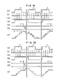
- Fig. 2 shows the waveform of the output signals from the write control circuit 13. Shown by 30, 31 and 32 are control signals for controlling the switch circuit 9, 33 is a control signal for controlling the A/D converter 10, and 34 is a control signal for controlling the latch circuit 11.
- Fig. 3 shows the arrangement including the switch circuit 9, AID converter 10 and latch circuit 11 for latching (holding) only necessary signal portion in response to the latch control signal 34 before the signal is stored in the memory 12.
- switches in the switch circuit 9 become conductive, and the luminance signal (Y) and two color-difference signals (R-Y, B-Y) are conducted sequentially through the A/D converter 10 to the latch circuit 11.
- the A/D converter 10 operates to convert the input signal at the rising edge of the control signal 33.
- the luminance signal is sampled at a frequency four times the color-difference signals which are sampled alternately. Consequently, these signals are converted into time-series data Y, Y, R-Y, Y, Y, B-Y, and so on.
- Fig. 4 shows another arrangement of the same circuit portion, in which data transfer control for the memory (will be described later) is taken into consideration.
- the arrangement includes latches 11-1, 11-2 and 11-3 and switches 43, 44 and 45 which operate in unison. These latches and switches are controlled in a timing relationship shown in Fig. 6 as will be described later.
- the arrangement shown in Fig. 5 includes a first port (memory area) 60, an address controller 61 for designating the write address of data Di supplied on the input port 63, and a second port (output register) 62 of the dual-port memory 12.
- the memory used in this system is a dual-port memory which is prevalent in recent years, and it has its input port 63 and output port 64 controlled independently.
- the memory is written the input date Di in a random access manner, while it is read out in a serial manner.
- the memory operates relatively slower in writing relative to reading, and therefore it is suitable for time-axis compression, such as for "picture-in-picture" display operation.
- Writing into the memory area 60 in the memory 12 is carried out by specifying the address of one location within the memory area.
- the input data Di is written in a cell bm, for example, of the memory area 60 by way of the input port 63.
- a row of data an, bn and so on are transferred from the memory area 60 to the output register 62, and then the set of data are shifted out of the output register in the order of an, bn and so on.
- the address controller 61 specifies a row.
- the memory read/write operations are basically asynchronous. The write operation is suppressed only during the data transfer from the memory area 60 to the output register 62. This necessitates the holding of the input data in the forward latch circuit 11 during the data transfer, but it can be accomplished by the arrangement of Fig. 4.
- Fig. 4 showing the output signal waveforms of the write control circuit 13.
- Shown by 30, 31 and 32 are control signals for controlling the switch circuit 9; 40, 38 and 39 are signals for controlling the latches 11-1, 11-2 and 11-3 in the latch circuit 11 which hold the color-difference signals (R-Y, B-Y), the first luminance signal (Y) and the second luminance signal (Y) provided by the A/D converter 10, respectively, 37, 36 and 37 are control signals for controlling the switches 43-45 which introduce latched data into the memory 12, and 41 is a control signal issued during the data transfer for controlling the memory 12.
- FIG. 6 show the timing of data latch and timing of data output before and after the data transfer.
- the data latched in the latch 11-3 by the control signal 40 is outputted during the "high” period of the control signal 37.
- the data latched in the latches 11-1 and 11-2 in the latch circuit 11 by the control signals 38 and 39 are outputted during the "high” period of the control signals 35 and 36.
- a color-difference signal and two luminance signals are transferred to the memory 12 in the order of R-Y, Y, B-Y, Y, Y, and so on.
- any one of the control signals 37, 35 and 36 coincident with data transfer has its output period extended.
- the output period can be extended up to the time point immediately before the next latching signal comes, and therefore latched data can be transferred in the correct order to the memory 12 without being destructed. Namely, at the data transfer, input data is latched in the latch circuit 11 and writing to the memory 12 is inhibited.
- Fig. 7 shows an example of the latch circuit 15
- Fig. 8 shows the waveforms of the output signal from the memory 12 and the output signal of the read control circuit 14.
- Shown by 80 is a string of data retrieved from the memory 12;
- 82, 83, 86 and 87 are control signals for controlling the latches 15-1 through 15-4 in the latch circuit 15, and
- 84 and 85 are control signals provided by the control circuit 14 for controlling the switches 70 and 71.
- the data string 80 read out of the output register 62 of the memory 12 in response to the clock signal 81 (will be explained later) is held in latches 15-1 through 15-4 in response to the latch control signals 82, 83, 86 and 87.
- the switches 70 and 71 are operated by the control signals 84 and 85.
- the above control operation is implemented by the read control circuit 14 (Fig. 1), and as a whole time-axis compression by use of a dual-port memory is made possible.
- the timing of data transfer is at the end of output of a row (all or part) of data from the output register 62 of the memory 12, or at a time point when the need of transfer of the next row of data from the memory area 60 to the output register 62.
- a timing of data transfer for time domain near the horizontal sync signal in the sub-field video signal is not suitable by the following reasons.
- the read clock is used for memory access control only during the data transfer.
- the difference in the phase of the read and write clocks makes it very difficult the switching of control for the usual writing controlled by the write control and the data transfer controlled by the read clock.
- a control system having a data transfer timing out of phase with the horizontal sync for writing is desired.
- Fig. 9 shows in block diagram the arrangement of the data transfer timing signal extractor (shown by 180 in Fig. 1) which meets the above requirement
- Fig. 10 shows the waveforms of the principal signals observed in the circuit.
- the arrangement includes a write clock generator 100, a write horizontal sync separator 101, a write address counter 102, a data transfer inhibitor 103, a read clock generator 104, a read horizontal sync separator 105, a read address counter 106, a data transfer trigger generator 107, an inverter 108, an AND gate 109., a data transfer signal generator 110, and an image read period signal generator 111.
- the write address counter 102 is preset in response to the horizontal sync signal 120 extracted by the write horizontal sync separator 101.
- the counter 102 counts the clock produced by the write clock generator 100 to setup a data transfer period (pulse signal 121) before and after the horizontal sync signal.
- the pulse formation is achieved by the logical operations for the count of the address counter by the data transfer inhibitor 103. For example, when the counter 102 contains "5" and "200" at time points indicated by the dashed lines 400 and 401 in Fig. 10, the inhibitor 103 reveals the period where the count is larger than 200 and the period where the count is smaller than 5.
- the read address counter 106 which counts synchronously with the read horizontal sync signal (not shown) provides a read period signal 124 for the sub-field video signal through the image read period signal generator 111, a data transfer trigger signal 122 is obtained in other time domain (outside of the read period) by the data transfer trigger generator 107, and the process for the signals 121 and 122 by the inverter 108 and AND gate 109 yields a signal 123, which operates on the data transfer signal generator 110 to produce a data transfer timing signal 125.
- the read period for the sub-field video signal is determined by the image readout period generator 111, e.g., when the counter 106 contains a value which is smaller than 100 and larger than 150 it is determined that the sub-field video signal is being read out.
- the functional blocks 100-102 and 104-106 are incorporated in the data transfer timing signal extractor 180, the blocks 100-102 may be incorporated in the write control circuit 13 and the blocks 104-106 and 111 may be incorporated in the read control circuit 14.
- Fig. 11 shows in block diagram the image processing system representing another embodiment of this invention.
- This embodiment is capable of accomplishing "picture-in-picture" for the sub-field with high picture equality using only one memory.
- the disturbance in sub-field which is caused by the outrun of the memory read phase over the memory write phase i.e.. the misalignment of sub-field video signals (2-field display) read out of the memory, can be prevented.
- the embodiment will be described in detail with reference to the drawing.
- Fig. 11 the same portions as of the preceding embodiment shown in Fig. 1 are referred by the same symbols and the explanation thereof will be omitted.
- Shown by 301 and 302 are sync separation circuits connected to the first and second video signal sources for separating the vertical and horizontal sync signals from the video signal.
- 303 and 304 are field discriminating circuits for discriminating the field of the main-field video signal by receiving the sync signals, 304 is a false operation preventing circuit, 3' and 4' are switches operated in unison and connected to the outputs of the field discriminating circuits 303 and 304;
- 306 is a field information read/write outrun inhibit circuit which receives the sigal passing the switches and produces a control signal for controlling the switching control circuit 5 and a control signal for controlling the dual-port memory 12 in the time-axis compressing circuit in the video signal processing unit 220, and a television receiver set 16.
- the video signals including the main-field video signal and sub-field video signal originating from the video signal sources 1 and 2 are fed to the sync separating circuits 301 and 302, respectively, by which the vertical sync signal and horizontal sync signal are separated.
- the video signals are further fed through the field discriminating circuits 303 and 304 and switched 3' and 4', and supplied to the outrun inhibit circuit 306.
- the main-field video signal from the video signal source 2 is fed through the switch 3 to one input terminal of an adder 26.
- the sub-field video signal from the video signal source 1 is fed through the switch 4 to the memory 12, and after it is compressed on the time-axis by the memory it is delivered to another input terminal of the adder 26.
- the main and sub-field video signals merged by the adder 26 are delivered to the television receiver set 16, on which two fields are displayed to accomplish the "picture-in-picture" function.
- the false operation preventing circuit 305 and switching control circuit 5 play a protective role for coping with the field discrimination for the sync signals disturbed by noises and the transitional operation at exchange of two fields, and these circuits may be simplified or eliminated in some cases.
- Figs. 12 and 13 are block diagrams for explaining the read/write operations of the memory 12. Shown in Fig. 12 by 10a is an analog-to-digital (A/D) converter, 10b is a sampling circuit, 10c is an automatic phase controller, 10d is a clock signal generator, 11 a and 15a are switches, 60a-60d are areas of a memory 12, and 19 is a digital-to-analog (D/A) converter.
- the sub-field video signal S1 in a digital form at the end of the A/D converter 10a is sampled by the sampling circuit 10b in response to the clock signal provided by the clock signal generator 10d.
- the clock signal is controlled by the automatic phase controller 10c to be in-phase with the burst signal of the sub-field video signal S1, and it has a frequency twice or more of the burst signal.
- the sampled signal is written into any of the areas 60a-60d in the memory 12.
- the memory readout operation takes place in asynchronous manner with the write operation.
- the memory read and write operations are carried out by switching the switches 11 a and 15a by the control signal C (C1 and C2) from the outrun inhibit circuit 306 based on the result of field discrimination by the field discriminating circuits 301 and 302. Transforming the signal read out of the memory areas 60a-60d into an analog signal by the D/A converter 19 results in a signal S1' which is a time-axis compressed version of the sub-field video signal S1.
- Fig. 13 Shown in Fig. 13 by 6 is a luminance signal extractor, 8 is a color-difference separator, 8' is an automatic phase synchronization control circuit, 9 and 19d are switches, 10e is a color-difference and luminance switching circuit, 19a'and 19b are D/A converters, and 19c is an adder.
- the difference between Fig. 12 and Fig. 13 is whether or not the sub-field video signal S1 is decomposed into the luminance signal and color-difference signal.
- the former can be called “composite system", and the latter "component system".
- the automatic phase synchronization control circuit 42 is used for the control.
- the circuit is known in the art and its detailed explanation will be omitted.
- the color signal separator 8 is merely required to demodulate the color-difference signal from the NTSC signal, and a commonly used demodulator suffices for this purpose.
- the luminance signal is extracted by the luminance signal extractor 6, and also in this case a usual low-pass filter suffices for the purpose.
- the input signal which has been decomposed into the luminance signal and color-difference signal is fed through the switch 9 to the A/D converter 10a, by which it is transformed into digital data in a time slicing manner. After that the data is stored in the memory areas 60a-60d by way of the sampling circuit 10b and switch 11a.
- This management of the signal is due to the use of a single A/D converter, and in exchange for the provision of a plurality of A/D converters the switch circuits 9 and 19d and the color-difference and luminance switching circuit 10e can be eliminated.
- the switch 19d In synchronism with the clock signal produced by the clock signal generator 10d, the switch 19d is operated by the signal C4 and at the same time sampling is implemented by the sampling circuit 10b. Accordingly, when the switch 19d is positioned to a -terminal, the luminance signal is A/D converted and sampled by the samping circuit 10b and then written in the memory areas 60a-60d. With the switch 19d positioned to -terminal the color-difference signal is sampled and written in the memory areas 60a-60d. For reading, the switch 19d is operated in synchronism with the reading of the memory areas 60a-60d.
- the read clock is controlled by the color-difference and luminance switching circuit 10e so that the luminance and color-difference signals are read out in a prescribed order, and the witch 19d is operated at this timing.
- the switch 19d is positioned to G)-terminal at reading of the luminance signal out of the memory areas, while the switch is positioned to b -terminal at reading of the color-difference signal, and after being transformed into analog signals by the D/A converters 19a and 19b both signals are merged by the adder 19c.
- This summing operation implies modulation to the NTSC signal, and a usual NTSC modulator suffices for the purpose.
- Fig. 14 shows in block diagram the arrangment of the outrun inhibit circuit 306
- Fig. 15 explains the circuit
- Fig. 17 is a waveform diagram used to explain the operation of the circuit.
- 306a is an AND gate
- 306b is a sub-field trigger generator
- 306c and 306d are flip-flops
- 306e and 306f are decoders.
- Fig. 15 shown by 16a and 16b are screens on the Braun tube of the television receiver set.
- Figs. 16 and 17, shown by T1 through T17 are time bands on the signal waveforms.
- the main-field and sub-field discrimination signals f1 and f2 are the input signals to the outrun inhibit circuit 306.
- the field discrimination signal f2 for the sub-field is divided in frequency by two by the flip-flop 306d, which produces a signal 60 on its Q-output.
- the field discrimination signal (information) f1 for the main-field is taken AND by the AND gate 306a with the sub-field trigger signal 61 produced by the sub-field trigger generator 306b.
- the sub-field trigger signal 61 is a pulse which rises when the scanning spot has reached a point al on the screen 16a (see Fig. 15), and it indicates the starting time point for the sub-field display (the falling time point is arbitrary).
- the resulting signal 62 is used as a data input trigger for the flip-flop 306c.
- the flip-flop 306c has its input terminal D receiving a signal 60 which is the result of frequency division for the signal f2 by the flip-flop 306d, and therefore the flip-flop 306c produces a signal 63 on its Q -output.
- Table 1 lists the states of the signal f2 and signal 60 in the time bands T1 and T4 and the signal f1 and signal 63 in the time bands T5-T9.
- the time difference between reading and writing of a memory area is greater than 1-field scanning length.
- the time difference between reading and writing is short, but in this case reading always precedes writing for a memory area. For example, at time t1 in Fig.
- the signal f2 and signal 60 are both low, causing the write switch 11a to position to c-terminal, as indicated in Table 3, while the signal f1 and signal 63 are both high, causing the switch 11 a to turn to b-terminal.
- the b1 information for the screen 18b is written in the memory, but in this case reading takes place for the memory area 60d are writing takes place for the memory area 60c.
- the signals f2 and 60 go high, causing the switch 11a to turn to@ -terminal.
- Reading and writing take place for the same memory area 60c, but in the time band T5 reading for the memory area 60c always precedes, and therefore the writing phase never outruns the reading phase. Reading of the memory area 60c completes at time t3, and a short while later following the end of the time band T1, writing of the memory area 60c completes. For the same memory area, the reading phase and writing phase becomes closest when the signals f2, 60 and 63 rise coincidently (at this time the signal f1 is fixed to high), but even under this condition reading always precedes writing except for a coincident moment at the beginning of reading and writing for a memory area. Accordingly, the outrun phenomenon can be prevented by the present invention.
- 303a is a horizontal sync separator
- 303b is a vertical sync separator
- 303c is a pulse generating circuit
- 303d is a reversible counter
- 303e is a logic circuit
- 303f is a flip-flop
- 305a is a frequency division counter
- 305b is a discrimination circuit.
- Shown by 134 is a preset pulse applied to the reversible counter 303d
- 135 is a latching pulse for the output of the reversible counter 303d.
- the sync-separated signal 130 is fed to the horizontal sync separator 303a and vertical sync separator 303b, by which a horizontal sync signal 131 and vertical sync signal 132 are extracted.
- the number of pulses of the horizontal sync signal 131 in the outside of the period of the vertical sync signal 132 varies in each field, and the number of pulses of the horizontal sync signal within the vertical sync signal period (a, b, c) also varies in each field.
- the pulse generating circuit 303c extracts horizontal sync pulses 133 within the vertical sync periods a, b and c, and supplies them as a clock to the reversible counter 303d.
- the reversible counter 303d reveals the difference of horizontal sync pulses 133 among the consecutive vertical sync periods a, b and c. Namely, the circuit bases the field discriminations of the difference of horizontal sync pulses 133 in consecutive vertical sync periods.
- the flip-flop 303f doubles the period of the vertical sync signal 132, and the first horizontal sync pulse (e) during the high period of that vertical sync signal and following the falling of the original vertical sync signal is used to make a latching pulse 134, and the subsequent horizontal sync pulse (d) is used to make a presetting pulse 135.
- the reversible counter 303d is made up of three bits having bit outputs Q1, Q2 and Q3, and the counter is preset to have '111' on the Q1, Q2 and Q3, i.e., a preset value of 7.
- the reversible counter 303d is designed to up-count in response to a high output signal (f1) from the flip-flop 303f and down-count in response to a low output signal f1. Under these operating conditions, the reversible counter 303d which has been preset to value 'T in response to the preset pulse 135 at time point d operates to down-count (because of the low signal 136) the horizontal sync pulses 133 within the period of the next vertical sync signal 132. Accordingly. the counter 303d down-counts from 7 to '6' to '5' and to '4' as shown by 137 in Fig. 19, and in the next vertical sync period c up-counts the pulses 133 from '5' to '6' to 7 and to '0'. The count value is latched in response to the latch pulse 134 at e.
- the latched count value is rendered zero.
- the latched count value when the signal 136 goes low in the period (b) including a larger number of horizontal sync pulses is 7.
- the above latching operation and discrimination of the count value are the role of the logic circuit 303e, and it suffices to determine whether the latched value of Q3 is high or low.
- the false operation preventing circuit 305 is provided for this purpose, and it includes a decision circuit 305b which makes a final decision upon consistent results of count for the vertical sync signal 132 (or signal 136) by the counter 305a.
- the flip-flop 303f is controlled to reverse upon successive false decisions in several count operations, and the noise immunity of the operation can be enhanced significantly.
- the switching control circuit 5 in Figs. 11 and 12 serves to exchange the main-field and sub-field in 2-field display.
- the circuit is operated in synchronism with the vertical sync signal to gain the smoothness. Since the circuit can be arranged using known means, and its detailed explanation will be omitted.
Landscapes
- Engineering & Computer Science (AREA)
- Multimedia (AREA)
- Signal Processing (AREA)
- Television Signal Processing For Recording (AREA)
- Studio Circuits (AREA)
- Television Systems (AREA)
- Synchronizing For Television (AREA)
Applications Claiming Priority (4)
| Application Number | Priority Date | Filing Date | Title |
|---|---|---|---|
| JP61106609A JPS62264775A (ja) | 1986-05-12 | 1986-05-12 | 画像処理装置 |
| JP106609/86 | 1986-05-12 | ||
| JP112604/86 | 1986-05-19 | ||
| JP11260486A JPH07101931B2 (ja) | 1986-05-19 | 1986-05-19 | 画像処理装置 |
Publications (3)
| Publication Number | Publication Date |
|---|---|
| EP0245745A2 true EP0245745A2 (fr) | 1987-11-19 |
| EP0245745A3 EP0245745A3 (en) | 1989-03-15 |
| EP0245745B1 EP0245745B1 (fr) | 1993-10-27 |
Family
ID=26446737
Family Applications (1)
| Application Number | Title | Priority Date | Filing Date |
|---|---|---|---|
| EP87106443A Expired - Lifetime EP0245745B1 (fr) | 1986-05-12 | 1987-05-04 | Système de traitement d'image |
Country Status (4)
| Country | Link |
|---|---|
| US (1) | US4984083A (fr) |
| EP (1) | EP0245745B1 (fr) |
| KR (1) | KR910001654B1 (fr) |
| DE (1) | DE3787923T2 (fr) |
Cited By (5)
| Publication number | Priority date | Publication date | Assignee | Title |
|---|---|---|---|---|
| GB2221593A (en) * | 1988-07-08 | 1990-02-07 | Samsung Electronics Co Ltd | An image signal processing circuit for producing multiple pictures on a common display screen |
| GB2236031A (en) * | 1989-06-30 | 1991-03-20 | Samuelson Group Plc | Video mixer and special effects unit |
| GB2201317B (en) * | 1987-02-17 | 1991-07-17 | Rca Licensing Corp | Picture-in-picture video signal generator |
| EP0533748A4 (en) * | 1990-06-01 | 1993-11-24 | Thomson Consumer Electronics, Inc. | Field synchronization system maintaining interlace integrity |
| EP0772357A3 (fr) * | 1995-09-08 | 1998-04-15 | Matsushita Electric Industrial Co., Ltd. | Dispositif d'affichage vidéo pour l'affichage simultané de plusieurs images sur un écran |
Families Citing this family (16)
| Publication number | Priority date | Publication date | Assignee | Title |
|---|---|---|---|---|
| JP2973420B2 (ja) * | 1988-03-30 | 1999-11-08 | キヤノン株式会社 | ビデオ・カメラ |
| US5208660A (en) * | 1989-07-29 | 1993-05-04 | Sharp Kabushiki Kaisha | Television display apparatus having picture-in-picture display function and the method of operating the same |
| KR910013904A (ko) * | 1989-12-21 | 1991-08-08 | 강진구 | Hd 스크린을 이용한 pop 재생 tv |
| JPH03204283A (ja) * | 1989-12-29 | 1991-09-05 | Nec Corp | 子画面情報記憶回路 |
| US5369444A (en) * | 1990-06-01 | 1994-11-29 | Thomson Consumer Electronics | Field type matching system |
| US5287189A (en) * | 1992-08-21 | 1994-02-15 | Thomson Consumer Electronics, Inc. | Displaying an interlaced video signal with a noninterlaced video signal |
| US20040230992A1 (en) * | 1993-05-27 | 2004-11-18 | Gemstar Development Corporation | Method and apparatus for displaying video clips |
| US6002444A (en) | 1994-05-20 | 1999-12-14 | United Video Properties, Inc. | Video clip program guide |
| US5523796A (en) * | 1994-05-20 | 1996-06-04 | Prevue Networks, Inc. | Video clip program guide |
| MY118491A (en) * | 1995-06-02 | 2004-11-30 | Matsushita Electric Industrial Co Ltd | A subpicture image signal vertical compression circuit |
| KR100186409B1 (ko) * | 1996-04-23 | 1999-05-01 | 구자홍 | 피씨와 티브이 적응형 피아이피 영상신호 처리회로 |
| TW374155B (en) * | 1997-05-27 | 1999-11-11 | Sony Corp | Image compression device and image compression method |
| EP1292133A1 (fr) * | 2001-09-06 | 2003-03-12 | Koninklijke Philips Electronics N.V. | Affichage à images multiples |
| KR100463531B1 (ko) * | 2002-10-11 | 2004-12-29 | 엘지전자 주식회사 | 디지털 tv의 주/부화면 처리 장치 |
| JP5672862B2 (ja) | 2010-08-27 | 2015-02-18 | ソニー株式会社 | 撮像装置、撮像システム及び撮像方法 |
| KR101573916B1 (ko) * | 2014-12-16 | 2015-12-02 | (주)넥스트칩 | 영상 수신 방법 및 장치 |
Family Cites Families (11)
| Publication number | Priority date | Publication date | Assignee | Title |
|---|---|---|---|---|
| GB1576621A (en) * | 1976-03-19 | 1980-10-08 | Rca Corp | Television synchronizing apparatus |
| DE2644706C3 (de) * | 1976-10-04 | 1985-12-05 | Robert Bosch Gmbh, 7000 Stuttgart | System zur Übertragung bzw. Speicherung eines Farbfernsehsignals |
| DE2725362C3 (de) * | 1977-06-04 | 1980-08-28 | Robert Bosch Gmbh, 7000 Stuttgart | Verfahren zum Verarbeiten von Farbfernsehsignalen |
| JPS5492015A (en) * | 1977-12-29 | 1979-07-20 | Matsushita Electric Ind Co Ltd | Color television image receiving unit |
| JPS6053940B2 (ja) * | 1978-05-19 | 1985-11-28 | 株式会社東京放送 | フレ−ムシンクロナイザにおける書き込み禁止制御回路 |
| US4249213A (en) * | 1978-09-14 | 1981-02-03 | Hitachi, Ltd. | Picture-in-picture television receiver |
| JPS5637778A (en) * | 1979-09-04 | 1981-04-11 | Sony Corp | Producing circuit of inserted screen signal |
| US4562435A (en) * | 1982-09-29 | 1985-12-31 | Texas Instruments Incorporated | Video display system using serial/parallel access memories |
| US4623915A (en) * | 1984-09-21 | 1986-11-18 | Rca Corporation | Apparatus for processing multiple time division multiplexed asynchronous composite video signals |
| US4656515A (en) * | 1985-03-25 | 1987-04-07 | Rca Corporation | Horizontal compression of pixels in a reduced-size video image utilizing cooperating subsampling and display rates |
| US4665438A (en) * | 1986-01-03 | 1987-05-12 | North American Philips Corporation | Picture-in-picture color television receiver |
-
1987
- 1987-05-04 DE DE3787923T patent/DE3787923T2/de not_active Expired - Fee Related
- 1987-05-04 EP EP87106443A patent/EP0245745B1/fr not_active Expired - Lifetime
- 1987-05-07 KR KR1019870004461A patent/KR910001654B1/ko not_active Expired
-
1989
- 1989-06-28 US US07/373,630 patent/US4984083A/en not_active Expired - Lifetime
Cited By (7)
| Publication number | Priority date | Publication date | Assignee | Title |
|---|---|---|---|---|
| GB2201317B (en) * | 1987-02-17 | 1991-07-17 | Rca Licensing Corp | Picture-in-picture video signal generator |
| GB2221593A (en) * | 1988-07-08 | 1990-02-07 | Samsung Electronics Co Ltd | An image signal processing circuit for producing multiple pictures on a common display screen |
| GB2221593B (en) * | 1988-07-08 | 1993-01-06 | Samsung Electronics Co Ltd | An image signal processing circuit for producing mulitple pictures on a common display screen |
| GB2236031A (en) * | 1989-06-30 | 1991-03-20 | Samuelson Group Plc | Video mixer and special effects unit |
| GB2236031B (en) * | 1989-06-30 | 1993-11-17 | Samuelson Group Plc | Video mixer unit |
| EP0533748A4 (en) * | 1990-06-01 | 1993-11-24 | Thomson Consumer Electronics, Inc. | Field synchronization system maintaining interlace integrity |
| EP0772357A3 (fr) * | 1995-09-08 | 1998-04-15 | Matsushita Electric Industrial Co., Ltd. | Dispositif d'affichage vidéo pour l'affichage simultané de plusieurs images sur un écran |
Also Published As
| Publication number | Publication date |
|---|---|
| KR910001654B1 (ko) | 1991-03-16 |
| US4984083A (en) | 1991-01-08 |
| DE3787923D1 (de) | 1993-12-02 |
| KR870011790A (ko) | 1987-12-26 |
| DE3787923T2 (de) | 1994-05-26 |
| EP0245745A3 (en) | 1989-03-15 |
| EP0245745B1 (fr) | 1993-10-27 |
Similar Documents
| Publication | Publication Date | Title |
|---|---|---|
| US4984083A (en) | Image processing system | |
| US4364090A (en) | Method for a compatible increase in resolution in television systems | |
| US4249213A (en) | Picture-in-picture television receiver | |
| GB2090505A (en) | Television receivers | |
| JP2756675B2 (ja) | ピクチャーインピクチャーのビデオ信号発生回路 | |
| US4673983A (en) | Picture-in-picture television receivers | |
| US5070395A (en) | Television signal system conversion apparatus | |
| DK166339B (da) | Videofremvisningsanlaeg til fremvisning af videosignaler med stort og standard formatforhold | |
| US4821086A (en) | TV receiver having in-memory switching signal | |
| JP2852743B2 (ja) | テレビジョン信号処理回路 | |
| GB2162674A (en) | Color liquid crystal display apparatus with improved display color mixing | |
| US4782391A (en) | Multiple input digital video features processor for TV signals | |
| US5726715A (en) | Method and apparatus for displaying two video pictures simultaneously | |
| HK1000198B (en) | Digital video features processor for tv signals | |
| US6046777A (en) | Apparatus for sampling and displaying an auxiliary image with a main image to eliminate a spatial seam in the auxiliary image during freeze frame operation | |
| US4991013A (en) | Picture-in-picture television apparatus with sync controlled memory addressing | |
| US5309238A (en) | Picture superposing circuit | |
| US4951126A (en) | Video signal processing method and apparatus therefor for creating a picture-in-picture | |
| JPS63123284A (ja) | テレビジヨン受像機 | |
| US4907072A (en) | Mosaic picture generation circuit | |
| JP3407449B2 (ja) | 走査線変換回路 | |
| JP2860988B2 (ja) | 画像記憶装置 | |
| JP3112078B2 (ja) | 画像記憶装置 | |
| JP2681996B2 (ja) | 画像処理装置 | |
| JP3550302B2 (ja) | 往復偏向式映像信号表示装置 |
Legal Events
| Date | Code | Title | Description |
|---|---|---|---|
| PUAI | Public reference made under article 153(3) epc to a published international application that has entered the european phase |
Free format text: ORIGINAL CODE: 0009012 |
|
| 17P | Request for examination filed |
Effective date: 19870504 |
|
| AK | Designated contracting states |
Kind code of ref document: A2 Designated state(s): DE FR GB |
|
| PUAL | Search report despatched |
Free format text: ORIGINAL CODE: 0009013 |
|
| AK | Designated contracting states |
Kind code of ref document: A3 Designated state(s): DE FR GB |
|
| 17Q | First examination report despatched |
Effective date: 19910604 |
|
| GRAA | (expected) grant |
Free format text: ORIGINAL CODE: 0009210 |
|
| AK | Designated contracting states |
Kind code of ref document: B1 Designated state(s): DE FR GB |
|
| REF | Corresponds to: |
Ref document number: 3787923 Country of ref document: DE Date of ref document: 19931202 |
|
| ET | Fr: translation filed | ||
| PLBE | No opposition filed within time limit |
Free format text: ORIGINAL CODE: 0009261 |
|
| STAA | Information on the status of an ep patent application or granted ep patent |
Free format text: STATUS: NO OPPOSITION FILED WITHIN TIME LIMIT |
|
| 26N | No opposition filed | ||
| REG | Reference to a national code |
Ref country code: GB Ref legal event code: IF02 |
|
| PGFP | Annual fee paid to national office [announced via postgrant information from national office to epo] |
Ref country code: FR Payment date: 20030423 Year of fee payment: 17 |
|
| PGFP | Annual fee paid to national office [announced via postgrant information from national office to epo] |
Ref country code: GB Payment date: 20030425 Year of fee payment: 17 |
|
| PGFP | Annual fee paid to national office [announced via postgrant information from national office to epo] |
Ref country code: DE Payment date: 20030605 Year of fee payment: 17 |
|
| PG25 | Lapsed in a contracting state [announced via postgrant information from national office to epo] |
Ref country code: GB Free format text: LAPSE BECAUSE OF NON-PAYMENT OF DUE FEES Effective date: 20040504 |
|
| PG25 | Lapsed in a contracting state [announced via postgrant information from national office to epo] |
Ref country code: DE Free format text: LAPSE BECAUSE OF NON-PAYMENT OF DUE FEES Effective date: 20041201 |
|
| GBPC | Gb: european patent ceased through non-payment of renewal fee |
Effective date: 20040504 |
|
| PG25 | Lapsed in a contracting state [announced via postgrant information from national office to epo] |
Ref country code: FR Free format text: LAPSE BECAUSE OF NON-PAYMENT OF DUE FEES Effective date: 20050131 |
|
| REG | Reference to a national code |
Ref country code: FR Ref legal event code: ST |