EP0240312B1 - Stabilized electric power apparatus for generating direct and alternating current simultaneously in one transformer - Google Patents
Stabilized electric power apparatus for generating direct and alternating current simultaneously in one transformer Download PDFInfo
- Publication number
- EP0240312B1 EP0240312B1 EP87302791A EP87302791A EP0240312B1 EP 0240312 B1 EP0240312 B1 EP 0240312B1 EP 87302791 A EP87302791 A EP 87302791A EP 87302791 A EP87302791 A EP 87302791A EP 0240312 B1 EP0240312 B1 EP 0240312B1
- Authority
- EP
- European Patent Office
- Prior art keywords
- circuit
- power supply
- supply apparatus
- coil
- transformer
- Prior art date
- Legal status (The legal status is an assumption and is not a legal conclusion. Google has not performed a legal analysis and makes no representation as to the accuracy of the status listed.)
- Expired - Lifetime
Links
Images


Classifications
-
- H—ELECTRICITY
- H02—GENERATION; CONVERSION OR DISTRIBUTION OF ELECTRIC POWER
- H02M—APPARATUS FOR CONVERSION BETWEEN AC AND AC, BETWEEN AC AND DC, OR BETWEEN DC AND DC, AND FOR USE WITH MAINS OR SIMILAR POWER SUPPLY SYSTEMS; CONVERSION OF DC OR AC INPUT POWER INTO SURGE OUTPUT POWER; CONTROL OR REGULATION THEREOF
- H02M1/00—Details of apparatus for conversion
- H02M1/42—Circuits or arrangements for compensating for or adjusting power factor in converters or inverters
-
- H—ELECTRICITY
- H05—ELECTRIC TECHNIQUES NOT OTHERWISE PROVIDED FOR
- H05B—ELECTRIC HEATING; ELECTRIC LIGHT SOURCES NOT OTHERWISE PROVIDED FOR; CIRCUIT ARRANGEMENTS FOR ELECTRIC LIGHT SOURCES, IN GENERAL
- H05B41/00—Circuit arrangements or apparatus for igniting or operating discharge lamps
- H05B41/14—Circuit arrangements
- H05B41/26—Circuit arrangements in which the lamp is fed by power derived from dc by means of a converter, e.g. by high-voltage dc
- H05B41/28—Circuit arrangements in which the lamp is fed by power derived from dc by means of a converter, e.g. by high-voltage dc using static converters
- H05B41/282—Circuit arrangements in which the lamp is fed by power derived from dc by means of a converter, e.g. by high-voltage dc using static converters with semiconductor devices
- H05B41/2821—Circuit arrangements in which the lamp is fed by power derived from dc by means of a converter, e.g. by high-voltage dc using static converters with semiconductor devices by means of a single-switch converter or a parallel push-pull converter in the final stage
- H05B41/2824—Circuit arrangements in which the lamp is fed by power derived from dc by means of a converter, e.g. by high-voltage dc using static converters with semiconductor devices by means of a single-switch converter or a parallel push-pull converter in the final stage using control circuits for the switching element
-
- H—ELECTRICITY
- H02—GENERATION; CONVERSION OR DISTRIBUTION OF ELECTRIC POWER
- H02M—APPARATUS FOR CONVERSION BETWEEN AC AND AC, BETWEEN AC AND DC, OR BETWEEN DC AND DC, AND FOR USE WITH MAINS OR SIMILAR POWER SUPPLY SYSTEMS; CONVERSION OF DC OR AC INPUT POWER INTO SURGE OUTPUT POWER; CONTROL OR REGULATION THEREOF
- H02M3/00—Conversion of dc power input into dc power output
- H02M3/02—Conversion of dc power input into dc power output without intermediate conversion into ac
- H02M3/04—Conversion of dc power input into dc power output without intermediate conversion into ac by static converters
- H02M3/10—Conversion of dc power input into dc power output without intermediate conversion into ac by static converters using discharge tubes with control electrode or semiconductor devices with control electrode
- H02M3/145—Conversion of dc power input into dc power output without intermediate conversion into ac by static converters using discharge tubes with control electrode or semiconductor devices with control electrode using devices of a triode or transistor type requiring continuous application of a control signal
- H02M3/155—Conversion of dc power input into dc power output without intermediate conversion into ac by static converters using discharge tubes with control electrode or semiconductor devices with control electrode using devices of a triode or transistor type requiring continuous application of a control signal using semiconductor devices only
-
- H—ELECTRICITY
- H02—GENERATION; CONVERSION OR DISTRIBUTION OF ELECTRIC POWER
- H02M—APPARATUS FOR CONVERSION BETWEEN AC AND AC, BETWEEN AC AND DC, OR BETWEEN DC AND DC, AND FOR USE WITH MAINS OR SIMILAR POWER SUPPLY SYSTEMS; CONVERSION OF DC OR AC INPUT POWER INTO SURGE OUTPUT POWER; CONTROL OR REGULATION THEREOF
- H02M3/00—Conversion of dc power input into dc power output
- H02M3/22—Conversion of dc power input into dc power output with intermediate conversion into ac
- H02M3/24—Conversion of dc power input into dc power output with intermediate conversion into ac by static converters
- H02M3/28—Conversion of dc power input into dc power output with intermediate conversion into ac by static converters using discharge tubes with control electrode or semiconductor devices with control electrode to produce the intermediate ac
- H02M3/325—Conversion of dc power input into dc power output with intermediate conversion into ac by static converters using discharge tubes with control electrode or semiconductor devices with control electrode to produce the intermediate ac using devices of a triode or a transistor type requiring continuous application of a control signal
- H02M3/335—Conversion of dc power input into dc power output with intermediate conversion into ac by static converters using discharge tubes with control electrode or semiconductor devices with control electrode to produce the intermediate ac using devices of a triode or a transistor type requiring continuous application of a control signal using semiconductor devices only
- H02M3/33538—Conversion of dc power input into dc power output with intermediate conversion into ac by static converters using discharge tubes with control electrode or semiconductor devices with control electrode to produce the intermediate ac using devices of a triode or a transistor type requiring continuous application of a control signal using semiconductor devices only of the forward type
- H02M3/33546—Conversion of dc power input into dc power output with intermediate conversion into ac by static converters using discharge tubes with control electrode or semiconductor devices with control electrode to produce the intermediate ac using devices of a triode or a transistor type requiring continuous application of a control signal using semiconductor devices only of the forward type with automatic control of the output voltage or current
-
- H—ELECTRICITY
- H02—GENERATION; CONVERSION OR DISTRIBUTION OF ELECTRIC POWER
- H02M—APPARATUS FOR CONVERSION BETWEEN AC AND AC, BETWEEN AC AND DC, OR BETWEEN DC AND DC, AND FOR USE WITH MAINS OR SIMILAR POWER SUPPLY SYSTEMS; CONVERSION OF DC OR AC INPUT POWER INTO SURGE OUTPUT POWER; CONTROL OR REGULATION THEREOF
- H02M3/00—Conversion of dc power input into dc power output
- H02M3/22—Conversion of dc power input into dc power output with intermediate conversion into ac
- H02M3/24—Conversion of dc power input into dc power output with intermediate conversion into ac by static converters
- H02M3/28—Conversion of dc power input into dc power output with intermediate conversion into ac by static converters using discharge tubes with control electrode or semiconductor devices with control electrode to produce the intermediate ac
- H02M3/325—Conversion of dc power input into dc power output with intermediate conversion into ac by static converters using discharge tubes with control electrode or semiconductor devices with control electrode to produce the intermediate ac using devices of a triode or a transistor type requiring continuous application of a control signal
- H02M3/335—Conversion of dc power input into dc power output with intermediate conversion into ac by static converters using discharge tubes with control electrode or semiconductor devices with control electrode to produce the intermediate ac using devices of a triode or a transistor type requiring continuous application of a control signal using semiconductor devices only
- H02M3/33561—Conversion of dc power input into dc power output with intermediate conversion into ac by static converters using discharge tubes with control electrode or semiconductor devices with control electrode to produce the intermediate ac using devices of a triode or a transistor type requiring continuous application of a control signal using semiconductor devices only having more than one ouput with independent control
-
- H—ELECTRICITY
- H02—GENERATION; CONVERSION OR DISTRIBUTION OF ELECTRIC POWER
- H02M—APPARATUS FOR CONVERSION BETWEEN AC AND AC, BETWEEN AC AND DC, OR BETWEEN DC AND DC, AND FOR USE WITH MAINS OR SIMILAR POWER SUPPLY SYSTEMS; CONVERSION OF DC OR AC INPUT POWER INTO SURGE OUTPUT POWER; CONTROL OR REGULATION THEREOF
- H02M3/00—Conversion of dc power input into dc power output
- H02M3/22—Conversion of dc power input into dc power output with intermediate conversion into ac
- H02M3/24—Conversion of dc power input into dc power output with intermediate conversion into ac by static converters
- H02M3/28—Conversion of dc power input into dc power output with intermediate conversion into ac by static converters using discharge tubes with control electrode or semiconductor devices with control electrode to produce the intermediate ac
- H02M3/325—Conversion of dc power input into dc power output with intermediate conversion into ac by static converters using discharge tubes with control electrode or semiconductor devices with control electrode to produce the intermediate ac using devices of a triode or a transistor type requiring continuous application of a control signal
- H02M3/335—Conversion of dc power input into dc power output with intermediate conversion into ac by static converters using discharge tubes with control electrode or semiconductor devices with control electrode to produce the intermediate ac using devices of a triode or a transistor type requiring continuous application of a control signal using semiconductor devices only
- H02M3/337—Conversion of dc power input into dc power output with intermediate conversion into ac by static converters using discharge tubes with control electrode or semiconductor devices with control electrode to produce the intermediate ac using devices of a triode or a transistor type requiring continuous application of a control signal using semiconductor devices only in push-pull configuration
- H02M3/3376—Conversion of dc power input into dc power output with intermediate conversion into ac by static converters using discharge tubes with control electrode or semiconductor devices with control electrode to produce the intermediate ac using devices of a triode or a transistor type requiring continuous application of a control signal using semiconductor devices only in push-pull configuration with automatic control of output voltage or current
- H02M3/3378—Conversion of dc power input into dc power output with intermediate conversion into ac by static converters using discharge tubes with control electrode or semiconductor devices with control electrode to produce the intermediate ac using devices of a triode or a transistor type requiring continuous application of a control signal using semiconductor devices only in push-pull configuration with automatic control of output voltage or current in a push-pull configuration of the parallel type
-
- Y—GENERAL TAGGING OF NEW TECHNOLOGICAL DEVELOPMENTS; GENERAL TAGGING OF CROSS-SECTIONAL TECHNOLOGIES SPANNING OVER SEVERAL SECTIONS OF THE IPC; TECHNICAL SUBJECTS COVERED BY FORMER USPC CROSS-REFERENCE ART COLLECTIONS [XRACs] AND DIGESTS
- Y10—TECHNICAL SUBJECTS COVERED BY FORMER USPC
- Y10S—TECHNICAL SUBJECTS COVERED BY FORMER USPC CROSS-REFERENCE ART COLLECTIONS [XRACs] AND DIGESTS
- Y10S315/00—Electric lamp and discharge devices: systems
- Y10S315/01—Fluorescent lamp circuits with more than two principle electrodes
-
- Y—GENERAL TAGGING OF NEW TECHNOLOGICAL DEVELOPMENTS; GENERAL TAGGING OF CROSS-SECTIONAL TECHNOLOGIES SPANNING OVER SEVERAL SECTIONS OF THE IPC; TECHNICAL SUBJECTS COVERED BY FORMER USPC CROSS-REFERENCE ART COLLECTIONS [XRACs] AND DIGESTS
- Y10—TECHNICAL SUBJECTS COVERED BY FORMER USPC
- Y10S—TECHNICAL SUBJECTS COVERED BY FORMER USPC CROSS-REFERENCE ART COLLECTIONS [XRACs] AND DIGESTS
- Y10S315/00—Electric lamp and discharge devices: systems
- Y10S315/07—Starting and control circuits for gas discharge lamp using transistors
Definitions
- the present invention relates to a stabilized electric apparatus which can supply direct and alternating current simultaneously to the load in one transformer and can be used for facsimile optical character readers (referred as OCR hereinafter).
- OCR facsimile optical character readers
- the apparatus shown in Fig. 25 has been known as a multi-output stabilized power supply apparatus used for facsimile, OCR and so on.
- V0 denotes a direct current power supply
- Q1 denotes the transistor for switching
- T1 denotes the inverter transformer
- N p denotes the primary coil
- D1 and D2 denote diodes for rectification
- C1 denotes the capacitor for smoothing
- L1 denotes the choke coil.
- INV denotes the inverter which outputs the alternating current by switching the voltage V1
- T2 denotes the transformer for transforming the alternating current outputted from INV
- C2 denotes the condenser for filter
- Rl denotes the alternating load.
- A1 denotes the error amplifier circuit for comparing the direct output V1 with a reference input voltage V R and outputs the signal corresponding to the difference
- PWM denotes the pulse width modulation circuit which outputs a pulse modulation width, corresponding to the cross-point of signals outputted from the error amplification circuit A1 and triangular waves outputted from the oscillation circuit OSC
- DR denotes the drive circuit which amplifies the pulse and loads it into the base of the transistor Q1.
- the amount of the current flowing in the alternating load Rl is detected by resistance R s and the signal in accordance with the amount is fed back in the inverter INV.
- the inverter INV changes the switching timing of voltage V1 and operates to make the current to be constant.
- the stabilized electric power apparatus should have two sets of switching circuits such as a switching transistor Q1 and an inverter INV, and in addition, two sets of transformers T1 and T2, therefore, the arrangement of the circuit is complicated, on requiring a large number of component parts. As a result, there has been raised a problem of a high manufacturing cost of the stabilized electric power apparatus.
- the alternating load Rl is a fluorescent lamp and used as the luminous source of an image sensor. Since the luminous source of an image sensor is required to have less flicker, so it is necessary to be lighted in a higher frequency.
- alternating current to be outputted shall meet the following requirements
- EP-A-189680 (Articles 56 and 54(3) EPC) discloses a stabilized electric power apparatus in which the oscillator OSC does not oscillate at a constant frequency and the frequency of the oscillator OSC changes in accordance with an alternating current (AC) output voltage of the resistor R s .
- AC alternating current
- the first comparator A1 compares the direct current (DC) output voltage V1 with the reference voltage V R1
- the second comparator A2 compares a voltage applied to the resistor R S with the reference voltage V R2 .
- the oscillating frequency of the oscillator OSC changes in accordance with the output of the second comparator A2.
- the pulse width modulator PM supplies a signal, whose pulse width and frequency are changed in accordance with the outputs of the second comparator A2 and the oscillator OSC, to the transistor Q1 through the drive circuit DR.
- a signal, whose pulse width and frequency are changed, is applied to the switching transistor Q1 so that the DC voltage V1 is kept constant and a current, which flows through the AC load RL, is controlled to be constant.
- impedance means is connected to a coil for generating an AC in a stabilized power supply apparatus of flyback, push-pull, or half-bridge type.
- An object of the present invention is to provide an improved power apparatus for taking out alternating current power and direct current power from voltage created in secondary windings of a transformer, which allows an alternating current load having a negative resistance characteristic to be connected to a direct current power source.
- a stabilized power supply apparatus comprising: a switching circuit for converting a direct current power into pulses by switching, a transformer having a primary winding to be applied with the pulses generated by the switching circuit, at least one first secondary winding and a second secondary winding, a rectifying/smoothing circuit connected to the first secondary winding, an alternating current load connected to the second secondary winding, an oscillator, a comparison circuit for comparing the output of the rectifying/smoothing circuit with a reference value, a pulse width modulator for modulating the pulse width of the output of the oscillator in accordance with the output of the comparison circuit, and a drive circuit for controlling the switching circuit in accordance with the output of the pulse width modulator, characterized in that the alternating current load is connected to the second secondary winding via impedance means, the AC load having negative resistance property, and in that the oscillator oscillates at a constant frequency.
- a stabilized power supply apparatus comprising: a switching circuit for converting a direct current power into pulses by switching, a transformer having a primary winding to be applied with the pulses generated by the switching circuit, at least one first secondary winding a second secondary winding and a third secondary winding, a rectifying/smoothing circuit connected to the first secondary winding, an alternating current load connected to the second secondary winding, a second rectifying/smoothing circuit connected to the third secondary winding, an oscillator, a comparison circuit for comparing a direct voltage derived from an AC voltage across the third secondary winding of the transformer with a reference value, a pulse width modulator for modulating the pulse width of the output of the oscillator in accordance with the output of the comparison circuit, and a drive circuit for controlling the switching circuit in accordance with the output of the pulse width modulator, characterized in that the alternating current load is connected to the second secondary winding via impedance means, the AC load having negative resistance property,
- stabilized alternating current power can be fed to an alternating current load having a negative resistance characteristic.
- Fig. 1 is a circuit diagram showing an embodiment of the stabilized power supply apparatus of the present invention.
- the reference numerals in Fig. 1 are similar to those in Fig. 25.
- the present embodiment is applied to a fly-back converter.
- V0 denotes a direct current power supply
- Q1 denotes a transistor for switching
- T3 denotes a transformer for fly-back converter
- N p denotes a primary coil
- N S1 and N sm denote the secondary coils for direct current output magnetically coupled with the primary coil
- N S2 denotes the secondary coil for alternating current output magnetically combined with the primary coil N p .
- D1 and D m denote diodes for rectifying the second coils N S1 and N sm
- C1 denotes a capacitor for smoothing
- L2 denotes a choke coil provided with the secondary coil N S2 connected in series
- C3 denotes a capacitor connected in series with choke coil L1 for filters
- K b denotes a relay contact provided with alternating current output lines connected in parallel
- Rl denotes an alternating current load.
- A1 denotes an error amplifying circuit which compares the direct current outputted by the secondary coil N S1 with the reference voltage V R1 and outputs signals, depending on the difference (the electric power is supplied from the direct current output V1)
- PC denotes a photo coupler
- R denotes a resistance for electric current control
- OSC denotes an oscillation circuit generating triangular waves
- PWM denotes a pulse width modulating circuit which compares signals outputted by the error amplification circuit A1 with triangular waves outputted by the oscillation circuit OSC and outputs a pulse so that the pulse width can be changed, depending on the movement or the cross-point of both signals
- DR denotes a drive circuit which amplifies the pulse and adds the base of the switching transistor Q1.
- the energy is accumulated in the transformer T3 during the period T on in which transistor Q1 is ON. And the energy accumulated in the transformer T3 is supplied to the direct and alternating current load through N s2 and N sm .
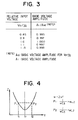
- Fig. 2 shows the relationship between the ON/OFF of the collector current Ic of a transistor Q1 and a voltage E2 created in a secondary coil NS2.
- the value of the voltage E0 during turn-off of the transistor Q1 is the sum of voltages induced by the magnetic coupling between secondary coils NS1, ..., NS n1 creating direct current output powers and a secondary coil Nsp.
- the forward type converter show in Fig. 1, as a forward type converter in which the transformer T3 has m secondary coils NS1 ... NS m and a secondary coil NS2, and creates one alternating current output V2 and one direct current output V1.
- a feedback circuit for stabilizing the direct current output V1 is provided.
- An impedance circuit Z connected to the secondary coil NS2 has two roles of serving as a filter for extracting a fundamental wave component alone from the alternating current output E2 and of stabilizing electrical current when the alternating current load Rl is connected to the secondary coil NS2. At first the role of serving as a filter owned by the impedance circuit Z will be explained.
- Fig. 4 shows the relation between an input impedance Z of the impedance circuit Z and frequency f when viewing an alternating current load Rl from the secondary coil N s2 side.
- fr 1/2 ⁇ ⁇ 1 ⁇ L2 C3 ⁇ ⁇
- the high harmonic wave current supplied in the distribution line of the alternating current load Rl brings about noise and exerts a bad influence on the power source, logic and other electronic circuit which are susceptible to interference electromagnetic fields.
- the alternating current load Rl is an electric discharge lamp such as a fluorescent lamp
- the alternating current load has a negative resistance characteristic which offers such a phenomenon that voltage created in the load is decreased as current running through the load is increased while voltage created in the load is increased as current running through the load is decreased.
- the load current is increased from such a condition that the alternating current V2 is stabilized
- the load voltage V2 is lowered.
- a difference is obtained between the alternating current output E2 and the load voltage V2 and therefore, the load current is further increased.
- the increase in the load current further lowers the load voltage V2 so that it is impossible to restrain the load current from increasing, resulting in damage of the circuit.
- the impedance circuit Z absorbs the difference between the load voltage V2 and the alternating current output E2, which is effected when the load current varies, and therefore, suppresses variations in the load current to a small value. Accordingly, the impedance circuit Z has to have an impedance to some degree.
- the switching frequency (basic wave frequency) of the switching transistor Q1 is set to a frequency f1 or f2 which is slightly shifted from the resonance frequency fr of the impedance circuit Z. Since the frequency of the basic wave is shifted from the resonance frequency fr, it is expected that the fundamental wave component of the alternating output voltage E2 is delayed or superfluous frequency components are taken out. However, the impedance circuit Z attenuates a high frequency wave having a frequency which is n times as large as the frequency of the fundamental wave component where n is an interger, and therefore, there is raised no problem if a shift from the resonance frequency can be restrained below the frequency fr.
- the choke coil L2 and the condenser C3 can be used as stabilizers for the fluorescent lamp current.
- the relay contact K b connected with the Rl in parallel can start the fluorescent lamp
- the number of turns of coil N s2 is defined so that E2 becomes higher than the discharge starting voltage of the fluorescent lamp. Consequently, when the joint K b is opened, the fluorescent lamp starts discharging.
- the constant current can be flowed in setting the switching frequency of the transistor Q1 by connecting the secondary coil N s2 with the impedance circuit Z composed of choke coil L2 and the capacitor C2, without influences of input voltage and changes in the load.
- variable power supply circuit with alternating circuit to transformer T3 and by connecting the alternating output circuit with impedance Z.
- control voltage for stabilizing the output voltage is obtained from the coil N F provided with transformer T3 in case the apparatus is applied to the fly-back converter.
- D s is a rectifier
- C s is a condenser and others are similar to Fig. 1.
- This embodiment shows that a photo-coupler for insulating the primary and the secondary coils are unnecessary.
- PR1 ⁇ PR k shows the positions where a magnetic amplifier or a phase control circuit should optionally be provided (feed-back signals are obtained from the output V k ).
- PR1' ⁇ PR k ' also shows the positions where a series-pass regulator and so on should optionally be provided.
- This embodiment shows the present invention when it is applied to a forward converter.
- V o denotes the direct current power supply
- Q1 denotes the switching transistor
- T3 denotes the inverter transformer
- N p denotes the primary coil
- N s1 denotes the secondary coil for direct current output magnetically combined with the first coil N p
- N s2 denotes the secondary coil for alternating current output magnetically combined with the first coil N p
- D1 and D2 denote the diodes for rectification of the secondary coil N s1
- L1 denotes the choke coil connected with the secondary coil N s1
- C1 denotes the capacitor for smoothing
- L2 denotes the choke coil of the secondary coil N s2
- C3 denotes the capacitor for filter
- K b denotes the relay joint
- Rl denotes the alternating current load (fluorescent lamp).
- A1 denotes the error amplification circuit which compares direct current outputted by the secondary coil N s1 with the standard voltage VR1 and outputs signals depending on the difference
- OSC denotes the oscillation circuit which generates triangular waves
- PWM denotes the pulse width modulation circuit to output a pulse whose width changes, corresponding to the movement of the cross-point
- DR denotes the drive circuit which amplifies the pulse and adds it to the base of the Transistor Q1
- the direct output voltage is stabilized by controlling the duty factor of the transistor Q1.
- the negative half-wave cannot obtain the energy from the input when the transistor Q1 is OFF.
- the voltage of the negative half-wave is made by the exciting energy of the transformer T3, and the magnetic and electrostatic energy are accumulated by the choke coil L2 and capacitor C3 at the end or the positive period.
- an air gap is provided in the magnetic flux path and the exciting energy is enlarged so that the electric power of the coil N s2 necessary for the period of the half-wave can be maintained.
- the excess energy is accumulated by the choke coil and the capacitor C3 at the end of the negative period again, part of which is consumed by a snubber circuit SN provided with the primary coil during the negative period (by a snubber circuit, which is composed of capacitor, resistance and coil provided for reducing stress with the transistor).
- the reset coil N p3 may be combined with the first coil N p1 and provided so that energy can be returned to the input line through the reset coil N p3 .
- the switching circuit on the primary coil N p1 side of the transformer T3 is a 2-transistor type such as a push-pull type or a half-bridge type
- the energy of positive and negative half waves can be supplied from the input by alternately turning two transistors ON.
- the diodes D3 and D4 are used for returning the energy of the alternating current to input side.
- phase angle of electric current i of the secondary coil N s2 is shifted to right or left by the value of the choke coil L2 and condenser C3, on the basis ON-time of transistor Q1.
- Fig. 9 is showing the above-mentioned electric current i.
- the returning amount and a diode being ON vary depending on the value of the choke coil L2, capacitor C3 and resistor R and ON-time width (controlled by PWM) of transistors Q1 and Q2.
- the operation of the impedance circuit Z installed in the secondary coil N s2 is same as the impedance circuit Z shown in Fig. 1.
- the dispersion of the impedance Z can be revised by installing a variable resistor in the oscillation circuit OSC and adjusting the oscillation frequency f.
- Fig. 10 shows the embodiment when the present invention is applied to a half-bridge converter.
- an impedance circuit Z having a choke coil L2 and condenser C3 is connected to a secondary coil N s2 .
- the required current can also be supplied to the alternating load without influencing the change of the input voltage and the load.
- the use of an output channel which does not feed back enlarges, for example a channel connected to the secondary coil NS m of Fig. 1, the output voltage variation when choke coil current intermittently flows.
- countermeasures such as enlarging the inductance of the choke coil is required for the direct output current channel with large variation load.
- the choke coil is necessary for all direct current output channels and this fact brings about another problem such as the overall size of the choke coil are enlarged resulting in the overall size of the power source being enlarged.
- This converter is formed by moving a choke coil of each direct current output channel to the input side of the transistor, only one choke coil is required. For this reason, in power supply it has the advantage that the small space for choke coil can be used.
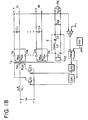
- Fig. 11 shows the embodiment when the present invention is applied to the current-type push-pull system.
- V o denotes the direct current power supply
- L4 denotes the choke coil for input
- N L1 denotes the primary coil of a choke coil L4
- N L2 denotes the secondary coil of a choke coil L4
- D3 denotes the diode connected with N L2 in series
- Q1 and Q2 denote the switching transistors
- D4 denotes the diode provided between collector and emitter of the transistor Q1
- D5 denotes the diode provided between collector and emitter of the transistor Q2
- T3 denotes the inverter trans
- N p1 and N p2 denote the primary coils of T3
- N s5 and N s6 denote the secondary coils for direct current output which are magnetically combined with the primary coil N p1 and N p2
- N s2 denotes the secondary coil for alternating current output which is magnetically combined with the primary coils N p1 and N p2
- D1 and D2 denote rectification di
- A1 denotes the error amplification circuit which compares the direct current outputted by the secondary coils N s5 and N s6 with the standard voltage V R1 and outputs signals depending on the difference
- OsC denotes the oscillation circuit generating triangular waves
- PWM denotes the pulse modulation circuit to compare signals outputted by the error amplification circuit A1 with triangular waves outputted by the oscillation circuit OSC and to output a pulse whose width changes, depending on the movement of cross-point
- D R1 and D R2 denote the drive circuits which amplify the pulse and add to the base of transistors Q1 and Q2.
- the direct voltage V1 is stabilized by controlling the duty factor or transistors Q1 and Q2.
- the choke coil L4 operates to control the current so that the input current can be constant.
- the energy is accumulated in the choke coil L4.
- the energy accumulated in the choke coil L4 is returned to the input electric power V o through an energy return coil N L2 when the transistors Q1 and Q2 are OFF.
- the voltage loaded with the primary coil becomes constant, the voltage is induced with each secondary coil and the direct current output voltage is generated in proportion to its turn ratio.
- the direct output voltage is stabilized by controlling the duty factor of the transistors Q1 and Q2.
- the product of the voltage generated with the secondary coil N s5 and N s6 and ON-time of the transistors Q1 and Q2 is controlled to be constant without regard to the change in the input voltage and load.
- the required current can be supplied to the alternating load Rl with the adequate selection of the choke coil L2 and the capacitor C3 without influencing the change of input voltage and load.
- Fig. 12 shows the embodiment when the present invention is applied to the converter of current type 1-transistor system.
- L4 is a choke coil disposed at the input side and others are similar to Fig. 11.
- the transformer T3 excited by the coil N p1 are magnetized from zero to one side only on a B-H curve. This point is different from that in Fig. 11 using two switching transistors.
- the exciting energy of the transformer T3 is transferred to the load channel V1 through a diode D2 as the other half-wave of the alternating output current.
- the alternating current voltage waveform is generated with the alternating current load Rl by the coil N s2 .
- the voltage waveform of the coil N s2 is expressed by the following formula, corresponding to the positive and negative half-waves; (N s2 /N s5 )V1, (N s2 /N p2 )V1
- the energy of the transformer T3 supplied from the alternating current coil N s2 to the alternating current load RL is entirely the exciting energy.
- the transformer T3 is required to have the exciting energy to maintain the power supply of a half-wave of the alternating current load by providing an air gap on the magnetic path.
- emission of the exciting energy of the T3 is carried out by the coil N s6 .
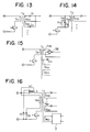
- Fig. 14 shows the example that partial exciting energy of transformer T3 can be absorbed by a voltage clamp circuit comprising a diode D5, a condenser C5 and a resistor R5.
- the back-electromotive force of the coil N p can be (N p /N s5 )V1, due to adequate selection of each constant of the condenser C5 and the resistor R5.
- the alternating current voltage waveform whose positive and negative amplitudes are equal is generated in the coil N s2 .
- Fig. 15 shows another process for consuming the energy of the transformer T3 through the coil N s5 .
- the coil voltage can be led to the output side during either the ON or OFF period by installing a diode bridge DB with the coil N s5 in series.
- the diode bridge can supply both positive and negative half-waves of the induction voltage of the coil N s5 are clamped with the output voltage V1.
- Fig. 16 shows the system for returning the partial exciting energy from the transformer to the input.
- N p2 is a return coil which returns exciting engergy to the input through a diode D5.
- the positive amplitude of the alternating current inducted with the coil N s2 is not equal to the negative one.
- the product of the positive voltage-time is equal to that of the negative voltage-time and electric power can be loaded with the alternating current load Rl, while the energy of the positive and negative voltages are maintained to be equal.
- the energy of the choke coil L4 is supplied to the direct current output V1 when transistors Q1 and Q2 are OFF.
- a return coil is not provided in the choke coil L4.
- the transistors Q1 and Q2 are necessarily driven so that its duty factor can be 50% ⁇ 100%.
- the energy of the choke coil L4 is added to the input energy and converted to the second coil side after being loaded with the first coil.
- the resonance circuit composed of the choke coil L2 and the capacitor C3 is used as a serial impedance circuit Z for the alternating current load.
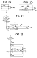
- impedance is required only its existence for the negative resistance property of alternating load, only one choke coil L2 may be used as shown in Fig. 19.
- the load current does not become a sine wave when only using choke coil L2. And also it is possible to use the choke coil L2 shown in Fig. 19 in the place of condenser for the negative resistance property of alternating load.
- the choke coil L2 is operated as an impedance to control the current
- the capacitor C3 and the choke coil L3 are forming a parallel resonance circuit.
- the sine wave current can be supplied to the alternating current load Rl by setting the resonance frequency of the parallel resonance circuit to the switching frequency.
- the choke coil can be used in place of condenser.
- the relay joint for lighting the fluorescent lamp has been connected with the alternating current load Rl in parallel, it can also be connected in series as shown in Fig. 21.
- a relay contact K a is opened while the fluorescent lamp is not lit.
- the relay contact K a is closed.
- the current supplied to the fluorescent lamp is 0 and the voltage E2 of the coil N s2 is entirely loaded to the fluorescent lamp.
- the fluorescent lamp starts for discharge because its voltage is higher than that at the start of discharge. Then, the current is supplied to the fluorescent lamp and the voltage E2 is reduced by the impedance Z, therefore, the required voltage for lighting can be loaded with the fluorescent lamp when the values of the choke coil L2 and the capacitor C3 are determined in advance.
- the required heater voltage for a heater of a fluorescent lamp FL is supplied from the coils of two heaters which are N s3 and N s4 of a transformer.
- the heater coil is required to have only one or two turns, and voltage becomes several volts per turn.
- the setting of the coil at a unit of an integer may change the generating voltage substantially.
- condensers C H1 and C C2 are connected with heaters in series as impedances so that the heater voltage can be set to the required value.
- the impedance circuit connected to the secondary coils of the transformer for creating alternating power due to the provision of the impedance circuit connected to the secondary coils of the transformer for creating alternating power, variations in voltage applied to an alternating current load can be absorbed by the impedance of the impedance circuit even through the above-mentioned alternating current load has a negative resistance characteristic.
- the impedance circuit connected to the secondary circuit for alternating current power is used as a resonance circuit, and the switching frequency of the switching transistor is shifted from the resonance frequency of the resonance circuit so that the the resonance circuit has a certain impedance, the output alternating current can be stabilized, and can have a substantially sinusoidal waveform.
- the aforementioned impedance circuit is composed of an resonance circuit and a coil or a capacitor, and the switching frequency of the switching transistor is adjusted to the resonance frequency of the resonance circuit, alternating current output can be made to be stabilized sinusoidal electrical current.
Landscapes
- Engineering & Computer Science (AREA)
- Power Engineering (AREA)
- Dc-Dc Converters (AREA)
- Inverter Devices (AREA)
Applications Claiming Priority (2)
| Application Number | Priority Date | Filing Date | Title |
|---|---|---|---|
| JP73423/86 | 1986-03-31 | ||
| JP61073423A JPS62233067A (ja) | 1986-03-31 | 1986-03-31 | 安定化電源装置 |
Publications (3)
| Publication Number | Publication Date |
|---|---|
| EP0240312A2 EP0240312A2 (en) | 1987-10-07 |
| EP0240312A3 EP0240312A3 (en) | 1989-07-26 |
| EP0240312B1 true EP0240312B1 (en) | 1993-03-24 |
Family
ID=13517800
Family Applications (1)
| Application Number | Title | Priority Date | Filing Date |
|---|---|---|---|
| EP87302791A Expired - Lifetime EP0240312B1 (en) | 1986-03-31 | 1987-03-31 | Stabilized electric power apparatus for generating direct and alternating current simultaneously in one transformer |
Country Status (5)
| Country | Link |
|---|---|
| US (1) | US4881014A (ko) |
| EP (1) | EP0240312B1 (ko) |
| JP (1) | JPS62233067A (ko) |
| KR (1) | KR870009529A (ko) |
| DE (1) | DE3784956T2 (ko) |
Families Citing this family (30)
| Publication number | Priority date | Publication date | Assignee | Title |
|---|---|---|---|---|
| JP2643163B2 (ja) * | 1987-08-13 | 1997-08-20 | キヤノン株式会社 | 電源装置 |
| DE3742921A1 (de) * | 1987-12-17 | 1989-06-29 | Pintsch Bamag Ag | Vorschaltgeraet fuer eine entladungslampe |
| CA1304448C (en) * | 1988-01-19 | 1992-06-30 | Cecil Winston Deisch | Power factor improving arrangement |
| US4924369A (en) * | 1988-01-26 | 1990-05-08 | Siemens Aktiengesellschaft | Regulated blocking converter wherein switch conduction time increases with higher output voltages |
| US5023518A (en) * | 1988-12-12 | 1991-06-11 | Joseph A. Urda | Ballast circuit for gaseous discharge lamp |
| US5282122A (en) * | 1992-08-03 | 1994-01-25 | Modular Devices, Inc. | High voltage power supply topology suited for miniaturization |
| JPH08154378A (ja) * | 1994-09-30 | 1996-06-11 | Sony Corp | スイッチング電源回路 |
| KR0119883B1 (ko) * | 1994-12-22 | 1997-10-30 | 김광호 | 스위칭 전원장치용 컨트롤러 및 이를 이용한 스위칭 전원장치 |
| US5654880A (en) * | 1996-01-16 | 1997-08-05 | California Institute Of Technology | Single-stage AC-to-DC full-bridge converter with magnetic amplifiers for input current shaping independent of output voltage regulation |
| DE19609123C2 (de) * | 1996-03-08 | 1998-01-29 | Siemens Ag | Schaltungsanordnung für Schaltnetzteile mit mehreren lastunabhängigen Ausgangsspannungen |
| TW349287B (en) * | 1996-09-12 | 1999-01-01 | Thomson Consumer Electronics | A forward converter with an inductor coupled to a transformer winding |
| US7269034B2 (en) | 1997-01-24 | 2007-09-11 | Synqor, Inc. | High efficiency power converter |
| US6049471A (en) * | 1998-02-11 | 2000-04-11 | Powerdsine Ltd. | Controller for pulse width modulation circuit using AC sine wave from DC input signal |
| US5828558A (en) * | 1998-02-11 | 1998-10-27 | Powerdsine, Ltd. | PWN controller use with open loop flyback type DC to AC converter |
| US6252787B1 (en) * | 2000-05-12 | 2001-06-26 | Honeywell International Inc. | Controllable circuit for providing bi-directional current to a load |
| US6483726B2 (en) * | 2001-03-02 | 2002-11-19 | Delta Electronics, Inc. | Auxiliary output voltage control circuit of flyback power converter with a magnetic amplifier |
| EP1384393A1 (en) * | 2001-04-20 | 2004-01-28 | Koninklijke Philips Electronics N.V. | Circuit arrangement for discharge lamp comprising a resonant half-bridge converter driven by a class-e driver |
| US7821684B2 (en) * | 2002-04-23 | 2010-10-26 | Chen-Hsiang Shih | Circuit module integrating a light driver and an optical |
| US7994734B2 (en) * | 2006-12-13 | 2011-08-09 | Osram Gesellschaft mit beschränkter Haftung | Circuit arrangement for operation of discharge lamps, and method for operation of discharge lamps |
| KR20100014323A (ko) * | 2006-12-21 | 2010-02-10 | 오스람 게젤샤프트 미트 베쉬랭크터 하프퉁 | 광원들과 같은 전기적 부하들을 급전하기 위한 셀 어레인지먼트, 그에 대응하는 회로 및 설계 방법 |
| JP2008234965A (ja) * | 2007-03-20 | 2008-10-02 | Sanken Electric Co Ltd | 放電管点灯装置及び半導体集積回路 |
| JP4277127B2 (ja) * | 2007-08-22 | 2009-06-10 | サンケン電気株式会社 | 交流電源装置 |
| US8872439B2 (en) * | 2010-04-30 | 2014-10-28 | Texas Instruments Incorporated | System and methods for providing equal currents to current driven loads |
| JP2013026911A (ja) * | 2011-07-22 | 2013-02-04 | Nec Access Technica Ltd | 電圧生成装置および電圧生成方法 |
| US10199950B1 (en) | 2013-07-02 | 2019-02-05 | Vlt, Inc. | Power distribution architecture with series-connected bus converter |
| US20160322915A1 (en) * | 2015-04-28 | 2016-11-03 | University Of Connecticut | Dual AC and DC Output Flyback Converter and Associated Systems and Methods |
| JP6565788B2 (ja) * | 2016-05-13 | 2019-08-28 | 株式会社デンソー | 電力変換システム |
| KR20210040724A (ko) * | 2019-10-04 | 2021-04-14 | 주식회사 엘지화학 | 배터리 관리 장치 |
| DE102021200582A1 (de) | 2021-01-22 | 2022-07-28 | Vitesco Technologies GmbH | Galvanisch trennender Bordnetz-Gleichspannungswandler, Fahrzeugbordnetz mit Bordnetz-Gleichspannungswandler und Verfahren zum Betreiben eines galvanisch trennenden Gleichspannungswandlers |
| US11991806B2 (en) * | 2021-07-30 | 2024-05-21 | Shenzhen Billda Technology Co., Ltd | Emergency output circuit for starting LED lamp tubes with leakage protection |
Family Cites Families (13)
| Publication number | Priority date | Publication date | Assignee | Title |
|---|---|---|---|---|
| US3170085A (en) * | 1961-04-19 | 1965-02-16 | Gen Electric | Ballast circuit and system for dimming gaseous discharge lamps |
| DE2919905C2 (de) * | 1979-05-17 | 1982-08-19 | Standard Elektrik Lorenz Ag, 7000 Stuttgart | Schaltnetzteil nach dem Sperrwandler- oder Flußwandlerprinzip |
| DE3008887C2 (de) * | 1980-03-07 | 1982-06-24 | Siemens AG, 1000 Berlin und 8000 München | Gegentaktumrichter mit einem sättigbaren Übertrager |
| DE3036616A1 (de) * | 1980-09-29 | 1982-04-22 | Siemens AG, 1000 Berlin und 8000 München | Anordnung mit einer regeleinrichtung mit einem geregelten kreis und einem damit gekoppelten weiteren kreis |
| US4392087A (en) * | 1980-11-26 | 1983-07-05 | Honeywell, Inc. | Two-wire electronic dimming ballast for gaseous discharge lamps |
| US4451876A (en) * | 1981-06-19 | 1984-05-29 | Hitachi Metals, Ltd. | Switching regulator |
| AU555174B2 (en) * | 1981-09-18 | 1986-09-18 | Oy Helvar | Electronic ballast for a discharge lamp |
| DE3140175A1 (de) * | 1981-10-08 | 1983-04-28 | Licentia Gmbh | Transistorvorschalt-geraet |
| NL8105160A (nl) * | 1981-11-16 | 1983-06-16 | Philips Nv | Schakeling voor het omzetten van een ingangsgelijkspanning in een uitgangsgelijkspanning. |
| US4415839A (en) * | 1981-11-23 | 1983-11-15 | Lesea Ronald A | Electronic ballast for gaseous discharge lamps |
| US4535399A (en) * | 1983-06-03 | 1985-08-13 | National Semiconductor Corporation | Regulated switched power circuit with resonant load |
| US4687971A (en) * | 1984-11-08 | 1987-08-18 | Fuji Xerox Company, Limited | Power supply for discharge lamp |
| DE3588108T2 (de) * | 1984-12-28 | 1996-11-07 | Toshiba Kawasaki Kk | Stabilisierende Leistungsquellenvorrichtung |
-
1986
- 1986-03-31 JP JP61073423A patent/JPS62233067A/ja active Pending
-
1987
- 1987-03-31 EP EP87302791A patent/EP0240312B1/en not_active Expired - Lifetime
- 1987-03-31 DE DE8787302791T patent/DE3784956T2/de not_active Expired - Fee Related
- 1987-03-31 KR KR870002994A patent/KR870009529A/ko not_active Application Discontinuation
-
1988
- 1988-12-20 US US07/287,632 patent/US4881014A/en not_active Expired - Fee Related
Also Published As
| Publication number | Publication date |
|---|---|
| DE3784956D1 (de) | 1993-04-29 |
| JPS62233067A (ja) | 1987-10-13 |
| EP0240312A2 (en) | 1987-10-07 |
| KR870009529A (ko) | 1987-10-27 |
| EP0240312A3 (en) | 1989-07-26 |
| US4881014A (en) | 1989-11-14 |
| DE3784956T2 (de) | 1993-07-01 |
Similar Documents
| Publication | Publication Date | Title |
|---|---|---|
| EP0240312B1 (en) | Stabilized electric power apparatus for generating direct and alternating current simultaneously in one transformer | |
| US4980811A (en) | Power source apparatus | |
| US4677534A (en) | Stabilizing power source apparatus | |
| US6013969A (en) | Piezoelectric transformer inverter | |
| US6654259B2 (en) | Resonance type switching power supply unit | |
| US6307761B1 (en) | Single stage high power-factor converter | |
| EP0837546B1 (en) | Power circuit | |
| JP2010503375A (ja) | 変換回路を制御する適合回路 | |
| US5835368A (en) | Power-factor improvement converter | |
| JPH0626469B2 (ja) | マグネトロン駆動装置 | |
| JP2000032750A (ja) | Ac/dcコンバ―タ | |
| EP0725475B1 (en) | DC converter with improved power factor | |
| US5946201A (en) | Boost-up power factor correcting circuit using a power feedback | |
| JPH08130873A (ja) | 電流共振型スイッチング電源回路 | |
| JPH06327247A (ja) | 高力率電源供給装置 | |
| EP0477587A1 (en) | Power apparatus | |
| JPH05207738A (ja) | マグネトロン駆動用電源装置 | |
| JP2643163B2 (ja) | 電源装置 | |
| JP2000116154A (ja) | 2重共振回路により電源を得る方法およびその装置 | |
| JPH034492A (ja) | 放電ランプ用安定回路 | |
| JP2001273996A (ja) | 放電灯点灯装置及び該放電灯点灯装置を備えた画像処理装置 | |
| JPH0528716Y2 (ko) | ||
| JPS59186297A (ja) | スイツチング電源 | |
| JPH09247941A (ja) | スイッチング電源装置 | |
| KR900011129Y1 (ko) | 전자식 트랜스포머의 고역율 정류회로 |
Legal Events
| Date | Code | Title | Description |
|---|---|---|---|
| PUAI | Public reference made under article 153(3) epc to a published international application that has entered the european phase |
Free format text: ORIGINAL CODE: 0009012 |
|
| 17P | Request for examination filed |
Effective date: 19870410 |
|
| AK | Designated contracting states |
Kind code of ref document: A2 Designated state(s): DE IT NL |
|
| PUAL | Search report despatched |
Free format text: ORIGINAL CODE: 0009013 |
|
| AK | Designated contracting states |
Kind code of ref document: A3 Designated state(s): DE IT NL |
|
| 17Q | First examination report despatched |
Effective date: 19910508 |
|
| GRAA | (expected) grant |
Free format text: ORIGINAL CODE: 0009210 |
|
| AK | Designated contracting states |
Kind code of ref document: B1 Designated state(s): DE IT NL |
|
| REF | Corresponds to: |
Ref document number: 3784956 Country of ref document: DE Date of ref document: 19930429 |
|
| ITF | It: translation for a ep patent filed |
Owner name: BUGNION S.P.A. |
|
| PLBE | No opposition filed within time limit |
Free format text: ORIGINAL CODE: 0009261 |
|
| STAA | Information on the status of an ep patent application or granted ep patent |
Free format text: STATUS: NO OPPOSITION FILED WITHIN TIME LIMIT |
|
| 26N | No opposition filed | ||
| PGFP | Annual fee paid to national office [announced via postgrant information from national office to epo] |
Ref country code: NL Payment date: 19970327 Year of fee payment: 11 |
|
| PGFP | Annual fee paid to national office [announced via postgrant information from national office to epo] |
Ref country code: DE Payment date: 19970404 Year of fee payment: 11 |
|
| PG25 | Lapsed in a contracting state [announced via postgrant information from national office to epo] |
Ref country code: NL Free format text: LAPSE BECAUSE OF NON-PAYMENT OF DUE FEES Effective date: 19981001 |
|
| NLV4 | Nl: lapsed or anulled due to non-payment of the annual fee |
Effective date: 19981001 |
|
| PG25 | Lapsed in a contracting state [announced via postgrant information from national office to epo] |
Ref country code: DE Free format text: LAPSE BECAUSE OF NON-PAYMENT OF DUE FEES Effective date: 19981201 |
|
| PG25 | Lapsed in a contracting state [announced via postgrant information from national office to epo] |
Ref country code: IT Free format text: LAPSE BECAUSE OF NON-PAYMENT OF DUE FEES;WARNING: LAPSES OF ITALIAN PATENTS WITH EFFECTIVE DATE BEFORE 2007 MAY HAVE OCCURRED AT ANY TIME BEFORE 2007. THE CORRECT EFFECTIVE DATE MAY BE DIFFERENT FROM THE ONE RECORDED. Effective date: 20050331 |