EP0240293A2 - Frequenzstabilisierte Lichtquelle - Google Patents
Frequenzstabilisierte Lichtquelle Download PDFInfo
- Publication number
- EP0240293A2 EP0240293A2 EP87302752A EP87302752A EP0240293A2 EP 0240293 A2 EP0240293 A2 EP 0240293A2 EP 87302752 A EP87302752 A EP 87302752A EP 87302752 A EP87302752 A EP 87302752A EP 0240293 A2 EP0240293 A2 EP 0240293A2
- Authority
- EP
- European Patent Office
- Prior art keywords
- diffraction grating
- semiconductor laser
- light source
- laser element
- corrugated
- Prior art date
- Legal status (The legal status is an assumption and is not a legal conclusion. Google has not performed a legal analysis and makes no representation as to the accuracy of the status listed.)
- Granted
Links
Images


Classifications
-
- G—PHYSICS
- G02—OPTICS
- G02B—OPTICAL ELEMENTS, SYSTEMS OR APPARATUS
- G02B27/00—Optical systems or apparatus not provided for by any of the groups G02B1/00 - G02B26/00, G02B30/00
-
- H—ELECTRICITY
- H01—ELECTRIC ELEMENTS
- H01S—DEVICES USING THE PROCESS OF LIGHT AMPLIFICATION BY STIMULATED EMISSION OF RADIATION [LASER] TO AMPLIFY OR GENERATE LIGHT; DEVICES USING STIMULATED EMISSION OF ELECTROMAGNETIC RADIATION IN WAVE RANGES OTHER THAN OPTICAL
- H01S5/00—Semiconductor lasers
- H01S5/10—Construction or shape of the optical resonator, e.g. extended or external cavity, coupled cavities, bent-guide, varying width, thickness or composition of the active region
- H01S5/14—External cavity lasers
- H01S5/141—External cavity lasers using a wavelength selective device, e.g. a grating or etalon
-
- G—PHYSICS
- G02—OPTICS
- G02B—OPTICAL ELEMENTS, SYSTEMS OR APPARATUS
- G02B5/00—Optical elements other than lenses
- G02B5/18—Diffraction gratings
- G02B5/1809—Diffraction gratings with pitch less than or comparable to the wavelength
-
- H—ELECTRICITY
- H01—ELECTRIC ELEMENTS
- H01S—DEVICES USING THE PROCESS OF LIGHT AMPLIFICATION BY STIMULATED EMISSION OF RADIATION [LASER] TO AMPLIFY OR GENERATE LIGHT; DEVICES USING STIMULATED EMISSION OF ELECTROMAGNETIC RADIATION IN WAVE RANGES OTHER THAN OPTICAL
- H01S3/00—Lasers, i.e. devices using stimulated emission of electromagnetic radiation in the infrared, visible or ultraviolet wave range
- H01S3/05—Construction or shape of optical resonators; Accommodation of active medium therein; Shape of active medium
- H01S3/08—Construction or shape of optical resonators or components thereof
-
- H—ELECTRICITY
- H01—ELECTRIC ELEMENTS
- H01S—DEVICES USING THE PROCESS OF LIGHT AMPLIFICATION BY STIMULATED EMISSION OF RADIATION [LASER] TO AMPLIFY OR GENERATE LIGHT; DEVICES USING STIMULATED EMISSION OF ELECTROMAGNETIC RADIATION IN WAVE RANGES OTHER THAN OPTICAL
- H01S3/00—Lasers, i.e. devices using stimulated emission of electromagnetic radiation in the infrared, visible or ultraviolet wave range
- H01S3/10—Controlling the intensity, frequency, phase, polarisation or direction of the emitted radiation, e.g. switching, gating, modulating or demodulating
- H01S3/105—Controlling the intensity, frequency, phase, polarisation or direction of the emitted radiation, e.g. switching, gating, modulating or demodulating by controlling the mutual position or the reflecting properties of the reflectors of the cavity, e.g. by controlling the cavity length
- H01S3/1055—Controlling the intensity, frequency, phase, polarisation or direction of the emitted radiation, e.g. switching, gating, modulating or demodulating by controlling the mutual position or the reflecting properties of the reflectors of the cavity, e.g. by controlling the cavity length one of the reflectors being constituted by a diffraction grating
Definitions
- the present invention relates to a light source for use in optical communication, optical recording and optical measurement.
- semiconductor laser has been used as a light source for optical communications and optical recording systems.
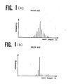
- semiconductor laser since semiconductor laser has its oscillation wavelength varied depending on the temperature and the amount of injection current, it oscillates in multiple modes as shown in Fig. l(a).
- the laser chip is combined with a frequency selective external cavity so as to construct a light source which is controlled to oscillate at a specific wavelength as shown in Fig. l(b).
- an echellette grating having a saw tooth cross-section, has been used for the external cavity.
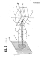
- Fig. 2 shows the structure of the conventional light source.
- a light beam l9 coming out of one facet of a semiconductor laser chip l is collimated by a lens 2, and it is incident on an echellette grating l2.
- the incident light l9 is dispersed depending on its wavelengths, and a light beam l6 with a specific wavelength determined from the angle of the grating l2 is fed back to the active layer l3 of the semiconductor laser chip l.
- the semiconductor laser chip l oscillates at the wavelength of the feedback light l6 and emits an output light beam 20 with a stabilized frequency from the other facet.
- the oscillation frequency of the semiconductor laser chip l can be changed by rotating the echellette grating l2.
- the conventional frequency stabilized light source has been restricted in the disposition of the semiconductor laser chip l and grating l2.
- the echellette grating l2 has a higher diffraction efficiency for the polarized light which electric field is perpendicular to the groove direction N, i.e., S-polarization, while it has a lower diffraction efficiency for the polarized light which electric field is parallel to the groove direction N, i.e., P-polarization.
- the semiconductor laser chip l has the output light l9 polarized in the Y direction parallel to its pn junction plane, and therefore the components must have been disposed such that the pn junction plane l4 of the semiconductor laser chip l is at right angles with the groove direction N of the echellette grating l2.
- feedback light beams l5 and l6 from the grating l2 align along the pn junction plane l4, causing the light beams l5 of unnecessary adjacent mode to be incident on the active layer l3 as shown in Fig. 3.
- the frequency stabilized light source of the invention comprises a semiconductor laser chip and a finite Fourier diffraction grating with a corrugation having continuous first-order differential coefficients.
- the semiconductor laser chip emits a light beam from its one facet to the finite Fourier diffraction grating, and a diffracted light beam from the grating is fed back to the semiconductor laser chip, so that an output light beam having a stable wavelength is obtained at the other facet of the laser chip.
- the components are disposed so that the pn junction plane of the semiconductor laser chip is substantially parallel to the groove direction of the finite Foruier diffraction grating.
- the first embodiment shown in Fig. 4 includes a semiconductor laser chip l, a lens 2, a finite Fourier diffraction grating 3 and an anti-reflection coating 5.
- a light beam l9 coming out of one facet of the semiconductor laser chip l is collimated by the lens 2, and it is incident on the finite Fourier grating 3.
- the incident light is dispersed depending on its wavelengths, and the light with a specific wavelength determined from the angle of the grating 3 is fed back to the active layer l3 of the semiconductor laser chip l.
- the semiconductor laser chip l oscillates stably at the wavelength of the feedback light l6, and emits a frequency stabilized output light 20 from the other facet thereof.
- the output light 20 from the semiconductor laser chip l has its wavelength varied by the rotation of the grating 3.
- the anti-reflection coating 5 is to enhance the coupling efficiency of the semiconductor laser chip l with the feedback light l6 from the grating 3.
- the embodiment of Fig. 4 has the orthogonal relationship between the dispersing direction X of the grating 3 and the direction Y of the pn junction plane of the laser chip l.
- the finite Fourier grating 3 has its cross-section shaped smoothly due to the absence of discontinuous points in the first order differential coefficients, as shown in Figs. 5(a), 5(b) and 5(c), and it can be expressed by the fundamental sinusoidal wave superimposed by its finite harmonics.
- the profile of Fig. 5(a) is symmetric with respect to the ridge center, while the profile shown in Fig. 5(b) is asymmetric, and their difference is derived from the phase difference of the harmonic components.
- the profile of Fig. 5(c) is of the case of a sole fundamental sinusoidal wave.
- the finite Fourier grating features the high efficiency of polarization characteristic which cannot be achieved by the echellette grating.
- Fig. 6 shows the measurement result of diffraction efficiency for the polarized light by the conventional echellette grating and the finite Fourier grating.
- the diffraction efficiencies of the both cases are plotted on the vertical axis against the angle ⁇ between the dispersing direction X of the grating and the direction Y of the pn junction plane on the horizontal axis, using a measurement wavelength ⁇ of 0.83 ⁇ m and a grating groove pitch of 0.83 ⁇ m.
- the finite Fourier grating has less polarization dependency and higher efficiency. Its efficiency is higher by 40% than that of the echellette grating in P-polarization.
- the finite Fourier grating has especially high efficiency when the light wavelength ⁇ and the grating groove pitch d are related as: 0.2 ⁇ ⁇ /d ⁇ l.7.
- the efficiency characteristic can be changed by choosing the value of the parameter ⁇ /d. Accordingly, it is not necessary to confine the light incident system to the S-polarized light.
- the spurious lights l5 do not contribute to the oscillation of the semiconductor laser chip l so far as the equation (l) is met.
- the orthogonal arrangement of the grating dispersing direction X and the pn junction plane Y provides the best isolation of the spurious light spots l5 as shown in Fig. 8(b), and this is the case of the highest wavelength adjustment accuracy.
- Fig. 9 shows the oscillating spectrum of the frequency stabilized light source of the invention. Adjoining spurious modes are completely suppressed, and the laser oscillates at a sole wavelength. Due to P-polarization, the finite Fourier grating 3 provides a high diffraction light intensity, and therefore the effect of optical feedback is high, the wavelength tunable range is wide, and the output light 20 is strong. In case the oscillation is exerted in the vicinity of the gain center of the semiconductor laser chip l, the anti-reflection coating 5 is not always necessary.
- a sinusoidal-corrugated diffraction grating shown in Fig. 5(c) is used as the finite Fourier grating 3, it can be manufactured easily and accurately by the holographical exposure method, and its smooth and symmetric profile makes replication easy for mass production. Therefore, this grating is advantageous in the cost reduction of the frequency stabilized light source.
- Fig. l0 shows the second embodiment of the present invention.
- the arrangement differs from the first embodiment in that a finite Fourier curvilinear-corrugated diffraction grating 9 is used as the finite Fourier grating 3.
- the finite Fourier curvilinear-corrugated grating 9 has its grooves curved in a zone- plate fashion, and it has a focusing function along with the dispersive function.
- the grating 9 by itself serves as a lens, eliminating the need of a collimating lens, and the simplified structure is suited to make the light source compact. Other features and effects are identical to the case of the first embodiment.
- Fig. ll shows the third embodiment of the present invention.
- the arrangement differs from the first embodiment in that a finite Fourier concave diffraction grating l0 is used as the finite Fourier grating 3.
- the finite Fourier concave grating l0 not only serves for dispersion, but being a concave mirror by itself it also works for focusing.
- Through the optimal selection for the curvature and grating parameters of the finite Fourier concave grating l0 outstanding focusing performance is exerted, and the elimination of lens is suited to make the light source compact.
- Other features and effects are identical to the case of the first embodiment.
Landscapes
- Physics & Mathematics (AREA)
- Electromagnetism (AREA)
- Optics & Photonics (AREA)
- General Physics & Mathematics (AREA)
- Engineering & Computer Science (AREA)
- Plasma & Fusion (AREA)
- Condensed Matter Physics & Semiconductors (AREA)
- Semiconductor Lasers (AREA)
- Diffracting Gratings Or Hologram Optical Elements (AREA)
Applications Claiming Priority (4)
| Application Number | Priority Date | Filing Date | Title |
|---|---|---|---|
| JP61073503A JPS62230074A (ja) | 1986-03-31 | 1986-03-31 | 周波数安定化光源 |
| JP73503/86 | 1986-03-31 | ||
| JP257233/86 | 1986-10-29 | ||
| JP25723386A JPH0722217B2 (ja) | 1986-10-29 | 1986-10-29 | 周波数安定化光源 |
Publications (3)
| Publication Number | Publication Date |
|---|---|
| EP0240293A2 true EP0240293A2 (de) | 1987-10-07 |
| EP0240293A3 EP0240293A3 (en) | 1988-09-14 |
| EP0240293B1 EP0240293B1 (de) | 1992-10-28 |
Family
ID=26414648
Family Applications (1)
| Application Number | Title | Priority Date | Filing Date |
|---|---|---|---|
| EP87302752A Expired - Lifetime EP0240293B1 (de) | 1986-03-31 | 1987-03-30 | Frequenzstabilisierte Lichtquelle |
Country Status (4)
| Country | Link |
|---|---|
| US (1) | US4913525A (de) |
| EP (1) | EP0240293B1 (de) |
| KR (1) | KR910000827B1 (de) |
| DE (1) | DE3782355T2 (de) |
Cited By (2)
| Publication number | Priority date | Publication date | Assignee | Title |
|---|---|---|---|---|
| FR2647974A1 (fr) * | 1989-05-31 | 1990-12-07 | Jenoptik Jena Gmbh | Dispositif pour le retrocouplage du rayonnement d'une diode a effet laser |
| DE102004016638A1 (de) * | 2004-03-30 | 2005-10-20 | Zeiss Carl | Beugungsgitter, insbesondere Reflexionsgitter |
Families Citing this family (29)
| Publication number | Priority date | Publication date | Assignee | Title |
|---|---|---|---|---|
| DE3932097A1 (de) * | 1989-09-26 | 1991-04-04 | Max Planck Gesellschaft | Optischer pulskompressor |
| US5011264A (en) * | 1989-12-28 | 1991-04-30 | General Dynamics Corp., Electronics Divn. | Wide linear dynamic range optical modulator |
| US5222071A (en) * | 1991-02-21 | 1993-06-22 | Board Of Trustees Leland Stanford, Jr. University | Dynamic optical grating device |
| JP2755504B2 (ja) * | 1991-06-10 | 1998-05-20 | 松下電器産業株式会社 | 位相同期型半導体レーザ |
| US5386426A (en) * | 1992-09-10 | 1995-01-31 | Hughes Aircraft Company | Narrow bandwidth laser array system |
| US5351262A (en) * | 1992-09-10 | 1994-09-27 | Bell Communications Research, Inc. | Multi-stripe array grating integrated cavity laser |
| US5715092A (en) * | 1994-06-29 | 1998-02-03 | Eastman Kodak Company | Ferroelectric light frequency doubler device with a surface coating and having an inverted domain structure |
| US6370290B1 (en) * | 1997-09-19 | 2002-04-09 | Uniphase Corporation | Integrated wavelength-select transmitter |
| US6134253A (en) * | 1998-02-19 | 2000-10-17 | Jds Uniphase Corporation | Method and apparatus for monitoring and control of laser emission wavelength |
| US6289028B1 (en) | 1998-02-19 | 2001-09-11 | Uniphase Telecommunications Products, Inc. | Method and apparatus for monitoring and control of laser emission wavelength |
| US6560253B1 (en) | 1999-01-14 | 2003-05-06 | Jds Uniphase Corporation | Method and apparatus for monitoring and control of laser emission wavelength |
| US6456756B1 (en) | 1999-10-25 | 2002-09-24 | Aculight Corporation | Fiber raman amplifier pumped by an incoherently beam combined diode laser |
| US6538817B1 (en) | 1999-10-25 | 2003-03-25 | Aculight Corporation | Method and apparatus for optical coherence tomography with a multispectral laser source |
| US6501782B1 (en) | 1999-10-25 | 2002-12-31 | Aculight Corporation | Compact laser apparatus |
| US6529542B1 (en) | 2000-04-04 | 2003-03-04 | Aculight Corporation | Incoherent beam combined optical system utilizing a lens array |
| JP3849967B2 (ja) * | 2000-05-19 | 2006-11-22 | シャープ株式会社 | 光ピックアップ |
| US6587214B1 (en) | 2000-06-26 | 2003-07-01 | Jds Uniphase Corporation | Optical power and wavelength monitor |
| US6611341B2 (en) | 2000-10-10 | 2003-08-26 | Spectrasensors, Inc. | Method and system for locking transmission wavelengths for lasers in a dense wavelength division multiplexer utilizing a tunable etalon |
| US6671296B2 (en) * | 2000-10-10 | 2003-12-30 | Spectrasensors, Inc. | Wavelength locker on optical bench and method of manufacture |
| US6693928B2 (en) | 2000-10-10 | 2004-02-17 | Spectrasensors, Inc. | Technique for filtering chirp from optical signals |
| US6587484B1 (en) | 2000-10-10 | 2003-07-01 | Spectrasensor, Inc,. | Method and apparatus for determining transmission wavelengths for lasers in a dense wavelength division multiplexer |
| US6486950B1 (en) | 2000-12-05 | 2002-11-26 | Jds Uniphase Corporation | Multi-channel wavelength monitor |
| JP4085970B2 (ja) * | 2003-12-03 | 2008-05-14 | ソニー株式会社 | 外部共振器型半導体レーザ |
| JP2008529068A (ja) * | 2005-01-24 | 2008-07-31 | ソルラブス、 インコーポレイテッド | 高速に波長スキャンする小型マルチモードレーザ |
| RU2433516C2 (ru) * | 2009-11-27 | 2011-11-10 | Общество С Ограниченной Ответственностью "Новые Энергетические Технологии" | Способ синхронизации линейки лазерных диодов и фазовое решетчатое зеркало для его реализации |
| US8467430B2 (en) * | 2010-09-23 | 2013-06-18 | Daylight Solutions, Inc. | Continuous wavelength tunable laser source with optimum orientation of grating and gain medium |
| CN102280808A (zh) * | 2011-06-20 | 2011-12-14 | 青岛镭创光电技术有限公司 | 一种自倍频激光器 |
| TW201401699A (zh) * | 2012-04-09 | 2014-01-01 | Sony Corp | 半導體雷射裝置組立體 |
| JP7137321B2 (ja) * | 2018-02-28 | 2022-09-14 | 浜松ホトニクス株式会社 | 可動回折格子、外部共振器型レーザモジュール、可動回折格子の製造方法 |
Family Cites Families (2)
| Publication number | Priority date | Publication date | Assignee | Title |
|---|---|---|---|---|
| US4289371A (en) * | 1979-05-31 | 1981-09-15 | Xerox Corporation | Optical scanner using plane linear diffraction gratings on a rotating spinner |
| US4601036A (en) * | 1982-09-30 | 1986-07-15 | Honeywell Inc. | Rapidly tunable laser |
-
1987
- 1987-03-30 EP EP87302752A patent/EP0240293B1/de not_active Expired - Lifetime
- 1987-03-30 KR KR1019870002915A patent/KR910000827B1/ko not_active Expired
- 1987-03-30 DE DE8787302752T patent/DE3782355T2/de not_active Expired - Fee Related
-
1989
- 1989-04-03 US US07/334,793 patent/US4913525A/en not_active Expired - Lifetime
Cited By (2)
| Publication number | Priority date | Publication date | Assignee | Title |
|---|---|---|---|---|
| FR2647974A1 (fr) * | 1989-05-31 | 1990-12-07 | Jenoptik Jena Gmbh | Dispositif pour le retrocouplage du rayonnement d'une diode a effet laser |
| DE102004016638A1 (de) * | 2004-03-30 | 2005-10-20 | Zeiss Carl | Beugungsgitter, insbesondere Reflexionsgitter |
Also Published As
| Publication number | Publication date |
|---|---|
| DE3782355T2 (de) | 1993-04-01 |
| KR870009248A (ko) | 1987-10-24 |
| US4913525A (en) | 1990-04-03 |
| EP0240293A3 (en) | 1988-09-14 |
| KR910000827B1 (ko) | 1991-02-09 |
| DE3782355D1 (de) | 1992-12-03 |
| EP0240293B1 (de) | 1992-10-28 |
Similar Documents
| Publication | Publication Date | Title |
|---|---|---|
| US4913525A (en) | Frequency stabilized light source | |
| US5555253A (en) | Technique for locking a laser diode to a passive cavity | |
| US7394842B2 (en) | Volume bragg lasers based on high efficiency diffractive elements in photo-thermo-refractive glass | |
| EP2521226B1 (de) | Laser mit externem resonator | |
| Oka et al. | Laser-diode-pumped phase-locked Nd: YAG laser arrays | |
| US7822096B2 (en) | Alignment and wavelength selection in external cavity lasers | |
| JPH0766482A (ja) | 可変波長光源 | |
| US7609743B2 (en) | Volume Bragg lasers based on high efficiency diffractive elements in photo-thermo-refractive glass | |
| Pillai et al. | Paraxial-misalignment insensitive external-cavity semiconductor-laser array emitting near-diffraction limited single-lobed beam | |
| US6700904B2 (en) | Light source for an external cavity laser | |
| US20090022184A1 (en) | Wavelength tunable light source of external resonator type | |
| CN115117732A (zh) | 一种外腔可调谐半导体激光器 | |
| Hof et al. | Application of diode lasers as a spectroscopic tool at 670 nm | |
| US8681825B2 (en) | Grating external-cavity laser and quasi-synchronous tuning method thereof | |
| JPH05206579A (ja) | 外部共振器型レーザ装置 | |
| US20020163643A1 (en) | Optical interference apparatus and method | |
| JP3031976B2 (ja) | 半導体レーザ装置 | |
| JP2900703B2 (ja) | 狭帯域レーザ装置 | |
| Shine et al. | Tunable diode lasers | |
| JPH03145174A (ja) | 外部共振器型レーザ | |
| US7310183B1 (en) | Diffractive outcoupler for second harmonic generation | |
| US20110261843A1 (en) | Grating external-cavity semiconductor laser and quasi-synchronous tuning method thereof | |
| Akulshin et al. | Frequency chain towards the Ca intercombination line based on laser diodes: First step | |
| JPH0730183A (ja) | 半導体レーザー | |
| JPS62136890A (ja) | 半導体レ−ザ装置 |
Legal Events
| Date | Code | Title | Description |
|---|---|---|---|
| PUAI | Public reference made under article 153(3) epc to a published international application that has entered the european phase |
Free format text: ORIGINAL CODE: 0009012 |
|
| AK | Designated contracting states |
Kind code of ref document: A2 Designated state(s): DE FR GB NL |
|
| PUAL | Search report despatched |
Free format text: ORIGINAL CODE: 0009013 |
|
| AK | Designated contracting states |
Kind code of ref document: A3 Designated state(s): DE FR GB NL |
|
| 17P | Request for examination filed |
Effective date: 19890314 |
|
| 17Q | First examination report despatched |
Effective date: 19910423 |
|
| GRAA | (expected) grant |
Free format text: ORIGINAL CODE: 0009210 |
|
| AK | Designated contracting states |
Kind code of ref document: B1 Designated state(s): DE FR GB NL |
|
| REF | Corresponds to: |
Ref document number: 3782355 Country of ref document: DE Date of ref document: 19921203 |
|
| ET | Fr: translation filed | ||
| PLBE | No opposition filed within time limit |
Free format text: ORIGINAL CODE: 0009261 |
|
| STAA | Information on the status of an ep patent application or granted ep patent |
Free format text: STATUS: NO OPPOSITION FILED WITHIN TIME LIMIT |
|
| 26N | No opposition filed | ||
| PGFP | Annual fee paid to national office [announced via postgrant information from national office to epo] |
Ref country code: GB Payment date: 19970321 Year of fee payment: 11 |
|
| PGFP | Annual fee paid to national office [announced via postgrant information from national office to epo] |
Ref country code: DE Payment date: 19970404 Year of fee payment: 11 |
|
| PGFP | Annual fee paid to national office [announced via postgrant information from national office to epo] |
Ref country code: FR Payment date: 19980310 Year of fee payment: 12 |
|
| PGFP | Annual fee paid to national office [announced via postgrant information from national office to epo] |
Ref country code: NL Payment date: 19980326 Year of fee payment: 12 |
|
| PG25 | Lapsed in a contracting state [announced via postgrant information from national office to epo] |
Ref country code: GB Free format text: LAPSE BECAUSE OF NON-PAYMENT OF DUE FEES Effective date: 19980330 |
|
| GBPC | Gb: european patent ceased through non-payment of renewal fee |
Effective date: 19980330 |
|
| PG25 | Lapsed in a contracting state [announced via postgrant information from national office to epo] |
Ref country code: DE Free format text: LAPSE BECAUSE OF NON-PAYMENT OF DUE FEES Effective date: 19981201 |
|
| PG25 | Lapsed in a contracting state [announced via postgrant information from national office to epo] |
Ref country code: NL Free format text: LAPSE BECAUSE OF NON-PAYMENT OF DUE FEES Effective date: 19991001 |
|
| PG25 | Lapsed in a contracting state [announced via postgrant information from national office to epo] |
Ref country code: FR Free format text: LAPSE BECAUSE OF NON-PAYMENT OF DUE FEES Effective date: 19991130 |
|
| NLV4 | Nl: lapsed or anulled due to non-payment of the annual fee |
Effective date: 19991001 |
|
| REG | Reference to a national code |
Ref country code: FR Ref legal event code: ST |