EP0236807A2 - Objectif de spectromètre en technique de mesure par faisceau corpusculaire - Google Patents
Objectif de spectromètre en technique de mesure par faisceau corpusculaire Download PDFInfo
- Publication number
- EP0236807A2 EP0236807A2 EP87102318A EP87102318A EP0236807A2 EP 0236807 A2 EP0236807 A2 EP 0236807A2 EP 87102318 A EP87102318 A EP 87102318A EP 87102318 A EP87102318 A EP 87102318A EP 0236807 A2 EP0236807 A2 EP 0236807A2
- Authority
- EP
- European Patent Office
- Prior art keywords
- spectrometer
- deflection
- field
- optical axis
- objective
- Prior art date
- Legal status (The legal status is an assumption and is not a legal conclusion. Google has not performed a legal analysis and makes no representation as to the accuracy of the status listed.)
- Withdrawn
Links
- 238000000034 method Methods 0.000 title description 2
- 230000005291 magnetic effect Effects 0.000 claims abstract description 35
- 239000008186 active pharmaceutical agent Substances 0.000 claims abstract description 22
- 230000001960 triggered effect Effects 0.000 claims abstract description 6
- 239000013598 vector Substances 0.000 claims abstract description 6
- 238000005516 engineering process Methods 0.000 claims abstract description 3
- 230000003287 optical effect Effects 0.000 claims description 37
- 239000004020 conductor Substances 0.000 claims description 5
- 230000001133 acceleration Effects 0.000 claims description 3
- 238000004458 analytical method Methods 0.000 claims description 2
- 230000003595 spectral effect Effects 0.000 claims 1
- 239000000523 sample Substances 0.000 description 26
- 238000001514 detection method Methods 0.000 description 7
- 238000010894 electron beam technology Methods 0.000 description 7
- 230000005684 electric field Effects 0.000 description 6
- 238000005259 measurement Methods 0.000 description 5
- 229910000831 Steel Inorganic materials 0.000 description 3
- 239000013256 coordination polymer Substances 0.000 description 3
- 230000000694 effects Effects 0.000 description 3
- 239000012212 insulator Substances 0.000 description 3
- 239000010959 steel Substances 0.000 description 3
- 230000004075 alteration Effects 0.000 description 2
- 238000011161 development Methods 0.000 description 2
- 230000018109 developmental process Effects 0.000 description 2
- 239000002245 particle Substances 0.000 description 2
- 230000035945 sensitivity Effects 0.000 description 2
- 239000007787 solid Substances 0.000 description 2
- 238000004804 winding Methods 0.000 description 2
- 241000252095 Congridae Species 0.000 description 1
- 230000000712 assembly Effects 0.000 description 1
- 238000000429 assembly Methods 0.000 description 1
- 201000009310 astigmatism Diseases 0.000 description 1
- 239000003518 caustics Substances 0.000 description 1
- 238000010276 construction Methods 0.000 description 1
- 230000001419 dependent effect Effects 0.000 description 1
- 238000013461 design Methods 0.000 description 1
- 238000001493 electron microscopy Methods 0.000 description 1
- 238000010893 electron trap Methods 0.000 description 1
- 238000003384 imaging method Methods 0.000 description 1
- 230000001771 impaired effect Effects 0.000 description 1
- 230000003993 interaction Effects 0.000 description 1
- 238000011835 investigation Methods 0.000 description 1
- 239000002184 metal Substances 0.000 description 1
- 230000005855 radiation Effects 0.000 description 1
- 239000004065 semiconductor Substances 0.000 description 1
- 239000000126 substance Substances 0.000 description 1
- 238000012360 testing method Methods 0.000 description 1
- 230000036962 time dependent Effects 0.000 description 1
Images


Classifications
-
- G—PHYSICS
- G01—MEASURING; TESTING
- G01R—MEASURING ELECTRIC VARIABLES; MEASURING MAGNETIC VARIABLES
- G01R31/00—Arrangements for testing electric properties; Arrangements for locating electric faults; Arrangements for electrical testing characterised by what is being tested not provided for elsewhere
- G01R31/28—Testing of electronic circuits, e.g. by signal tracer
- G01R31/302—Contactless testing
- G01R31/305—Contactless testing using electron beams
-
- H—ELECTRICITY
- H01—ELECTRIC ELEMENTS
- H01J—ELECTRIC DISCHARGE TUBES OR DISCHARGE LAMPS
- H01J37/00—Discharge tubes with provision for introducing objects or material to be exposed to the discharge, e.g. for the purpose of examination or processing thereof
- H01J37/02—Details
- H01J37/04—Arrangements of electrodes and associated parts for generating or controlling the discharge, e.g. electron-optical arrangement or ion-optical arrangement
- H01J37/147—Arrangements for directing or deflecting the discharge along a desired path
- H01J37/1472—Deflecting along given lines
- H01J37/1474—Scanning means
-
- H—ELECTRICITY
- H01—ELECTRIC ELEMENTS
- H01J—ELECTRIC DISCHARGE TUBES OR DISCHARGE LAMPS
- H01J37/00—Discharge tubes with provision for introducing objects or material to be exposed to the discharge, e.g. for the purpose of examination or processing thereof
- H01J37/26—Electron or ion microscopes; Electron or ion diffraction tubes
- H01J37/266—Measurement of magnetic or electric fields in the object; Lorentzmicroscopy
- H01J37/268—Measurement of magnetic or electric fields in the object; Lorentzmicroscopy with scanning beams
-
- H—ELECTRICITY
- H01—ELECTRIC ELEMENTS
- H01J—ELECTRIC DISCHARGE TUBES OR DISCHARGE LAMPS
- H01J49/00—Particle spectrometers or separator tubes
- H01J49/44—Energy spectrometers, e.g. alpha-, beta-spectrometers
- H01J49/46—Static spectrometers
- H01J49/48—Static spectrometers using electrostatic analysers, e.g. cylindrical sector, Wien filter
- H01J49/488—Static spectrometers using electrostatic analysers, e.g. cylindrical sector, Wien filter with retarding grids
Definitions
- the invention relates to a spectrometer objective for the Korpuskuiarstrahi measuring technique according to the preamble of claim 1.
- This arrangement is a magnetic objective lens with a short focal length, into which a parallel plate analyzer consisting of a suction and counter-field electrode has been integrated. An angle-independent detection of the secondary electrons triggered on the sample and emitted in a larger solid angle range is not possible with this spectrometer objective, so that the measurement error caused thereby limits the possible potential resolution.
- a spectrometer lens with an integrated magnetic deflection system has been proposed in German patent application P 35 21 464.3 (VPA 85 P 8032 DE). With this arrangement, the primary electron beam is deflected within the spectrometer objective, so that the space for the two-stage deflection systems between the condenser lens and the objective lens used in conventional scanning electron microscopes is saved and the influence of the lateral Boersch effect on the probe diameter, which increases with the length of the beam path, is reduced can. Since both the primary electrons and the secondary electrons accelerated in the direction of the counterfield electrode are deflected in the field of the integrated deflection unit, an angle-independent detection is approximately only possible for the particles emitted in the direction of the axis of symmetry of the secondary electron lobe.
- the invention has for its object to provide a spectrometer objective in which the detection sensitivity for secondary corpuscles is not changed by a deflection unit integrated in the objective lens.
- a deflection unit integrated in the objective lens.
- it should be ensured that the secondary corpuscles are not deflected in the field of the deflection unit.
- an angle-independent detection of the secondary corpuscles with undeflected primary beam should be guaranteed.
- the advantage achievable with the invention consists in particular in that the spatial and potential resolution in a corpuscular beam measuring device, for example an electron beam measuring device, can be significantly increased even with high probe currents. It is also ensured that the detection sensitivity of the detector system for secondary corpuscles is not impaired by the deflection unit integrated within the spectrometer objective.
- Claims 2 to 17 are directed to preferred refinements and developments of the invention.
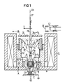
- a spectrometer lens according to the invention for the electron beam measurement technology consists of a short focal length, largely asymmetrical objective lens OL with an integrated electrostatic counterfield spectrometer and a single-stage deflection unit DS arranged symmetrically to the optical axis OA within the objective lens.
- the system consisting of objective lens OL, spectrometer and deflection unit DS forms the component of the electron-optical column of an electron steel measuring device with which the primary electrons emanating from a high-current electron source are focused and deflected and the secondary electrons SE triggered on the sample IC, for example an integrated circuit, into one point ZS lying on the optical axis OA are mapped.
- the electron source or its intermediate image ZP which is reduced by condenser lenses, is reduced again using the spectrometer objective onto the sample IC arranged in the immediate vicinity of the rear focal plane of the magnetic lens OL.
- the positioning of the primary electron steel PE on a point of the sample IC, which is not described in more detail, or its line-shaped deflection over the sample surface, is carried out with the aid of the deflection unit DS consisting of magnetic and electrical deflection elements MD or ED, the deflection main plane of which coincides approximately with the image-side main plane of the spectrometer objective.
- the position of this focusing point ZS which is to be interpreted as a real intermediate image of the virtual secondary electron source QS lying below the sample, is determined by the level of the suction voltage V E and the magnetic field strength, which is dependent on the primary electron energy, between the pole pieces of the objective lens OL.
- the virtual source QS is defined here by the smallest caustic cross section of all virtual secondary electron trajectories below the sample IC.
- the energy analysis of the secondary electrons SE takes place inside or above the objective lens OL in a spherically symmetrical electrical opposing field, which is built up in the space between two almost hemispherical network electrodes K1 and K2 which have different potentials.
- Such electrode assemblies are known for example from US-PS '4464571 known.
- the lower network electrode K1 is at the same potential V E as the suction electrode G1
- voltages V G between approximately -15 volts and + 15 volts are typically applied to the upper network electrode K2, which acts as a counter-field grid.
- a shielding grid BG can also be provided, which is supplied with approximately the same voltage V BG as the network electrode K2 (V BG ⁇ V G ).
- an annular detector DT arranged concentrically to the optical axis OA is provided within the spectrometer objective according to the invention.
- Semiconductor detectors, channel plates or metal plates with electron traps are particularly suitable for this.
- a second conventional detector for example consisting of suction electrode DE, scintillator SZ and light guide LL, can be provided above the spectrometer objective to detect the secondary electrons SE emitted in the direction of the optical axis OA.
- this intermediate image ZS must be sufficiently far above the pole pieces and the deflection unit DS in a field-free space in order to avoid Lamor rotations and the disturbances in the path movement of the secondary electrons SE caused by electrical fields after passing through the point ZS.
- the focusing of the secondary electrons SE in a point ZS lying on the optical axis OA above the deflection unit DS is the better possible the smaller the energy of the primary electrons PE and the higher the suction potential V E of the network electrode K1 which accelerates the secondary electrons SE.
- a hollow cylinder HZ consisting of three parts and arranged symmetrically to the optical axis OA is provided within the objective lens OL. While the upper part of this hollow cylinder, which tapers in the area of the pole shoes, is conductively connected to the spherical network electrode K1, its lower part, which partially protrudes from the objective lens OL, is terminated on the sample side by the flat suction electrode G1.
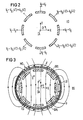
- an electrostatic eight-pole deflector is integrated into the middle part of this hollow cylinder HZ, which acts as a Faraday cage, by dividing this part of the tube in the z direction and azimuthally in accordance with the exemplary embodiment shown in FIG.
- the magnetic deflection element MD used advantageously is a saddle coil system manufactured in the manner of a flexible printed circuit board.
- the insulator located between the electrostatic deflection element ED and the deflection coils SPI, SPA was not shown in FIGS. 1 and 3 for reasons of clarity.
- the distribution of turns within the coil system should be selected so that the deflection unit generates a magnetic field that is as homogeneous as possible in a plane perpendicular to the optical axis OA.
- an electrical deflection field is intended on the optical axis OA and a magnetic abbot field be accepted.
- the Lorentz force acts on a charged particle of charge q and velocity V.
- the alignment condition for the deflection unit DS constructed in the manner of a Wien filter must not only be met for the maximum values of the electrical and magnetic field strength E o or B a, but also within the arrangement along the optical axis OA. As shown in FIG. 4, both the electrical and the magnetic deflection field E x (O, O, z) or By (0.0, z) drop in the direction of the sample IC - faster than in the direction of the intermediate image ZS.
- This asymmetrical field profile in the direction of the optical axis OA is a consequence of the structure of the spectrometer objective, in which the suction network G1 and the lower ball network K1 are at different distances from the electrical deflection element ED and the magnetic deflection element MD is arranged in the vicinity of the pole shoes.
- the exemplary embodiment of a spectrometer objective according to the invention shown in FIG. 5 consists of a short focal length objective lens OL, a deflection unit DS according to FIGS. 2 and 3 arranged symmetrically to the optical axis OA within the objective lens OL and an electrostatic counterfield spectrometer.
- the system consisting of objective lens OL, deflection unit DS and counter-field spectrometer forms the component of the electron-optical column of an electron beam measuring device, with which the primary electrons PE emitted by a high-current electron source are focused and deflected and the secondary electrons SE triggered on the sample IC into the one on the optical one Center ZS of the spherically symmetrical opposing field lying on the axis OA.
- the opposing electrical field is generated with the aid of the network electrodes K1 and K2 arranged in a housing GH above the objective lens OL, each of which has parts of the surface of concentric spheres with different radii R or R2 (R 1 ⁇ 30 mm, R 2 ⁇ 34 mm) form. Since the center point ZS defining the center of the opposing field of the balls assigned to the network electrodes K1 and K2 is very far above the deflection unit DS consisting of magnetic and electrical deflection elements MD or ED and the pole shoe gap, Larmor rotations of the secondary electrons SE are avoided after passing through the intermediate image ZS.
- one of three parts is inside the housing GH, which is closed by a ring-shaped secondary electron detector DT and in which, in addition to the network electrodes K1 and K2, there is also a shielding grid BG and a channel plate CP existing, symmetrical to the optical axis OA arranged hollow cylinder HZ seen before. While the upper part of this hollow cylinder HZ, which tapers in the area of the objective lens OL, is conductively connected to the network electrode K1, which is at a potential V E , the lower part of the latter is on the sample side, likewise between 0.5 and 5 kV, at the potential V E , in particular 2 kV network electrode G1 completed.
- the middle cylinder part is again designed as an electrostatic eight-pole deflector ED according to FIG. 2, and is enclosed by the magnetic deflection element MD shown in FIG. 3.
Landscapes
- Chemical & Material Sciences (AREA)
- Analytical Chemistry (AREA)
- Engineering & Computer Science (AREA)
- General Engineering & Computer Science (AREA)
- Physics & Mathematics (AREA)
- General Physics & Mathematics (AREA)
- Electron Tubes For Measurement (AREA)
- Analysing Materials By The Use Of Radiation (AREA)
- Tests Of Electronic Circuits (AREA)
- Testing Or Measuring Of Semiconductors Or The Like (AREA)
Applications Claiming Priority (2)
| Application Number | Priority Date | Filing Date | Title |
|---|---|---|---|
| DE3607553 | 1986-03-07 | ||
| DE3607553 | 1986-03-07 |
Publications (2)
| Publication Number | Publication Date |
|---|---|
| EP0236807A2 true EP0236807A2 (fr) | 1987-09-16 |
| EP0236807A3 EP0236807A3 (fr) | 1990-05-16 |
Family
ID=6295767
Family Applications (1)
| Application Number | Title | Priority Date | Filing Date |
|---|---|---|---|
| EP87102318A Withdrawn EP0236807A3 (fr) | 1986-03-07 | 1987-02-18 | Objectif de spectromètre en technique de mesure par faisceau corpusculaire |
Country Status (4)
| Country | Link |
|---|---|
| US (1) | US4769543A (fr) |
| EP (1) | EP0236807A3 (fr) |
| JP (1) | JPS62219446A (fr) |
| CA (1) | CA1253636A (fr) |
Cited By (1)
| Publication number | Priority date | Publication date | Assignee | Title |
|---|---|---|---|---|
| EP2043130A3 (fr) * | 2007-09-25 | 2010-11-24 | Ceos Corrected Electron Optical Systems GmbH | Bobines multipolaires |
Families Citing this family (15)
| Publication number | Priority date | Publication date | Assignee | Title |
|---|---|---|---|---|
| GB2201288B (en) * | 1986-12-12 | 1990-08-22 | Texas Instruments Ltd | Electron beam apparatus |
| US4983833A (en) * | 1988-11-21 | 1991-01-08 | Siemens Aktiengesellschaft | Device for the detecting of charged secondary particles |
| CA1317035C (fr) * | 1989-01-25 | 1993-04-27 | Matthias Brunner | Methode pour examiner un specimen dans un appareil a faisceau de particules |
| US5079428A (en) * | 1989-08-31 | 1992-01-07 | Bell Communications Research, Inc. | Electron microscope with an asymmetrical immersion lens |
| JP3148353B2 (ja) * | 1991-05-30 | 2001-03-19 | ケーエルエー・インストルメンツ・コーポレーション | 電子ビーム検査方法とそのシステム |
| JP3730263B2 (ja) * | 1992-05-27 | 2005-12-21 | ケーエルエー・インストルメンツ・コーポレーション | 荷電粒子ビームを用いた自動基板検査の装置及び方法 |
| JP3291880B2 (ja) * | 1993-12-28 | 2002-06-17 | 株式会社日立製作所 | 走査形電子顕微鏡 |
| DE4438315A1 (de) * | 1994-10-26 | 1996-05-02 | Siemens Ag | Vorrichtung zum Entfernen von Ionen aus einem Elektronenstrahl |
| EP0821393B1 (fr) * | 1996-07-25 | 1999-06-16 | ACT Advanced Circuit Testing Gesellschaft für Testsystementwicklung mbH | Lentille objectif de détecteur |
| WO2000002230A1 (fr) * | 1998-07-02 | 2000-01-13 | Institut De Microtechnique | Detecteur d'electrons |
| US6787772B2 (en) * | 2000-01-25 | 2004-09-07 | Hitachi, Ltd. | Scanning electron microscope |
| TW579536B (en) * | 2001-07-02 | 2004-03-11 | Zeiss Carl Semiconductor Mfg | Examining system for the particle-optical imaging of an object, deflector for charged particles as well as method for the operation of the same |
| EP1517353B1 (fr) * | 2003-09-11 | 2008-06-25 | ICT Integrated Circuit Testing Gesellschaft für Halbleiterprüftechnik mbH | Système pour reduire la dispersion en énergie d'un faisceau de particules chargées pour un système à faisceau de particules chargées |
| JP4316394B2 (ja) * | 2004-01-21 | 2009-08-19 | 株式会社東芝 | 荷電ビーム装置 |
| US10319578B2 (en) * | 2016-01-21 | 2019-06-11 | Japan Synchrotron Radiation Research Institute | Retarding potential type energy analyzer |
Citations (6)
| Publication number | Priority date | Publication date | Assignee | Title |
|---|---|---|---|---|
| DE1089088B (de) * | 1956-07-10 | 1960-09-15 | Siemens Ag | Anordnung zur Objektbeleuchtung im Elektronenmikroskop |
| EP0097535A2 (fr) * | 1982-06-23 | 1984-01-04 | Fujitsu Limited | Filtre de vitesse à champs croisés et système de traitememnt avec faisceau d'ions |
| US4464571A (en) * | 1981-09-30 | 1984-08-07 | Siemens Aktiengesellschaft | Opposing field spectrometer for electron beam mensuration technology |
| US4525629A (en) * | 1981-06-15 | 1985-06-25 | Nippon Telegraph & Telephone Public Corporation | Deflective focusing system for charged particle beam |
| US4540885A (en) * | 1982-09-30 | 1985-09-10 | Siemens Aktiengesellschaft | Spectrometer objective having parallel objective fields and spectrometer fields for the potential measuring technique |
| WO1985004757A1 (fr) * | 1984-04-06 | 1985-10-24 | Hitachi, Ltd. | Detecteur d'electrons secondaires |
Family Cites Families (7)
| Publication number | Priority date | Publication date | Assignee | Title |
|---|---|---|---|---|
| DE241812C (fr) * | 1909-06-11 | |||
| US3930181A (en) * | 1973-12-28 | 1975-12-30 | Ibm | Lens and deflection unit arrangement for electron beam columns |
| NL7415318A (nl) * | 1974-11-25 | 1976-05-28 | Philips Nv | Wienfilter. |
| US4590379A (en) * | 1980-09-16 | 1986-05-20 | Martin Frederick W | Achromatic deflector and quadrupole lens |
| US4395691A (en) * | 1982-03-04 | 1983-07-26 | Hughes Aircraft Company | Beam deflection system |
| EP0175933A1 (fr) * | 1984-09-21 | 1986-04-02 | Siemens Aktiengesellschaft | Système de lentilles à balayage sans défauts chromatiques de déviation pour traitement de matériaux par faisceaux corpusculaires |
| DE3521464A1 (de) * | 1985-06-14 | 1986-12-18 | Siemens AG, 1000 Berlin und 8000 München | Spektrometer-objektiv fuer die elektronenstrahl-messtechnik |
-
1987
- 1987-02-18 EP EP87102318A patent/EP0236807A3/fr not_active Withdrawn
- 1987-03-04 JP JP62049896A patent/JPS62219446A/ja active Pending
- 1987-03-05 CA CA000531181A patent/CA1253636A/fr not_active Expired
- 1987-03-09 US US07/023,857 patent/US4769543A/en not_active Expired - Fee Related
Patent Citations (6)
| Publication number | Priority date | Publication date | Assignee | Title |
|---|---|---|---|---|
| DE1089088B (de) * | 1956-07-10 | 1960-09-15 | Siemens Ag | Anordnung zur Objektbeleuchtung im Elektronenmikroskop |
| US4525629A (en) * | 1981-06-15 | 1985-06-25 | Nippon Telegraph & Telephone Public Corporation | Deflective focusing system for charged particle beam |
| US4464571A (en) * | 1981-09-30 | 1984-08-07 | Siemens Aktiengesellschaft | Opposing field spectrometer for electron beam mensuration technology |
| EP0097535A2 (fr) * | 1982-06-23 | 1984-01-04 | Fujitsu Limited | Filtre de vitesse à champs croisés et système de traitememnt avec faisceau d'ions |
| US4540885A (en) * | 1982-09-30 | 1985-09-10 | Siemens Aktiengesellschaft | Spectrometer objective having parallel objective fields and spectrometer fields for the potential measuring technique |
| WO1985004757A1 (fr) * | 1984-04-06 | 1985-10-24 | Hitachi, Ltd. | Detecteur d'electrons secondaires |
Non-Patent Citations (2)
| Title |
|---|
| SIEMENS FORSCHUNGS- UND ENTWICKLUNGSBERICHTE, vol. 16, no. 1, 1987, Seiten 30-36, Berlin, Heidelberg, DE; E. PLIES et al.: "Calculation of fields and secondary electron trajectories in a new in-lens spectrometer for electron beam testing" * |
| SOLID STATE TECHNOLOGY, vol. 28, no. 12, 1985, seiten 63-70, Port Washington, New York, US; E. MENZEL et al.: "Electron beam probing of integrated circuits" * |
Cited By (1)
| Publication number | Priority date | Publication date | Assignee | Title |
|---|---|---|---|---|
| EP2043130A3 (fr) * | 2007-09-25 | 2010-11-24 | Ceos Corrected Electron Optical Systems GmbH | Bobines multipolaires |
Also Published As
| Publication number | Publication date |
|---|---|
| JPS62219446A (ja) | 1987-09-26 |
| US4769543A (en) | 1988-09-06 |
| CA1253636A (fr) | 1989-05-02 |
| EP0236807A3 (fr) | 1990-05-16 |
Similar Documents
| Publication | Publication Date | Title |
|---|---|---|
| EP0333018B1 (fr) | Lentille d'objectif pour la focalisation de particules chargées | |
| EP0267555B1 (fr) | Objectif de spectromètre pour appareils de mesure par faisceau corpusculaire et procédé pour l'examen d'échantillons. | |
| EP0281743B1 (fr) | Objectif détecteur pour microscope à balayage | |
| EP0461442B1 (fr) | Appareil à faisceau de particules | |
| EP0205184B1 (fr) | Objectif de faible aberration comportant un spectromètre de haute acceptance en électrons secondaires | |
| EP0893816B1 (fr) | Appareil à faisceau corpusculaire | |
| DE69822139T2 (de) | Korrekturvorrichtung zur linsenfehlerkorrektur in ladungsträger-optischen geräten | |
| EP0274622B1 (fr) | Assemblage de détecteur avec un objectif muni d'un détecteur pour instruments à rayons corpusculaires | |
| EP0242602B1 (fr) | Lentille électrostatique et magnétique pour appareils à faisceau corpusculaire | |
| EP1220292B1 (fr) | Monochromateur pour particules chargées | |
| EP0236807A2 (fr) | Objectif de spectromètre en technique de mesure par faisceau corpusculaire | |
| EP0370276B1 (fr) | Dispositif pour détecter des particules chargées secondaires | |
| DE3532781A1 (de) | Anordnung zur detektion von sekundaer- und/oder rueckstreuelektronen in einem elektronenstrahlgeraet | |
| DE69920182T2 (de) | Korpuskularstrahloptisches gerät mit auger-elektronendetektion | |
| DE112015001235B4 (de) | Vorrichtung und verfahren zur abbildung mittels eines elektronenstrahls unter verwendung eines monochromators mit doppeltem wien-filter sowie monochromator | |
| EP0105439B1 (fr) | Objectif de spectromètre à champs d'objectif et de spectromètre parallèles utilisé en technique de mesure de potentiel | |
| EP0205185B1 (fr) | Objectif comportant un spectromètre en technique de mesure par faisceau d'électrons | |
| EP0194570A2 (fr) | Microscope corpusculaire à balayage à effet Boersch réduit | |
| DE112017007063T5 (de) | Ladungsträgerstrahlvorrichtung | |
| DE69117347T2 (de) | Energie-Analysatoren für Ladungsträgerpartikel | |
| DE3703028A1 (de) | Rastermikroskop | |
| DE69606515T2 (de) | Elektrostatisch-magnetische Linsenanordnung | |
| DE69501533T2 (de) | Partikel-optisches instrument mit einer ablenkeinheit für sekundärelektronen | |
| EP0086431A2 (fr) | Système générateur de faisceau de particules et méthode d'utilisation | |
| DE10235981B4 (de) | Teilchenoptische Vorrichtung und Elektronenmikroskop |
Legal Events
| Date | Code | Title | Description |
|---|---|---|---|
| PUAI | Public reference made under article 153(3) epc to a published international application that has entered the european phase |
Free format text: ORIGINAL CODE: 0009012 |
|
| AK | Designated contracting states |
Kind code of ref document: A2 Designated state(s): AT BE CH DE FR GB IT LI LU NL SE |
|
| PUAL | Search report despatched |
Free format text: ORIGINAL CODE: 0009013 |
|
| AK | Designated contracting states |
Kind code of ref document: A3 Designated state(s): AT BE CH DE FR GB IT LI LU NL SE |
|
| 17P | Request for examination filed |
Effective date: 19901107 |
|
| 17Q | First examination report despatched |
Effective date: 19930121 |
|
| STAA | Information on the status of an ep patent application or granted ep patent |
Free format text: STATUS: THE APPLICATION IS DEEMED TO BE WITHDRAWN |
|
| 18D | Application deemed to be withdrawn |
Effective date: 19930602 |
|
| RIN1 | Information on inventor provided before grant (corrected) |
Inventor name: PLIES, ERICH DR. RER. NAT. |