EP0226128A2 - Alimentation à découpage électronique - Google Patents
Alimentation à découpage électronique Download PDFInfo
- Publication number
- EP0226128A2 EP0226128A2 EP86116807A EP86116807A EP0226128A2 EP 0226128 A2 EP0226128 A2 EP 0226128A2 EP 86116807 A EP86116807 A EP 86116807A EP 86116807 A EP86116807 A EP 86116807A EP 0226128 A2 EP0226128 A2 EP 0226128A2
- Authority
- EP
- European Patent Office
- Prior art keywords
- battery
- transistor
- voltage
- capacitor
- resistor
- Prior art date
- Legal status (The legal status is an assumption and is not a legal conclusion. Google has not performed a legal analysis and makes no representation as to the accuracy of the status listed.)
- Granted
Links
Images
Classifications
-
- H—ELECTRICITY
- H02—GENERATION; CONVERSION OR DISTRIBUTION OF ELECTRIC POWER
- H02J—CIRCUIT ARRANGEMENTS OR SYSTEMS FOR SUPPLYING OR DISTRIBUTING ELECTRIC POWER; SYSTEMS FOR STORING ELECTRIC ENERGY
- H02J7/00—Circuit arrangements for charging or depolarising batteries or for supplying loads from batteries
- H02J7/02—Circuit arrangements for charging or depolarising batteries or for supplying loads from batteries for charging batteries from ac mains by converters
-
- H—ELECTRICITY
- H02—GENERATION; CONVERSION OR DISTRIBUTION OF ELECTRIC POWER
- H02M—APPARATUS FOR CONVERSION BETWEEN AC AND AC, BETWEEN AC AND DC, OR BETWEEN DC AND DC, AND FOR USE WITH MAINS OR SIMILAR POWER SUPPLY SYSTEMS; CONVERSION OF DC OR AC INPUT POWER INTO SURGE OUTPUT POWER; CONTROL OR REGULATION THEREOF
- H02M3/00—Conversion of dc power input into dc power output
- H02M3/22—Conversion of dc power input into dc power output with intermediate conversion into ac
- H02M3/24—Conversion of dc power input into dc power output with intermediate conversion into ac by static converters
- H02M3/28—Conversion of dc power input into dc power output with intermediate conversion into ac by static converters using discharge tubes with control electrode or semiconductor devices with control electrode to produce the intermediate ac
- H02M3/325—Conversion of dc power input into dc power output with intermediate conversion into ac by static converters using discharge tubes with control electrode or semiconductor devices with control electrode to produce the intermediate ac using devices of a triode or a transistor type requiring continuous application of a control signal
- H02M3/335—Conversion of dc power input into dc power output with intermediate conversion into ac by static converters using discharge tubes with control electrode or semiconductor devices with control electrode to produce the intermediate ac using devices of a triode or a transistor type requiring continuous application of a control signal using semiconductor devices only
- H02M3/33507—Conversion of dc power input into dc power output with intermediate conversion into ac by static converters using discharge tubes with control electrode or semiconductor devices with control electrode to produce the intermediate ac using devices of a triode or a transistor type requiring continuous application of a control signal using semiconductor devices only with automatic control of the output voltage or current, e.g. flyback converters
-
- H—ELECTRICITY
- H02—GENERATION; CONVERSION OR DISTRIBUTION OF ELECTRIC POWER
- H02J—CIRCUIT ARRANGEMENTS OR SYSTEMS FOR SUPPLYING OR DISTRIBUTING ELECTRIC POWER; SYSTEMS FOR STORING ELECTRIC ENERGY
- H02J2207/00—Indexing scheme relating to details of circuit arrangements for charging or depolarising batteries or for supplying loads from batteries
- H02J2207/20—Charging or discharging characterised by the power electronics converter
-
- H—ELECTRICITY
- H02—GENERATION; CONVERSION OR DISTRIBUTION OF ELECTRIC POWER
- H02M—APPARATUS FOR CONVERSION BETWEEN AC AND AC, BETWEEN AC AND DC, OR BETWEEN DC AND DC, AND FOR USE WITH MAINS OR SIMILAR POWER SUPPLY SYSTEMS; CONVERSION OF DC OR AC INPUT POWER INTO SURGE OUTPUT POWER; CONTROL OR REGULATION THEREOF
- H02M1/00—Details of apparatus for conversion
- H02M1/0003—Details of control, feedback or regulation circuits
- H02M1/0032—Control circuits allowing low power mode operation, e.g. in standby mode
-
- Y—GENERAL TAGGING OF NEW TECHNOLOGICAL DEVELOPMENTS; GENERAL TAGGING OF CROSS-SECTIONAL TECHNOLOGIES SPANNING OVER SEVERAL SECTIONS OF THE IPC; TECHNICAL SUBJECTS COVERED BY FORMER USPC CROSS-REFERENCE ART COLLECTIONS [XRACs] AND DIGESTS
- Y02—TECHNOLOGIES OR APPLICATIONS FOR MITIGATION OR ADAPTATION AGAINST CLIMATE CHANGE
- Y02B—CLIMATE CHANGE MITIGATION TECHNOLOGIES RELATED TO BUILDINGS, e.g. HOUSING, HOUSE APPLIANCES OR RELATED END-USER APPLICATIONS
- Y02B70/00—Technologies for an efficient end-user side electric power management and consumption
- Y02B70/10—Technologies improving the efficiency by using switched-mode power supplies [SMPS], i.e. efficient power electronics conversion e.g. power factor correction or reduction of losses in power supplies or efficient standby modes
Definitions
- the invention relates to an electronic switching power supply for charging a battery or an accumulator from an AC or DC voltage source of different voltage levels with a primary clocked flyback converter, in which the primary winding of a transformer in series with a first transistor and its secondary winding in series with the battery and one is connected to the first diode, the base of the first transistor being connected via the series connection of a first capacitor and a first resistor to one winding end of the secondary winding of the transmitter, the other winding end of which is connected to the battery, and also via a second resistor having one pole the input voltage source and is connected to the collector of a second transistor whose emitter is connected to reference potential, and wherein the emitter of the first transistor is connected to the Ba both via a third resistor with reference potential and via a Zener diode sis of the second transistor is connected, which is connected via a fourth resistor to reference potential.
- An electronic switching power supply of the type mentioned is known from DE-OS 32 18 594, which is used for quick charging and trickle charging of a battery, preferably a nickel-cadmium battery, the electronic switching power supply basically for constant voltage and / or constant current supply of electrical or electronic Devices provided and is constructed as a primary clocked flyback converter.
- the primary winding of a transformer is in series a switching transistor and the secondary winding of the transmitter in series with an electrical consumer in the form of the parallel connection of a battery and an electric motor and a diode.
- the known electronic switching power supply includes a voltage comparator, which consists of two transistors including the associated wiring and monitors the set voltage setpoint at consumers and the switching transistor of the barrier wall when it reaches this setpoint - toddlers locks.
- a voltage comparator which consists of two transistors including the associated wiring and monitors the set voltage setpoint at consumers and the switching transistor of the barrier wall when it reaches this setpoint - toddlers locks.
- a circuit arrangement for the regulated supply of a consumer which can be operated at different direct or alternating voltages as well as at different alternating current frequencies without switching.
- This known circuit arrangement has a flyback converter which is controlled by means of two controllable semiconductor switches as a function of the current flowing through the primary winding of a transmitter and as a function of the input voltage supplied in such a way that the output power output is almost constant.
- the parallel connection of a battery with a direct current motor is provided as the consumer, so that the circuit arrangement supplies either the full motor power during mains operation or a charging current for the battery when the motor is switched off. When the DC motor is switched off, the nickel-cadmium battery is charged quickly with high current.
- a voltage-dependent switch is provided in this known circuit arrangement, which consists of a transistor, the collector of which is connected via a resistor to the base of the switching transistor connected in series with the transmitter and the base-emitter Route is connected in series with another resistor and a Zener diode in parallel to the battery to be charged. If the battery voltage exceeds the value specified by the zener diode during the rapid charging process, the transistor switches through and thus blocks the switching transistor connected in series with the primary winding of the transmitter.
- the respective switch-on and switch-off times of the flyback converter depend on the currents flowing through two different resistors, so that a hysteresis behavior results from the difference between these currents.
- the flyback converter does not constantly switch back and forth between an switched-on and a switched-off state, but instead requires that the battery voltage must have decreased by a certain amount before the charging current is switched on again.
- a light-emitting diode arranged in the base circuit of the second transistor also goes out and thus indicates the end of the charging process.
- This circuit arrangement for fast charging a battery by means of a primary clocked flyback converter has a relatively low efficiency owing to the required standby voltage for the control and regulating electronics and, moreover, requires a constant current draw from the battery for operating the control when the mains plug is pulled, ie when the battery is operated purely. and control electronics. In addition, the expenditure on components is relatively large.
- the object of the present invention is to provide an electronic switching power supply for charging a battery from an AC or DC voltage source of different voltage levels, which switches the charging current on and off practically without loss and does not consume any energy when it is not connected to the supply voltage.
- the solution according to the invention ensures that no energy is consumed when the switched-mode power supply is switched off, since the battery is disconnected from the switching device and therefore cannot be discharged.
- an advantageous embodiment of the solution according to the invention is that the switching device connects the decoupling device to the reference potential when the switched-mode power supply is switched off. This ensures that after the switching power supply is switched on, the flyback converter immediately vibrates continuously and a large charging current flows.
- a further advantageous embodiment is characterized in that the switching device consists of an auxiliary voltage circuit which is acted upon by the battery voltage and which switches over as a function of the charging characteristics of the battery when the battery is fully charged.
- This configuration enables the full charge of a battery, for example a nickel-cadmium battery, to be reached with a constant charging current irrespective of the age of the battery and changes in the charging characteristics of the battery.
- the switching device consists of a self-holding thermal switch, which is influenced by the cell temperature of the battery and switches depending on the charging characteristics of the battery when the battery is fully charged.
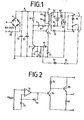
- the electronic switching power supply shown in Fig. 1 has a primary clocked flyback converter with a transformer 5 and a first transistor 1 and a first diode 31 provided in the load circuit, which is polarized so that the stored in the blocking time of the first transistor 1 in the transformer 5 Energy in the load 6, which consists of a battery 61 and a DC motor 62 which can be switched to the battery 61 via a switch 63, is discharged.
- the flyback converter is fed via a rectifier bridge circuit 4 and a resistor 28 from a direct or alternating voltage network, the voltage of which varies between 100 and 250 volts, in extreme cases also 12 volts, and the frequency of which can be almost arbitrary in the case of a feeding alternating voltage network can.
- the rectified output voltage is applied to the input of the flyback converter or the control and regulating electronics via a filter and smoothing circuit, which consists of a series choke 8 and two smoothing capacitors 91, 92.
- the series connection of the primary winding 51 of the transformer 5 with the collector-emitter path of the first transistor 1 is connected in parallel with the DC voltage terminals.
- the base of the first transistor 1 is connected via the series connection of a first capacitor 11 and a first resistor 21 to the one connection of the secondary winding 52 of the transformer 5 and also via a second resistor 22 and the series reactor 8 to the positive pole of the input voltage terminal.
- the base of the first transistor 1 is connected to ground or reference potential via the collector-emitter path of a second transistor 2.
- the emitter of the first transistor 1 is connected to the cathode of a first zener diode 41, the anode of which is connected both to the base of the second transistor 2 and to a ground or reference potential via the parallel connection of a fourth resistor 24 and a further capacitor 13.
- the emitter of the first transistor 1 is connected to ground or reference potential via a third resistor 23.
- the winding direction of the primary and secondary windings 51 and 52 of the transformer 5 is determined by the points entered.
- the second capacitor 12 is connected to the connection terminals A and B of a switching device 7, the third connection terminal C of which is connected via the series connection of a fifth resistor 25 with a third diode 33 to the connection of the anode of the Zener diode 41 to the base of the second transistor 2, wherein the cathode of the third diode 33 is connected to the anode of the zener diode 41.
- the switching device 7 is such that the third connection terminal C is connected either to the connection terminal A or to the connection terminal B, in which case the connection terminal A can be connected to the connection terminal C via a further diode 35.
- the first transistor 1 operating as a switching transistor is switched via the second resistor 22 with a low base current driven, as a result of which the first transistor 1 is driven into the conductive state.
- the collector current increases linearly and generates a voltage proportional to the respective collector current at the third resistor 23.
- the second transistor When a specific peak current value of the collector current or a correspondingly proportional voltage is reached, the second transistor is driven via the zener diode 41, thereby becoming conductive and connecting the base of the first transistor 1 to ground or reference potential and thus removing the first transistor 1 the base current, whereupon the first transistor 1 blocks.
- the polarity of the voltage induced in the secondary winding 52 of the transformer 5 changes.
- the energy stored in the transmitter 5 is thus emitted to the battery 61 via the first diode 31 according to the principle of the flyback converter.
- the series connection of the diode 34 with the zener diode 42 connected in parallel with the primary winding 51 of the transformer 5 limits the switch-back voltage peak during the blocking phase of the first transistor 1, the diode 34 and the zener diode 42 being connected together either on the cathode side or on the anode side.
- the first capacitor 11 In the conducting state of the first transistor 1, the first capacitor 11 is charged via the first resistor 21 and, in the blocking state of the first transistor 1, is recharged in such a way that a positive voltage is present at its electrode connected to the base of the first transistor 1, which also operates at very low operation voltage of z. B. 12 volts ensures an immediate reactivation of the first transistor 1 when the second transistor 2 blocks after the end of the transmitter discharge phase and thus the first transistor 1 is controlled in the conducting state.
- the battery 61 is rapidly charged, the battery charging current being determined by the primary-side peak current and the inductance of the transmitter.
- the voltage across the second capacitor 12 is where U Batt is the voltage on the battery 61, Uf31 is the forward voltage drop of the first diode 31 and U f32 is the forward voltage drop of the second diode 32.
- U Batt is the voltage on the battery 61
- Uf31 is the forward voltage drop of the first diode 31
- U f32 is the forward voltage drop of the second diode 32.
- the battery 61 is charged with a trickle charge current
- the voltage at the second capacitor 12 is, where U BET2 the base-emitter voltage drop across the second transistor, R 24 the resistance value of the fourth resistor of the 24, R 25 the resistance value of the fifth resistor 25, U f33 the voltage drop at the third diode 33 and U f35 the forward voltage drop at the fifth diode 35 means.
- a charging current always flows into the battery 61 when the sum of the voltage at the second capacitor 12 U CEL and U f32 is greater than the sum of the voltage at the battery U Batt and the forward voltage drop U f31 at the first Diode 31. This means that the charge current is drastically reduced compared to the charge current in the fast charge state during the trickle charge state. In both switching positions of the switching device 7, however, a voltage is available on the second capacitor 12.
- the first transistor 1 always switches to the conducting state when the base voltage of the second transistor 2 drops below a certain voltage value specified by the zener diode 41, so that the second transistor 2 blocks, and thus, during the discharge of the transformer 5 the first transistor 1 is controlled into the conductive state via the second resistor 22 and with the support of the correspondingly reversed charge in the first capacitor 11.
- FIG. 2 shows a switching device which detects the cell voltage of the battery 61 and switches over at a specific cell voltage value. It contains a differential amplifier 71, the positive input of which with the is applied to the upper pole of the battery 61, while the negative input is connected to the lower pole of the battery 61 via a third capacitor 73 and to its output via a fourth diode 72, the anode of the fourth diode 72 being connected to the output of the differential amplifier 71 is.
- the output of the differential amplifier 71 is connected to the base of a third transistor 74, the collector of which is connected to the base of a fourth transistor 89 and is connected via a sixth resistor 75 to the collector of the fourth transistor 89 and forms the connection terminal A according to FIG. 1 .
- the emitter of transistor 89 which forms terminal C according to FIG. 1, is connected via a resistor 90 to ground or reference potential, which represents terminal B.
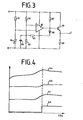
- FIG. 4 shows the charging characteristics, for example of a nickel-cadmium battery, which should preferably be charged with a constant or almost constant charging current.
- 4 shows the cell voltage (curve 4a), the cell temperature (curve 4b) and the internal gas pressure (curve 4c) of a nickel-cadmium battery over the charging time t. It should be taken into account that both the cell voltage and the cell temperature and the internal gas pressure during the charging process can vary depending on the charging current and the ambient temperature.
- the amplitudes of curves 4a, 4b and 4c can also change when the battery ages, but the curve shape, ie above all the pronounced maximum, is retained.
- the cell voltage shows a short pronounced maximum when the full charge is reached and then drops to a value which is higher than the value before the full charge was reached.
- This pronounced maximum is used in the circuit arrangement according to FIG. 2, which in the actual sense is to be regarded as a peak voltage meter and, according to curve 4d, topples over when the maximum is reached, since with falling voltage at the positive input of the comparator 71 the voltage present at the charged third capacitor 73 predominates and thus can swing the comparator output.
- the exemplary embodiment of the switching device 7 shown in FIG. 3 shows a self-holding thermal switch which uses the course of the cell temperature of a battery when the fully charged state is reached.
- first voltage divider connected in parallel with the second capacitor 12, which consists of a first voltage divider resistor 81 and a temperature-dependent resistor 84, which is thermally connected to the battery 61, and a second, likewise parallel to the second capacitor 12 connected voltage divider, which consists of the series connection of a second voltage divider resistor 82 and a third voltage divider resistor 83.
- the first voltage divider resistor is connected to the negative input of a comparator 80, while the second voltage divider is connected to the% positive input of the comparator 80.
- the output of the comparator 80 is connected via a diode 88 and a resistor 85 to the positive input of the comparator 80 bound, a capacitor 86 being connected in parallel with the third voltage divider resistor 83.
- the output of the comparator 80 is connected to the base of a transistor 89, the collector of which forms the connection terminal A according to FIG. 1, while the emitter forms the connection terminal C according to FIG. 1.
- the emitter of transistor 89 is connected to ground or reference potential via a resistor 90 and thus forms the connection terminal B according to FIG. 1.
- a further resistor 87 is connected in parallel with the base-collector path of transistor 89.
- the self-holding thermal switch shown in Fig. 3 is designed so that the output of the comparator jumps to a high voltage level when a predetermined cell temperature is exceeded, ensuring that a low tolerance of the switching temperature is achieved without adjustment. If the comparator 80 is connected to the operating voltage, the voltage at the non-inverting input of the comparator 80 is lower than that of the inverting input of the comparator until the second capacitor 12 is charged. The output of the comparator thus tilts into a position with a low voltage level.
- the output of the comparator 80 remains at a low voltage level as long as the resistance value of the temperature-dependent resistor 84 is greater than the resistance value of the third voltage divider resistor 83.
- the comparator output tilts into one position high voltage level, as a result of which the series connection of the resistor 85 with the diode 88 is connected in parallel to the second voltage divider resistor 82 and the output of the comparator 80 remains at a high voltage level for as long as the temperature-dependent resistor 84 is required in order to become more high-resistance again due to the cooling.
- This ensures that the cell temperature shown in curve 4b of FIG. 4 over the charging time with a small tolerance of the switching temperature and without adjustment of the electronic switching power supply is exactly taken into account and leads to a corresponding switchover of the electronic switching power supply when the temperature jumps at the time of full charge.
- the flyback converter oscillates unaffected by the output voltage or the output current when the base of the transistor 2 is connected to the terminal B via the decoupling diode 33, that is to say Reference potential is. If the forward voltages of the diodes 31 and 32 are neglected, the voltage across the capacitor 12 is equal to the terminal voltage of the accumulator 61. If the base of the transistor 2 is connected to the positive pole of the capacitor 12 (terminal A) via the decoupling diode 33, the transistor 2 becomes conductive and thus the flyback converter is put out of operation. The voltage across the capacitor 12 and the base voltage of the transistor 2, which is proportional to this, then decreases in accordance with its discharge time constant. If the base voltage falls below the value at which transistor 2 conducts, it is blocked and the flyback converter starts to work again. The voltage across the capacitor 12 consequently rises until the transistor 2 conducts again and puts the flyback converter out of operation again.
- the arithmetic mean of the base voltage of transistor 2 is equal to the base-emitter voltage at which this transistor conducts (approx. 0.6 V).
- the arithmetic mean of the voltage across capacitor 12 is proportional to the base voltage. Since the discharge time constant of the capacitor 12 is large, there are correspondingly large pauses between the individual charge current pulses of this capacitor, so that the arithmetic mean of this current and the charge current of the accumulator 61 is very small. The pulse-pause ratio of the battery charging current is therefore corresponding to that of the capacitor charging current.
- the switching device 7 Since the switching device 7, which is generally an electronic switch and requires an operating voltage, receives this operating voltage from the capacitor 12 and not from the battery 61, it only functions when the switched-mode power supply is connected to the supply voltage. If the switching power supply is disconnected from the supply voltage, the voltage across the capacitor 12 becomes zero. There is no galvanic connection between the switching device 7 and the accumulator 61, which is why the accumulator cannot be discharged either.
- the switching device 7 can thus be designed so that it switches the switching power supply from a high fast charging current to a low trickle charging current and vice versa depending on the cell voltage, the cell temperature or the internal gas pressure of the battery.
Priority Applications (1)
| Application Number | Priority Date | Filing Date | Title |
|---|---|---|---|
| AT86116807T ATE43209T1 (de) | 1985-12-20 | 1986-12-03 | Elektronisches schaltnetzteil. |
Applications Claiming Priority (2)
| Application Number | Priority Date | Filing Date | Title |
|---|---|---|---|
| DE3545324 | 1985-12-20 | ||
| DE19853545324 DE3545324A1 (de) | 1985-12-20 | 1985-12-20 | Elektronisches schaltnetzteil |
Publications (4)
| Publication Number | Publication Date |
|---|---|
| EP0226128A2 true EP0226128A2 (fr) | 1987-06-24 |
| EP0226128A3 EP0226128A3 (en) | 1988-08-31 |
| EP0226128B1 EP0226128B1 (fr) | 1989-05-17 |
| EP0226128B2 EP0226128B2 (fr) | 1994-05-11 |
Family
ID=6289100
Family Applications (1)
| Application Number | Title | Priority Date | Filing Date |
|---|---|---|---|
| EP86116807A Expired - Lifetime EP0226128B2 (fr) | 1985-12-20 | 1986-12-03 | Alimentation à découpage électronique |
Country Status (4)
| Country | Link |
|---|---|
| US (1) | US4706009A (fr) |
| EP (1) | EP0226128B2 (fr) |
| AT (1) | ATE43209T1 (fr) |
| DE (2) | DE3545324A1 (fr) |
Cited By (6)
| Publication number | Priority date | Publication date | Assignee | Title |
|---|---|---|---|---|
| WO1989007854A1 (fr) * | 1988-02-09 | 1989-08-24 | Braun Aktiengesellschaft | Procede et circuits de determination de la duree de chargement d'accumulateurs |
| EP0383381A1 (fr) * | 1989-02-14 | 1990-08-22 | Koninklijke Philips Electronics N.V. | Circuit d'alimentation |
| EP0548749A1 (fr) * | 1991-12-24 | 1993-06-30 | FIAT AUTO S.p.A. | Circuit électronique d'alimentation à courant continu pour charges électriques et spécialement pour véhicule à propulsion électrique à alimentation par accumulateurs |
| WO1995012840A1 (fr) * | 1993-11-03 | 1995-05-11 | Braun Aktiengesellschaft | Alimentation a decoupage |
| WO1995013645A1 (fr) * | 1993-11-09 | 1995-05-18 | Braun Aktiengesellschaft | Circuit de declenchement d'un circuit de courant de charge pour accumulateur |
| CN108695953A (zh) * | 2017-04-05 | 2018-10-23 | 赛米控电子股份有限公司 | 用于给车辆供电的功率转换器装置和包括该装置的设备 |
Families Citing this family (10)
| Publication number | Priority date | Publication date | Assignee | Title |
|---|---|---|---|---|
| US5266881A (en) * | 1989-04-11 | 1993-11-30 | Solid State Chargers Research And Development Limited | Universal high current battery charger |
| DE4008663C1 (fr) * | 1990-03-17 | 1991-05-02 | Braun Ag, 6000 Frankfurt, De | |
| DE4122544C1 (fr) * | 1991-07-08 | 1992-07-16 | Braun Ag, 6000 Frankfurt, De | |
| JP2500580B2 (ja) * | 1992-01-30 | 1996-05-29 | 日本電気株式会社 | 電源回路 |
| EP2532068B1 (fr) | 2010-02-05 | 2014-08-13 | Commissariat à l'Énergie Atomique et aux Énergies Alternatives | Systeme d'equilibrage de charge pour batteries |
| FR2956261B1 (fr) * | 2010-02-05 | 2012-03-09 | Commissariat Energie Atomique | Systeme d'equilibrage pour batteries d'accumulateurs |
| CN102735906B (zh) * | 2012-07-05 | 2014-11-05 | 矽力杰半导体技术(杭州)有限公司 | 一种电感电流检测电路以及应用其的led驱动电路 |
| KR102048795B1 (ko) * | 2012-08-30 | 2019-11-26 | 휴렛-팩커드 디벨롭먼트 컴퍼니, 엘.피. | 방전 회로, 방전 회로를 구비하는 화상 형성 장치 및 전력 공급부 |
| US9513318B2 (en) * | 2014-05-29 | 2016-12-06 | Infineon Technologies Ag | Current or voltage sensing |
| JP2019193324A (ja) * | 2018-04-18 | 2019-10-31 | オンキヨー株式会社 | スイッチング電源 |
Citations (2)
| Publication number | Priority date | Publication date | Assignee | Title |
|---|---|---|---|---|
| EP0030026A1 (fr) * | 1979-11-29 | 1981-06-10 | Klaus Becker | Agencement de circuit pour l'alimentation stabilisée d'un utilisateur |
| EP0056593A1 (fr) * | 1981-01-17 | 1982-07-28 | Braun Aktiengesellschaft | Dispositif de commutation pour le réglage de l'alimentation d'un appareil utilisateur |
Family Cites Families (8)
| Publication number | Priority date | Publication date | Assignee | Title |
|---|---|---|---|---|
| US3895283A (en) * | 1973-11-26 | 1975-07-15 | Vapor Corp | Temperature responsive battery charging circuit |
| US4220909A (en) * | 1976-05-13 | 1980-09-02 | R. E. Phelon Company | Half-wave regulator rectifier for an alternator |
| US4464619A (en) * | 1981-02-05 | 1984-08-07 | Braun Aktiengesellschaft | Circuit arrangement for the controlled supply to a load |
| DE3218594A1 (de) * | 1982-05-17 | 1983-12-22 | Braun Ag, 6000 Frankfurt | Elektronisches schaltnetzteil |
| JPS5925533A (ja) * | 1982-07-31 | 1984-02-09 | 松下電工株式会社 | 急速充電回路 |
| SE451924B (sv) * | 1982-10-12 | 1987-11-02 | Ericsson Telefon Ab L M | Regulator for reglering av en laddningsstrom till en enskild cell i ett batteri av celler |
| DE3311737C2 (de) * | 1983-03-31 | 1986-10-16 | Braun Ag, 6000 Frankfurt | Elektronisches Schaltnetzteil |
| DE3323747A1 (de) * | 1983-07-01 | 1985-01-03 | Braun Ag, 6000 Frankfurt | Elektronisches schaltnetzteil |
-
1985
- 1985-12-20 DE DE19853545324 patent/DE3545324A1/de not_active Withdrawn
-
1986
- 1986-12-03 EP EP86116807A patent/EP0226128B2/fr not_active Expired - Lifetime
- 1986-12-03 DE DE8686116807T patent/DE3663430D1/de not_active Expired
- 1986-12-03 AT AT86116807T patent/ATE43209T1/de not_active IP Right Cessation
- 1986-12-15 US US06/941,920 patent/US4706009A/en not_active Expired - Fee Related
Patent Citations (2)
| Publication number | Priority date | Publication date | Assignee | Title |
|---|---|---|---|---|
| EP0030026A1 (fr) * | 1979-11-29 | 1981-06-10 | Klaus Becker | Agencement de circuit pour l'alimentation stabilisée d'un utilisateur |
| EP0056593A1 (fr) * | 1981-01-17 | 1982-07-28 | Braun Aktiengesellschaft | Dispositif de commutation pour le réglage de l'alimentation d'un appareil utilisateur |
Cited By (7)
| Publication number | Priority date | Publication date | Assignee | Title |
|---|---|---|---|---|
| WO1989007854A1 (fr) * | 1988-02-09 | 1989-08-24 | Braun Aktiengesellschaft | Procede et circuits de determination de la duree de chargement d'accumulateurs |
| EP0383381A1 (fr) * | 1989-02-14 | 1990-08-22 | Koninklijke Philips Electronics N.V. | Circuit d'alimentation |
| EP0548749A1 (fr) * | 1991-12-24 | 1993-06-30 | FIAT AUTO S.p.A. | Circuit électronique d'alimentation à courant continu pour charges électriques et spécialement pour véhicule à propulsion électrique à alimentation par accumulateurs |
| WO1995012840A1 (fr) * | 1993-11-03 | 1995-05-11 | Braun Aktiengesellschaft | Alimentation a decoupage |
| US5708572A (en) * | 1993-11-03 | 1998-01-13 | Braun Aktiengesellschaft | Switched-mode power supply |
| WO1995013645A1 (fr) * | 1993-11-09 | 1995-05-18 | Braun Aktiengesellschaft | Circuit de declenchement d'un circuit de courant de charge pour accumulateur |
| CN108695953A (zh) * | 2017-04-05 | 2018-10-23 | 赛米控电子股份有限公司 | 用于给车辆供电的功率转换器装置和包括该装置的设备 |
Also Published As
| Publication number | Publication date |
|---|---|
| US4706009A (en) | 1987-11-10 |
| ATE43209T1 (de) | 1989-06-15 |
| DE3663430D1 (en) | 1989-06-22 |
| EP0226128B2 (fr) | 1994-05-11 |
| EP0226128B1 (fr) | 1989-05-17 |
| EP0226128A3 (en) | 1988-08-31 |
| DE3545324A1 (de) | 1987-06-25 |
Similar Documents
| Publication | Publication Date | Title |
|---|---|---|
| EP0162341B1 (fr) | Dispositif d'alimentation à commutation électronique | |
| EP0226128B2 (fr) | Alimentation à découpage électronique | |
| DE3310678C2 (de) | Schaltung zur Regelung der Ausgangsspannung eines elektronischen Schaltnetzteiles | |
| DE3101375C2 (de) | Schaltungsanordnung zur geregelten Speisung eines Verbrauchers | |
| DE3923919C2 (de) | Elektrische Versorgungsquelle | |
| EP0057910B2 (fr) | Circuit pour l'alimentation régulée d'un utilisateur | |
| DE2838009C2 (de) | Strombegrenzungsschaltung für einen Gleichstromumrichter | |
| EP0593518B1 (fr) | Unite electronique d'alimentation en energie fournie par le reseau electrique | |
| EP0030276A1 (fr) | Agencement de circuit pour la charge d'une batterie | |
| DE3221404A1 (de) | Stromversorgungsschaltung | |
| DE2402182B2 (de) | Ladegerät für Akkumulatoren | |
| EP0152913B1 (fr) | Circuit pour un convertisseur à récupération | |
| EP0727062A1 (fr) | Alimentation a decoupage | |
| DE3103863C2 (de) | Schaltungsanordnung zur Speisung eines Gleichstromverbrauchers mit konstantem Strom aus Eingangsgleichspannungsquellen unterschiedlicher Spannung | |
| EP0635171B1 (fr) | Bloc electronique d'alimentation a decoupage | |
| EP0475296B1 (fr) | Dispositif d'alimentation à découpage avec une sortie à convertisseur direct et une sortie à convertisseur à récupération | |
| EP0320605B1 (fr) | Alimentation électronique à découpage avec un convertisseur à inductance | |
| DE3311737C2 (de) | Elektronisches Schaltnetzteil | |
| EP0130411A2 (fr) | Dispositif d'alimentation à découpage électronique | |
| DE3300285C2 (de) | Elektronisches Schaltnetzteil | |
| EP0400041B1 (fr) | Procede et circuits de determination de la duree de chargement d'accumulateurs | |
| DE3334732A1 (de) | Elektronisches schaltnetzteil mit einem querdrosselwandler | |
| DE3210269A1 (de) | Regelbarer gleichspannungswandler | |
| CH665506A5 (de) | Schaltungsanordnung zum betreiben einer last. | |
| DD251656A1 (de) | Geregelter gleichspannungsflusswandler zur definierten ladung und entladung von akkumulatorenzellen |
Legal Events
| Date | Code | Title | Description |
|---|---|---|---|
| PUAI | Public reference made under article 153(3) epc to a published international application that has entered the european phase |
Free format text: ORIGINAL CODE: 0009012 |
|
| AK | Designated contracting states |
Kind code of ref document: A2 Designated state(s): AT CH DE FR GB LI NL |
|
| PUAL | Search report despatched |
Free format text: ORIGINAL CODE: 0009013 |
|
| AK | Designated contracting states |
Kind code of ref document: A3 Designated state(s): AT CH DE FR GB LI NL |
|
| 17P | Request for examination filed |
Effective date: 19880723 |
|
| 17Q | First examination report despatched |
Effective date: 19881102 |
|
| GRAA | (expected) grant |
Free format text: ORIGINAL CODE: 0009210 |
|
| AK | Designated contracting states |
Kind code of ref document: B1 Designated state(s): AT CH DE FR GB LI NL |
|
| REF | Corresponds to: |
Ref document number: 43209 Country of ref document: AT Date of ref document: 19890615 Kind code of ref document: T |
|
| GBT | Gb: translation of ep patent filed (gb section 77(6)(a)/1977) | ||
| REF | Corresponds to: |
Ref document number: 3663430 Country of ref document: DE Date of ref document: 19890622 |
|
| ET | Fr: translation filed | ||
| PLBI | Opposition filed |
Free format text: ORIGINAL CODE: 0009260 |
|
| 26 | Opposition filed |
Opponent name: N.V. PHILIPS' GLOEILAMPENFABRIEKEN Effective date: 19900215 |
|
| NLR1 | Nl: opposition has been filed with the epo |
Opponent name: N.V. PHILIPS' GLOEILAMPENFABRIEKEN |
|
| PGFP | Annual fee paid to national office [announced via postgrant information from national office to epo] |
Ref country code: GB Payment date: 19911121 Year of fee payment: 6 |
|
| PGFP | Annual fee paid to national office [announced via postgrant information from national office to epo] |
Ref country code: FR Payment date: 19911127 Year of fee payment: 6 |
|
| PGFP | Annual fee paid to national office [announced via postgrant information from national office to epo] |
Ref country code: CH Payment date: 19920212 Year of fee payment: 6 |
|
| PG25 | Lapsed in a contracting state [announced via postgrant information from national office to epo] |
Ref country code: GB Effective date: 19921203 |
|
| PG25 | Lapsed in a contracting state [announced via postgrant information from national office to epo] |
Ref country code: LI Effective date: 19921231 Ref country code: CH Effective date: 19921231 |
|
| GBPC | Gb: european patent ceased through non-payment of renewal fee |
Effective date: 19921203 |
|
| PG25 | Lapsed in a contracting state [announced via postgrant information from national office to epo] |
Ref country code: FR Effective date: 19930831 |
|
| REG | Reference to a national code |
Ref country code: CH Ref legal event code: PL |
|
| REG | Reference to a national code |
Ref country code: FR Ref legal event code: ST |
|
| PGFP | Annual fee paid to national office [announced via postgrant information from national office to epo] |
Ref country code: AT Payment date: 19931202 Year of fee payment: 8 |
|
| PGFP | Annual fee paid to national office [announced via postgrant information from national office to epo] |
Ref country code: DE Payment date: 19931208 Year of fee payment: 8 |
|
| PGFP | Annual fee paid to national office [announced via postgrant information from national office to epo] |
Ref country code: NL Payment date: 19931231 Year of fee payment: 8 |
|
| PUAH | Patent maintained in amended form |
Free format text: ORIGINAL CODE: 0009272 |
|
| STAA | Information on the status of an ep patent application or granted ep patent |
Free format text: STATUS: PATENT MAINTAINED AS AMENDED |
|
| 27A | Patent maintained in amended form |
Effective date: 19940511 |
|
| AK | Designated contracting states |
Kind code of ref document: B2 Designated state(s): AT CH DE FR GB LI NL |
|
| NLR2 | Nl: decision of opposition | ||
| NLR3 | Nl: receipt of modified translations in the netherlands language after an opposition procedure | ||
| EN3 | Fr: translation not filed ** decision concerning opposition | ||
| PG25 | Lapsed in a contracting state [announced via postgrant information from national office to epo] |
Ref country code: AT Effective date: 19941203 |
|
| PG25 | Lapsed in a contracting state [announced via postgrant information from national office to epo] |
Ref country code: NL Effective date: 19950701 |
|
| NLV4 | Nl: lapsed or anulled due to non-payment of the annual fee |
Effective date: 19950701 |
|
| PG25 | Lapsed in a contracting state [announced via postgrant information from national office to epo] |
Ref country code: DE Effective date: 19950901 |
|
| APAH | Appeal reference modified |
Free format text: ORIGINAL CODE: EPIDOSCREFNO |