EP0226128A2 - Electronic switching power supply - Google Patents
Electronic switching power supply Download PDFInfo
- Publication number
- EP0226128A2 EP0226128A2 EP86116807A EP86116807A EP0226128A2 EP 0226128 A2 EP0226128 A2 EP 0226128A2 EP 86116807 A EP86116807 A EP 86116807A EP 86116807 A EP86116807 A EP 86116807A EP 0226128 A2 EP0226128 A2 EP 0226128A2
- Authority
- EP
- European Patent Office
- Prior art keywords
- battery
- transistor
- voltage
- capacitor
- resistor
- Prior art date
- Legal status (The legal status is an assumption and is not a legal conclusion. Google has not performed a legal analysis and makes no representation as to the accuracy of the status listed.)
- Granted
Links
Images
Classifications
-
- H—ELECTRICITY
- H02—GENERATION; CONVERSION OR DISTRIBUTION OF ELECTRIC POWER
- H02J—CIRCUIT ARRANGEMENTS OR SYSTEMS FOR SUPPLYING OR DISTRIBUTING ELECTRIC POWER; SYSTEMS FOR STORING ELECTRIC ENERGY
- H02J7/00—Circuit arrangements for charging or depolarising batteries or for supplying loads from batteries
- H02J7/02—Circuit arrangements for charging or depolarising batteries or for supplying loads from batteries for charging batteries from ac mains by converters
-
- H—ELECTRICITY
- H02—GENERATION; CONVERSION OR DISTRIBUTION OF ELECTRIC POWER
- H02M—APPARATUS FOR CONVERSION BETWEEN AC AND AC, BETWEEN AC AND DC, OR BETWEEN DC AND DC, AND FOR USE WITH MAINS OR SIMILAR POWER SUPPLY SYSTEMS; CONVERSION OF DC OR AC INPUT POWER INTO SURGE OUTPUT POWER; CONTROL OR REGULATION THEREOF
- H02M3/00—Conversion of dc power input into dc power output
- H02M3/22—Conversion of dc power input into dc power output with intermediate conversion into ac
- H02M3/24—Conversion of dc power input into dc power output with intermediate conversion into ac by static converters
- H02M3/28—Conversion of dc power input into dc power output with intermediate conversion into ac by static converters using discharge tubes with control electrode or semiconductor devices with control electrode to produce the intermediate ac
- H02M3/325—Conversion of dc power input into dc power output with intermediate conversion into ac by static converters using discharge tubes with control electrode or semiconductor devices with control electrode to produce the intermediate ac using devices of a triode or a transistor type requiring continuous application of a control signal
- H02M3/335—Conversion of dc power input into dc power output with intermediate conversion into ac by static converters using discharge tubes with control electrode or semiconductor devices with control electrode to produce the intermediate ac using devices of a triode or a transistor type requiring continuous application of a control signal using semiconductor devices only
- H02M3/33507—Conversion of dc power input into dc power output with intermediate conversion into ac by static converters using discharge tubes with control electrode or semiconductor devices with control electrode to produce the intermediate ac using devices of a triode or a transistor type requiring continuous application of a control signal using semiconductor devices only with automatic control of the output voltage or current, e.g. flyback converters
-
- H—ELECTRICITY
- H02—GENERATION; CONVERSION OR DISTRIBUTION OF ELECTRIC POWER
- H02J—CIRCUIT ARRANGEMENTS OR SYSTEMS FOR SUPPLYING OR DISTRIBUTING ELECTRIC POWER; SYSTEMS FOR STORING ELECTRIC ENERGY
- H02J2207/00—Indexing scheme relating to details of circuit arrangements for charging or depolarising batteries or for supplying loads from batteries
- H02J2207/20—Charging or discharging characterised by the power electronics converter
-
- H—ELECTRICITY
- H02—GENERATION; CONVERSION OR DISTRIBUTION OF ELECTRIC POWER
- H02M—APPARATUS FOR CONVERSION BETWEEN AC AND AC, BETWEEN AC AND DC, OR BETWEEN DC AND DC, AND FOR USE WITH MAINS OR SIMILAR POWER SUPPLY SYSTEMS; CONVERSION OF DC OR AC INPUT POWER INTO SURGE OUTPUT POWER; CONTROL OR REGULATION THEREOF
- H02M1/00—Details of apparatus for conversion
- H02M1/0003—Details of control, feedback or regulation circuits
- H02M1/0032—Control circuits allowing low power mode operation, e.g. in standby mode
-
- Y—GENERAL TAGGING OF NEW TECHNOLOGICAL DEVELOPMENTS; GENERAL TAGGING OF CROSS-SECTIONAL TECHNOLOGIES SPANNING OVER SEVERAL SECTIONS OF THE IPC; TECHNICAL SUBJECTS COVERED BY FORMER USPC CROSS-REFERENCE ART COLLECTIONS [XRACs] AND DIGESTS
- Y02—TECHNOLOGIES OR APPLICATIONS FOR MITIGATION OR ADAPTATION AGAINST CLIMATE CHANGE
- Y02B—CLIMATE CHANGE MITIGATION TECHNOLOGIES RELATED TO BUILDINGS, e.g. HOUSING, HOUSE APPLIANCES OR RELATED END-USER APPLICATIONS
- Y02B70/00—Technologies for an efficient end-user side electric power management and consumption
- Y02B70/10—Technologies improving the efficiency by using switched-mode power supplies [SMPS], i.e. efficient power electronics conversion e.g. power factor correction or reduction of losses in power supplies or efficient standby modes
Definitions
- the invention relates to an electronic switching power supply for charging a battery or an accumulator from an AC or DC voltage source of different voltage levels with a primary clocked flyback converter, in which the primary winding of a transformer in series with a first transistor and its secondary winding in series with the battery and one is connected to the first diode, the base of the first transistor being connected via the series connection of a first capacitor and a first resistor to one winding end of the secondary winding of the transmitter, the other winding end of which is connected to the battery, and also via a second resistor having one pole the input voltage source and is connected to the collector of a second transistor whose emitter is connected to reference potential, and wherein the emitter of the first transistor is connected to the Ba both via a third resistor with reference potential and via a Zener diode sis of the second transistor is connected, which is connected via a fourth resistor to reference potential.
- An electronic switching power supply of the type mentioned is known from DE-OS 32 18 594, which is used for quick charging and trickle charging of a battery, preferably a nickel-cadmium battery, the electronic switching power supply basically for constant voltage and / or constant current supply of electrical or electronic Devices provided and is constructed as a primary clocked flyback converter.
- the primary winding of a transformer is in series a switching transistor and the secondary winding of the transmitter in series with an electrical consumer in the form of the parallel connection of a battery and an electric motor and a diode.
- the known electronic switching power supply includes a voltage comparator, which consists of two transistors including the associated wiring and monitors the set voltage setpoint at consumers and the switching transistor of the barrier wall when it reaches this setpoint - toddlers locks.
- a voltage comparator which consists of two transistors including the associated wiring and monitors the set voltage setpoint at consumers and the switching transistor of the barrier wall when it reaches this setpoint - toddlers locks.
- a circuit arrangement for the regulated supply of a consumer which can be operated at different direct or alternating voltages as well as at different alternating current frequencies without switching.
- This known circuit arrangement has a flyback converter which is controlled by means of two controllable semiconductor switches as a function of the current flowing through the primary winding of a transmitter and as a function of the input voltage supplied in such a way that the output power output is almost constant.
- the parallel connection of a battery with a direct current motor is provided as the consumer, so that the circuit arrangement supplies either the full motor power during mains operation or a charging current for the battery when the motor is switched off. When the DC motor is switched off, the nickel-cadmium battery is charged quickly with high current.
- a voltage-dependent switch is provided in this known circuit arrangement, which consists of a transistor, the collector of which is connected via a resistor to the base of the switching transistor connected in series with the transmitter and the base-emitter Route is connected in series with another resistor and a Zener diode in parallel to the battery to be charged. If the battery voltage exceeds the value specified by the zener diode during the rapid charging process, the transistor switches through and thus blocks the switching transistor connected in series with the primary winding of the transmitter.
- the respective switch-on and switch-off times of the flyback converter depend on the currents flowing through two different resistors, so that a hysteresis behavior results from the difference between these currents.
- the flyback converter does not constantly switch back and forth between an switched-on and a switched-off state, but instead requires that the battery voltage must have decreased by a certain amount before the charging current is switched on again.
- a light-emitting diode arranged in the base circuit of the second transistor also goes out and thus indicates the end of the charging process.
- This circuit arrangement for fast charging a battery by means of a primary clocked flyback converter has a relatively low efficiency owing to the required standby voltage for the control and regulating electronics and, moreover, requires a constant current draw from the battery for operating the control when the mains plug is pulled, ie when the battery is operated purely. and control electronics. In addition, the expenditure on components is relatively large.
- the object of the present invention is to provide an electronic switching power supply for charging a battery from an AC or DC voltage source of different voltage levels, which switches the charging current on and off practically without loss and does not consume any energy when it is not connected to the supply voltage.
- the solution according to the invention ensures that no energy is consumed when the switched-mode power supply is switched off, since the battery is disconnected from the switching device and therefore cannot be discharged.
- an advantageous embodiment of the solution according to the invention is that the switching device connects the decoupling device to the reference potential when the switched-mode power supply is switched off. This ensures that after the switching power supply is switched on, the flyback converter immediately vibrates continuously and a large charging current flows.
- a further advantageous embodiment is characterized in that the switching device consists of an auxiliary voltage circuit which is acted upon by the battery voltage and which switches over as a function of the charging characteristics of the battery when the battery is fully charged.
- This configuration enables the full charge of a battery, for example a nickel-cadmium battery, to be reached with a constant charging current irrespective of the age of the battery and changes in the charging characteristics of the battery.
- the switching device consists of a self-holding thermal switch, which is influenced by the cell temperature of the battery and switches depending on the charging characteristics of the battery when the battery is fully charged.
- the electronic switching power supply shown in Fig. 1 has a primary clocked flyback converter with a transformer 5 and a first transistor 1 and a first diode 31 provided in the load circuit, which is polarized so that the stored in the blocking time of the first transistor 1 in the transformer 5 Energy in the load 6, which consists of a battery 61 and a DC motor 62 which can be switched to the battery 61 via a switch 63, is discharged.
- the flyback converter is fed via a rectifier bridge circuit 4 and a resistor 28 from a direct or alternating voltage network, the voltage of which varies between 100 and 250 volts, in extreme cases also 12 volts, and the frequency of which can be almost arbitrary in the case of a feeding alternating voltage network can.
- the rectified output voltage is applied to the input of the flyback converter or the control and regulating electronics via a filter and smoothing circuit, which consists of a series choke 8 and two smoothing capacitors 91, 92.
- the series connection of the primary winding 51 of the transformer 5 with the collector-emitter path of the first transistor 1 is connected in parallel with the DC voltage terminals.
- the base of the first transistor 1 is connected via the series connection of a first capacitor 11 and a first resistor 21 to the one connection of the secondary winding 52 of the transformer 5 and also via a second resistor 22 and the series reactor 8 to the positive pole of the input voltage terminal.
- the base of the first transistor 1 is connected to ground or reference potential via the collector-emitter path of a second transistor 2.
- the emitter of the first transistor 1 is connected to the cathode of a first zener diode 41, the anode of which is connected both to the base of the second transistor 2 and to a ground or reference potential via the parallel connection of a fourth resistor 24 and a further capacitor 13.
- the emitter of the first transistor 1 is connected to ground or reference potential via a third resistor 23.
- the winding direction of the primary and secondary windings 51 and 52 of the transformer 5 is determined by the points entered.
- the second capacitor 12 is connected to the connection terminals A and B of a switching device 7, the third connection terminal C of which is connected via the series connection of a fifth resistor 25 with a third diode 33 to the connection of the anode of the Zener diode 41 to the base of the second transistor 2, wherein the cathode of the third diode 33 is connected to the anode of the zener diode 41.
- the switching device 7 is such that the third connection terminal C is connected either to the connection terminal A or to the connection terminal B, in which case the connection terminal A can be connected to the connection terminal C via a further diode 35.
- the first transistor 1 operating as a switching transistor is switched via the second resistor 22 with a low base current driven, as a result of which the first transistor 1 is driven into the conductive state.
- the collector current increases linearly and generates a voltage proportional to the respective collector current at the third resistor 23.
- the second transistor When a specific peak current value of the collector current or a correspondingly proportional voltage is reached, the second transistor is driven via the zener diode 41, thereby becoming conductive and connecting the base of the first transistor 1 to ground or reference potential and thus removing the first transistor 1 the base current, whereupon the first transistor 1 blocks.
- the polarity of the voltage induced in the secondary winding 52 of the transformer 5 changes.
- the energy stored in the transmitter 5 is thus emitted to the battery 61 via the first diode 31 according to the principle of the flyback converter.
- the series connection of the diode 34 with the zener diode 42 connected in parallel with the primary winding 51 of the transformer 5 limits the switch-back voltage peak during the blocking phase of the first transistor 1, the diode 34 and the zener diode 42 being connected together either on the cathode side or on the anode side.
- the first capacitor 11 In the conducting state of the first transistor 1, the first capacitor 11 is charged via the first resistor 21 and, in the blocking state of the first transistor 1, is recharged in such a way that a positive voltage is present at its electrode connected to the base of the first transistor 1, which also operates at very low operation voltage of z. B. 12 volts ensures an immediate reactivation of the first transistor 1 when the second transistor 2 blocks after the end of the transmitter discharge phase and thus the first transistor 1 is controlled in the conducting state.
- the battery 61 is rapidly charged, the battery charging current being determined by the primary-side peak current and the inductance of the transmitter.
- the voltage across the second capacitor 12 is where U Batt is the voltage on the battery 61, Uf31 is the forward voltage drop of the first diode 31 and U f32 is the forward voltage drop of the second diode 32.
- U Batt is the voltage on the battery 61
- Uf31 is the forward voltage drop of the first diode 31
- U f32 is the forward voltage drop of the second diode 32.
- the battery 61 is charged with a trickle charge current
- the voltage at the second capacitor 12 is, where U BET2 the base-emitter voltage drop across the second transistor, R 24 the resistance value of the fourth resistor of the 24, R 25 the resistance value of the fifth resistor 25, U f33 the voltage drop at the third diode 33 and U f35 the forward voltage drop at the fifth diode 35 means.
- a charging current always flows into the battery 61 when the sum of the voltage at the second capacitor 12 U CEL and U f32 is greater than the sum of the voltage at the battery U Batt and the forward voltage drop U f31 at the first Diode 31. This means that the charge current is drastically reduced compared to the charge current in the fast charge state during the trickle charge state. In both switching positions of the switching device 7, however, a voltage is available on the second capacitor 12.
- the first transistor 1 always switches to the conducting state when the base voltage of the second transistor 2 drops below a certain voltage value specified by the zener diode 41, so that the second transistor 2 blocks, and thus, during the discharge of the transformer 5 the first transistor 1 is controlled into the conductive state via the second resistor 22 and with the support of the correspondingly reversed charge in the first capacitor 11.
- FIG. 2 shows a switching device which detects the cell voltage of the battery 61 and switches over at a specific cell voltage value. It contains a differential amplifier 71, the positive input of which with the is applied to the upper pole of the battery 61, while the negative input is connected to the lower pole of the battery 61 via a third capacitor 73 and to its output via a fourth diode 72, the anode of the fourth diode 72 being connected to the output of the differential amplifier 71 is.
- the output of the differential amplifier 71 is connected to the base of a third transistor 74, the collector of which is connected to the base of a fourth transistor 89 and is connected via a sixth resistor 75 to the collector of the fourth transistor 89 and forms the connection terminal A according to FIG. 1 .
- the emitter of transistor 89 which forms terminal C according to FIG. 1, is connected via a resistor 90 to ground or reference potential, which represents terminal B.
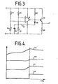
- FIG. 4 shows the charging characteristics, for example of a nickel-cadmium battery, which should preferably be charged with a constant or almost constant charging current.
- 4 shows the cell voltage (curve 4a), the cell temperature (curve 4b) and the internal gas pressure (curve 4c) of a nickel-cadmium battery over the charging time t. It should be taken into account that both the cell voltage and the cell temperature and the internal gas pressure during the charging process can vary depending on the charging current and the ambient temperature.
- the amplitudes of curves 4a, 4b and 4c can also change when the battery ages, but the curve shape, ie above all the pronounced maximum, is retained.
- the cell voltage shows a short pronounced maximum when the full charge is reached and then drops to a value which is higher than the value before the full charge was reached.
- This pronounced maximum is used in the circuit arrangement according to FIG. 2, which in the actual sense is to be regarded as a peak voltage meter and, according to curve 4d, topples over when the maximum is reached, since with falling voltage at the positive input of the comparator 71 the voltage present at the charged third capacitor 73 predominates and thus can swing the comparator output.
- the exemplary embodiment of the switching device 7 shown in FIG. 3 shows a self-holding thermal switch which uses the course of the cell temperature of a battery when the fully charged state is reached.
- first voltage divider connected in parallel with the second capacitor 12, which consists of a first voltage divider resistor 81 and a temperature-dependent resistor 84, which is thermally connected to the battery 61, and a second, likewise parallel to the second capacitor 12 connected voltage divider, which consists of the series connection of a second voltage divider resistor 82 and a third voltage divider resistor 83.
- the first voltage divider resistor is connected to the negative input of a comparator 80, while the second voltage divider is connected to the% positive input of the comparator 80.
- the output of the comparator 80 is connected via a diode 88 and a resistor 85 to the positive input of the comparator 80 bound, a capacitor 86 being connected in parallel with the third voltage divider resistor 83.
- the output of the comparator 80 is connected to the base of a transistor 89, the collector of which forms the connection terminal A according to FIG. 1, while the emitter forms the connection terminal C according to FIG. 1.
- the emitter of transistor 89 is connected to ground or reference potential via a resistor 90 and thus forms the connection terminal B according to FIG. 1.
- a further resistor 87 is connected in parallel with the base-collector path of transistor 89.
- the self-holding thermal switch shown in Fig. 3 is designed so that the output of the comparator jumps to a high voltage level when a predetermined cell temperature is exceeded, ensuring that a low tolerance of the switching temperature is achieved without adjustment. If the comparator 80 is connected to the operating voltage, the voltage at the non-inverting input of the comparator 80 is lower than that of the inverting input of the comparator until the second capacitor 12 is charged. The output of the comparator thus tilts into a position with a low voltage level.
- the output of the comparator 80 remains at a low voltage level as long as the resistance value of the temperature-dependent resistor 84 is greater than the resistance value of the third voltage divider resistor 83.
- the comparator output tilts into one position high voltage level, as a result of which the series connection of the resistor 85 with the diode 88 is connected in parallel to the second voltage divider resistor 82 and the output of the comparator 80 remains at a high voltage level for as long as the temperature-dependent resistor 84 is required in order to become more high-resistance again due to the cooling.
- This ensures that the cell temperature shown in curve 4b of FIG. 4 over the charging time with a small tolerance of the switching temperature and without adjustment of the electronic switching power supply is exactly taken into account and leads to a corresponding switchover of the electronic switching power supply when the temperature jumps at the time of full charge.
- the flyback converter oscillates unaffected by the output voltage or the output current when the base of the transistor 2 is connected to the terminal B via the decoupling diode 33, that is to say Reference potential is. If the forward voltages of the diodes 31 and 32 are neglected, the voltage across the capacitor 12 is equal to the terminal voltage of the accumulator 61. If the base of the transistor 2 is connected to the positive pole of the capacitor 12 (terminal A) via the decoupling diode 33, the transistor 2 becomes conductive and thus the flyback converter is put out of operation. The voltage across the capacitor 12 and the base voltage of the transistor 2, which is proportional to this, then decreases in accordance with its discharge time constant. If the base voltage falls below the value at which transistor 2 conducts, it is blocked and the flyback converter starts to work again. The voltage across the capacitor 12 consequently rises until the transistor 2 conducts again and puts the flyback converter out of operation again.
- the arithmetic mean of the base voltage of transistor 2 is equal to the base-emitter voltage at which this transistor conducts (approx. 0.6 V).
- the arithmetic mean of the voltage across capacitor 12 is proportional to the base voltage. Since the discharge time constant of the capacitor 12 is large, there are correspondingly large pauses between the individual charge current pulses of this capacitor, so that the arithmetic mean of this current and the charge current of the accumulator 61 is very small. The pulse-pause ratio of the battery charging current is therefore corresponding to that of the capacitor charging current.
- the switching device 7 Since the switching device 7, which is generally an electronic switch and requires an operating voltage, receives this operating voltage from the capacitor 12 and not from the battery 61, it only functions when the switched-mode power supply is connected to the supply voltage. If the switching power supply is disconnected from the supply voltage, the voltage across the capacitor 12 becomes zero. There is no galvanic connection between the switching device 7 and the accumulator 61, which is why the accumulator cannot be discharged either.
- the switching device 7 can thus be designed so that it switches the switching power supply from a high fast charging current to a low trickle charging current and vice versa depending on the cell voltage, the cell temperature or the internal gas pressure of the battery.
Abstract
Description
Gegenstand der Erfindung ist ein elektronisches Schaltnetzteil zum Laden einer Batterie bzw. eines Akkumulators aus einer Wechsel- oder Gleichspannungsquelle unterschiedlicher Spannungshöhe mit einem primär getakteten Sperrwandler, bei dem die Primärwicklung eines Ubertragers in Reihe zu einem ersten Transistor und dessen Sekundärwicklung in Reihe zur Batterie und einer ersten Diode geschaltet ist, wobei die Basis des ersten Transistors sowohl über die Reihenschaltung eines ersten Kondensators und eines ersten Widerstandes mit dem einen Wicklungsende der Sekundärwicklung des Ubertragers, deren anderes Wicklungsende an die Batterie angeschlossen ist, als auch über einen zweiten Widerstand mit dem einen Pol der Eingangsspannungsquelle und mit dem Kollektor eines zweiten Transistors verbunden ist, dessen Emitter an Bezugspotential angeschlossen ist, und wobei der Emitter des ersten Transistors sowohl über einen dritten Widerstand mit Bezugspotential als auch über eine Zenerdiode an die Basis des zweiten Transistors angeschlossen ist, die über einen vierten Widerstand mit Bezugspotential verbunden ist.The invention relates to an electronic switching power supply for charging a battery or an accumulator from an AC or DC voltage source of different voltage levels with a primary clocked flyback converter, in which the primary winding of a transformer in series with a first transistor and its secondary winding in series with the battery and one is connected to the first diode, the base of the first transistor being connected via the series connection of a first capacitor and a first resistor to one winding end of the secondary winding of the transmitter, the other winding end of which is connected to the battery, and also via a second resistor having one pole the input voltage source and is connected to the collector of a second transistor whose emitter is connected to reference potential, and wherein the emitter of the first transistor is connected to the Ba both via a third resistor with reference potential and via a Zener diode sis of the second transistor is connected, which is connected via a fourth resistor to reference potential.
Ein elektronisches Schaltnetzteil der genannten Art ist aus der DE-OS 32 18 594 bekannt, das zum Schnelladen und Erhaltungsladen einer Batterie, vorzugsweise einer Nickel-Cadmium-Batterie, dient, wobei das elektronische Schaltnetzteil grundsätzlich zur Konstantspannungs- und/oder Konstantstromversorgung elektrischer oder elektronischer Geräte vorgesehen und als primär getakteter Sperrwandler aufgebaut ist. Bei dem bekannten primär getakteten Sperrwandler ist die Primärwicklung eines Ubertragers in Reihe zu einem Schalttransistor und die Sekundärwicklung des Ubertragers in Reihe zu einem elektrischen Verbraucher in Form der Parallelschaltung einer Batterie und eines Elektromotors und einer Diode geschaltet. Darüber hinaus enthält das bekannte elektronische Schaltnetzteil einen Spannungskomparator, der aus zwei Transistoren einschließlich der zugehörigen Beschaltung besteht und den eingestellten Spannungssollwert am Verbraucher überwacht und bei Erreichen dieses Sollwertes den Schalttransistor des Sperrwand- lers sperrt. Dadurch wird der bei entsprechend entladener Batterie fließende hohe Schnelladestrom bei Erreichen des am Spannungskomparator eingestellten Spannungswertes auf einen geringen Erhaltungsladestrom für die Batterie reduziert. Die Messung der Batteriespannung erfolgt dabei nicht während des hohen in die Batterie hineinfließenden Schnelladestromes, sondern lediglich bei geringer Belastung, wodurch die infolge des Innenwiderstandes der Batterie unvermeidlichen Messfehler vermieden bzw. verringert werden. Die für die Umschaltung vom Schnelladebetrieb auf den Erhaltungsladebetrieb erforderliche Spannungsreferenzschaltung erfordert jedoch einen genauen Abgleich, um nicht durch zu spätes Umschalten die Batterie zu gefährden. Andererseits ist jedoch ein sicheres Erreichen der Volladung der Batterie zur Erhöhung der Batterielebensdauer erforderlich. Der exakte Abgleich ist jedoch auch vom Alter der Batterie und der damit verbundenen Änderung der Ladecharakteristiken der Batterie abhängig, so daß theoretisch ein ständiges Nachjustieren erforderlich ist.An electronic switching power supply of the type mentioned is known from DE-OS 32 18 594, which is used for quick charging and trickle charging of a battery, preferably a nickel-cadmium battery, the electronic switching power supply basically for constant voltage and / or constant current supply of electrical or electronic Devices provided and is constructed as a primary clocked flyback converter. In the known primary clocked flyback converter, the primary winding of a transformer is in series a switching transistor and the secondary winding of the transmitter in series with an electrical consumer in the form of the parallel connection of a battery and an electric motor and a diode. Furthermore, the known electronic switching power supply includes a voltage comparator, which consists of two transistors including the associated wiring and monitors the set voltage setpoint at consumers and the switching transistor of the barrier wall when it reaches this setpoint - toddlers locks. As a result, the high rapid charging current flowing when the battery is correspondingly discharged is reduced to a low trickle charge current for the battery when the voltage value set on the voltage comparator is reached. The measurement of the battery voltage does not take place during the high rapid charging current flowing into the battery, but only at low loads, as a result of which the measurement errors which are inevitable due to the internal resistance of the battery are avoided or reduced. However, the voltage reference circuit required for switching from fast charging to trickle charging requires precise adjustment so that the battery is not endangered by switching too late. On the other hand, however, it is necessary to safely reach the full charge of the battery in order to increase the battery life. However, the exact adjustment is also dependent on the age of the battery and the associated change in the charging characteristics of the battery, so that theoretically a constant readjustment is necessary.
Aus der EP-A-0 030 026 ist eine Schaltungsanordnung zur geregelten Speisung eines Verbrauchers bekannt, die an verschiedenen Gleich- oder Wechselspannungen sowie an verschiedenen Wechselstromfrequenzen ohne Umschaltung betrieben werden kann. Diese bekannte Schaltungsanordnung weist einen Sperrwandler auf, der mittels zweier steuerbarer Halbleiterschalter abhängig von dem durch die Primärwicklung eines Ubertragers fließenden Strom und abhängig von der zugeführten Eingangsspannung so gesteuert wird, daß die abgegebene Ausgangsleistung nahezu konstant ist. Als Verbraucher ist die Parallelschaltung einer Batterie mit einem Gleichstrommotor vorgesehen, so daß die Schaltungsanordnung beim Netzbetrieb entweder die volle Motorleistung oder bei ausgeschaltetem Motor einen Ladestrom für die Batterie liefert. Bei ausgeschaltetem Gleichstrommotor wird eine Schnelladung der Nickel-Cadmium-Batterie mit hohem Strom vorgenommen. Um eine Beschädigung der Batterie bei der Schnelladung zu vermeiden, ist bei dieser bekannten Schaltungsanordnung ein spannungsabhängiger Schalter vorgesehen, der aus einem Transistor besteht, dessen Kollektor über einen Widerstand mit der Basis des in Reihe zum Ubertrager geschalteten Schalttransistors verbunden ist und dessen Basis-Emitter-Strecke in Reihe mit einem weiteren Widerstand und einer Zenerdiode parallel zur zu ladenden Batterie geschaltet ist. Übersteigt die Batteriespannung während des Schnelladevorganges den durch die Zenerdiode vorgegebenen Wert, so schaltet der Transistor durch und sperrt damit den in Reihe zur Primärwicklung des Ubertragers geschalteten Schalttransistor. Der jeweilige Ein- und Ausschaltzeitpunkt des Sperrwandlers hängt von den durch zwei verschiedene Widerstände fließenden Strömen ab, so daß sich aus der Differenz dieser Ströme ein Hystereseverhalten ergibt. Auf diese Weise schaltet der Sperrwandler nicht ständig zwischen einem eingeschalteten und einem ausgeschaltetem Zustand hin und her, sondern macht es erforderlich, daß die Batteriespannung jeweils um einen gewissen Betrag abgesunken sein muß, bevor der Ladestrom erneut eingeschaltet wird. Mit dem Auschalten des Sperrwandlers erlöscht jeweils auch eine im Basiskreis des zweiten Transistors angeordnete Leuchtdiode und zeigt damit das Ende des Ladevorganges an. Diese Schaltungsanordnung zum Schnelladen einer Batterie mittels eines primär getakteten Sperrwandlers weist aufgrund der erforderlichen Bereitschaftsspannung für die Steuer- und Regelelektronik einen verhältnismäßig geringen Wirkungsgrad auf und bedingt zudem bei gezogenem Netzstecker, d.h. bei reinem Batteriebetrieb, eine ständige Stromentnahme aus der Batterie zum Betrieb der Steuer- und Regelelektronik. Darüber hinaus ist der Aufwand an Bauelementen verhältnismäßig groß.From EP-A-0 030 026 a circuit arrangement for the regulated supply of a consumer is known, which can be operated at different direct or alternating voltages as well as at different alternating current frequencies without switching. This known circuit arrangement has a flyback converter which is controlled by means of two controllable semiconductor switches as a function of the current flowing through the primary winding of a transmitter and as a function of the input voltage supplied in such a way that the output power output is almost constant. The parallel connection of a battery with a direct current motor is provided as the consumer, so that the circuit arrangement supplies either the full motor power during mains operation or a charging current for the battery when the motor is switched off. When the DC motor is switched off, the nickel-cadmium battery is charged quickly with high current. In order to avoid damage to the battery during rapid charging, a voltage-dependent switch is provided in this known circuit arrangement, which consists of a transistor, the collector of which is connected via a resistor to the base of the switching transistor connected in series with the transmitter and the base-emitter Route is connected in series with another resistor and a Zener diode in parallel to the battery to be charged. If the battery voltage exceeds the value specified by the zener diode during the rapid charging process, the transistor switches through and thus blocks the switching transistor connected in series with the primary winding of the transmitter. The respective switch-on and switch-off times of the flyback converter depend on the currents flowing through two different resistors, so that a hysteresis behavior results from the difference between these currents. In this way, the flyback converter does not constantly switch back and forth between an switched-on and a switched-off state, but instead requires that the battery voltage must have decreased by a certain amount before the charging current is switched on again. When the flyback converter is switched off, a light-emitting diode arranged in the base circuit of the second transistor also goes out and thus indicates the end of the charging process. This circuit arrangement for fast charging a battery by means of a primary clocked flyback converter has a relatively low efficiency owing to the required standby voltage for the control and regulating electronics and, moreover, requires a constant current draw from the battery for operating the control when the mains plug is pulled, ie when the battery is operated purely. and control electronics. In addition, the expenditure on components is relatively large.
Aufgabe der vorliegenden Erfindung ist es, ein elektronisches Schaltnetzteil zum Laden einer Batterie aus einer Wechsel- oder Gleichspannungsquelle unterschiedlicher Spannungshöhe zu schaffen, das den Ladestrom praktisch verlustfrei ein- und ausschaltet und keine Energie verbraucht, wenn es nicht an die Versorgungsspannung angeschlossen ist.The object of the present invention is to provide an electronic switching power supply for charging a battery from an AC or DC voltage source of different voltage levels, which switches the charging current on and off practically without loss and does not consume any energy when it is not connected to the supply voltage.
Diese Aufgabe wird erfindungsgemäß dadurch gelöst, daß parallel zur Sekundärwicklung des Ubertragers die Reihenschaltung eines zweiten Kondensators und einer Gleichrichtungseinrichtung vorgesehen ist, deren Verbindung an Bezugspotential angeschlossen ist, und daß parallel zum zweiten Kondensator eine Schalteinrichtung vorgesehen ist, die entweder den mit der Sekundärwicklung des Ubertragers verbundenen Anschluß des zweiten Kondensators oder den mit Bezugspotential verbundenen Anschluß des zweiten Kondensators über eine Entkopplungseinrichtung mit der Basis des zweiten Transistors verbindet.This object is achieved in that the series connection of a second capacitor and a rectifying device is provided in parallel to the secondary winding of the transmitter, the connection of which is connected to the reference potential, and in that a switching device is provided in parallel with the second capacitor, which either connects to the secondary winding of the transmitter Connected connection of the second capacitor or the connection of the second capacitor connected to reference potential via a decoupling device with the base of the second transistor.
Die erfindungsgemäße Lösung stellt sicher, daß bei ausgeschaltetem Schaltnetzteil keine Energie verbraucht wird, da die Batterie von der Schalteinrichtung getrennt ist und diese deshalb nicht entladen werden kann.The solution according to the invention ensures that no energy is consumed when the switched-mode power supply is switched off, since the battery is disconnected from the switching device and therefore cannot be discharged.
Eine vorteilhafte Ausgestaltung der erfindungsgemäßen Lösung besteht darin, daß die Schalteinrichtung bei ausgeschaltetem Schaltnetzteil die Entkopplungseinrichtung mit Bezugspotential verbindet. Dadurch ist gewährleistet, daß nach dem Einschalten des Schaltnetzteils der Sperrwandler sofort kontinuierlich schwingt und ein großer Ladestrom fließt.An advantageous embodiment of the solution according to the invention is that the switching device connects the decoupling device to the reference potential when the switched-mode power supply is switched off. This ensures that after the switching power supply is switched on, the flyback converter immediately vibrates continuously and a large charging current flows.
Eine weitere vorteilhafte Ausgestaltung ist dadurch gekennzeichnet, daß die Schalteinrichtung aus einem Hilfsspannungskreis besteht, der von der Batteriespannung beaufschlagt ist und in Abhängigkeit von den Ladecharakteristiken der Batterie bei Erreichen des Volladezustandes der Batterie umschaltet.A further advantageous embodiment is characterized in that the switching device consists of an auxiliary voltage circuit which is acted upon by the battery voltage and which switches over as a function of the charging characteristics of the battery when the battery is fully charged.
Diese Ausgestaltung ermöglicht ein Erreichen der Volladung einer Batterie, beispielsweise einer Nickel-Cadmium-Batterie, mit konstantem Ladestrom unabhängig vom Alter der Batterie und Änderungen der Ladecharakteristiken der Batterie.This configuration enables the full charge of a battery, for example a nickel-cadmium battery, to be reached with a constant charging current irrespective of the age of the battery and changes in the charging characteristics of the battery.
Eine nächste vorteilhafte Weiterbildung der Erfindung besteht darin, daß die Schalteinrichtung aus einem selbsthaltenden Thermoschalter besteht, der von der Zellentemperatur der Batterie beeinflußt ist und in Abhängigkeit von den Ladecharakteristiken der Batterie bei Erreichen des Volladezustandes der Batterie umschaltet.A next advantageous development of the invention is that the switching device consists of a self-holding thermal switch, which is influenced by the cell temperature of the battery and switches depending on the charging characteristics of the battery when the battery is fully charged.
Diese Weiterbildung bewerkstelligt ein sicheres Erreichen der Volladung der Batterie mit konstantem Ladestrom unabhängig vom Alter und von Änderungen der Ladecharakteristiken der Batterie, ohne daß äußere Einflüße, wie eventuell auftretende Spannungserhöhungen oder Spannungsspitzen, das Erreichen der Volladung beeinträchtigen. Außerdem wird ohne jeglichen Abgleich des Schaltnetzteils das Umschalten von einem hohen Schnelladestrom auf einen niedrigen Erhaltungsladestrom und umgekehrt sichergestellt.This further development ensures that the full charge of the battery is reliably reached with a constant charging current, regardless of age and changes in the charging characteristics of the battery, without external influences, such as voltage increases or voltage peaks that may occur, reaching full charge affect. In addition, switching from a high fast charging current to a low trickle charging current and vice versa is ensured without any adjustment of the switching power supply.
Weitere vorteilhafte Ausgestaltungen sind den übrigen Unteransprüchen entnehmbar.Further advantageous configurations can be found in the remaining subclaims.
Anhand von in der Zeichnung dargestellten Ausführungsbeispielen soll der der Erfindung zugrundeliegende Gedanke näher erläutert werden. Es zeigen:
- Fig. 1 ein Schaltbild eines elektronischen Schaltnetzteiles mit einer Steuer- und Regelelektronik zur Schnelladung einer Batterie mit automatischem Übergang auf eine Erhaltungsladung;
- Fig. 2 eine Prinzipschaltung einer Schalteinrichtung gemäß Fig. 1 mit einer zellenspannungsabhängigen Umschaltung;
- Fig. 3 eine Schaltung der Schalteinrichtung gemäß Fig. 1 mit zellentemperaturabhängiger Umschaltung und
- Fig. 4 eine zeitliche Darstellung der Ladecharakteristiken einer Batterie und des Umschaltvorganges.
- Figure 1 is a circuit diagram of an electronic switching power supply with control and regulating electronics for fast charging a battery with an automatic transition to a trickle charge.
- FIG. 2 shows a basic circuit of a switching device according to FIG. 1 with a cell voltage-dependent switchover;
- Fig. 3 shows a circuit of the switching device according to Fig. 1 with cell temperature-dependent switching and
- Fig. 4 is a temporal representation of the charging characteristics of a battery and the switching process.
Das in Fig. 1 dargestellte elektronische Schaltnetzteil weist einen primär getakteten Sperrwandler mit einem Ubertrager 5 und einem ersten Transistor 1 sowie einer im Lastkreis vorgesehenen ersten Diode 31 auf, die so gepolt ist, daß die in der Sperrzeit des ersten Transistors 1 im Ubertrager 5 gespeicherte Energie in die Last 6, die aus einer Batterie 61 und aus einem über einen Schalter 63 an die Batterie 61 schaltbaren Gleichstrommotor 62 besteht, entladen wird. Der Sperrwandler wird über eine Gleichrichter-Brückenschaltung 4 und einen Widerstand 28 aus einem Gleich- oder Wechselspannungsnetz gespeist, dessen Spannung zwischen 100 und 250 Volt, im Extremfall aber auch 12 Volt, und dessen Frequenz im Falle eines speisenden Wechselspannungsnetzes nahezu beliebig sein kann, variieren kann. Die gleichgerichtete Ausgangsspannung wird über eine Sieb- und Glättungsschaltung, die aus einer Längsdrossel 8 und zwei Glättungskondensatoren 91, 92 besteht, an den Eingang des Sperrwandlers bzw. der Steuer- und Regelelektronik gelegt.The electronic switching power supply shown in Fig. 1 has a primary clocked flyback converter with a
Parallel zu den Gleichspannungsklemmen ist die Reihenschaltung der Primärwicklung 51 des Ubertragers 5 mit der Kollektor-Emitter-Strecke des ersten Transistors 1 geschaltet. Die Basis des ersten Transistors 1 ist sowohl über die Reihenschaltung eines ersten Kondensators 11 und eines ersten Widerstandes 21 mit dem einen Anschluß der Sekundärwicklung 52 des Ubertragers 5 als auch über einen zweiten Widerstand 22 und die Längsdrossel 8 mit dem positiven Pol der Eingangsspannungsklemme verbunden. Darüber hinaus ist die Basis des ersten Transistors 1 über die Kollektor-Emitter-Strecke eines zweiten Transistors 2 mit Masse- oder Bezugspotential verbunden.The series connection of the
Der Emitter des ersten Transistors 1 ist an die Kathode einer ersten Zenerdiode 41 angeschlossen, deren Anode sowohl mit der Basis des zweiten Transistors 2 als auch über die Parallelschaltung eines vierten Widerstandes 24 und eines weiteren Kondensators 13 mit Masse- oder Bezugspotential verbunden ist. Darüber hinaus ist der Emitter des ersten Transistors 1 über einen dritten Widerstand 23 mit Masse- oder Bezugspotential verbunden.The emitter of the first transistor 1 is connected to the cathode of a
Der Wickelsinn der Primär- und Sekundärwicklung 51 bzw. 52 des Ubertragers 5 ist durch die eingetragenen Punkte bestimmt.The winding direction of the primary and
Parallel zur Sekundärwicklung 52 des Ubertragers 5 ist sowohl die Reihenschaltung der Batterie 61 mit der ersten Diode 31 als auch die Reihenschaltung eines zweiten Kondensators 12 mit einer zweiten Diode 32, deren Verbindung an Masse- oder Bezugspotential gelegt ist, geschaltet.Parallel to the
Der zweite Kondensator 12 ist mit den Anschlußklemmen A und B einer Schalteinrichtung 7 verbunden, deren dritte Anschlußklemme C über die Reihenschaltung eines fünften Widerstandes 25 mit einer dritten Diode 33 an die Verbindung der Anode der Zenerdiode 41 mit der Basis des zweiten Transistors 2 angeschlossen ist, wobei die Kathode der dritten Diode 33 mit der Anode der Zenerdiode 41 verbunden ist. Die Schalteinrichtung 7 ist so beschaffen, daß die dritte Anschlußklemme C entweder mit der Anschlußklemme A oder mit der Anschlußklemme B verbunden wird, wobei hier die Anschlußklemme A über eine weitere Diode 35 mit der Anschlußklemme C verbindbar ist.The second capacitor 12 is connected to the connection terminals A and B of a switching device 7, the third connection terminal C of which is connected via the series connection of a
Nachstehend soll die Funktionsweise des elektronischen Schaltnetzteiles gemäß Fig. 1 näher erläutert werden.The operation of the electronic switching power supply according to FIG. 1 will be explained in more detail below.
Nach der Gleichrichtung der am Eingang der Gleichrichter-Brückenschaltung 4 anliegenden Gleich- oder Wechselspannung und nachfolgender Siebung bzw. Glättung mittels der Längsdrossel 8 bzw. der Querkondensatoren 91, 92 wird der als Schalttransistor arbeitende erste Transistor 1 über den zweiten Widerstand 22 mit einem geringen Basisstrom angesteuert, infolgedessen der erste Transistor 1 in den leitenden Zustand gesteuert wird. Über die Schaltstrecke des ersten Transistors 1 und die Primärwicklung 51 des Ubertragers 5 entsteht ein Mitkopplungseffekt, durch den der erste Transistor 1 zusätzlich angesteuert und schlagartig in den vollständig leitenden Zustand geschaltet wird. Der Kollektorstrom steigt linear an und erzeugt am dritten Widerstand 23 eine dem jeweiligen Kollektorstrom proportionale Spannung. Beim Erreichen eines bestimmten Spitzenstromwertes des Kollektorstromes bzw. einer entsprechend proportionalen Spannung wird über die Zenerdiode 41 der zweite Transistor angesteuert, gelangt dadurch in den leitenden Zustand und verbindet die Basis des ersten Transistors 1 mit Masse- bzw. Bezugspotential und entzieht damit dem ersten Transistor 1 den Basisstrom, woraufhin der erste Transistor 1 sperrt.After rectification of the DC or AC voltage present at the input of the rectifier bridge circuit 4 and subsequent screening or smoothing by means of the series inductor 8 or the
Mit Beginn der Sperrphase des ersten Transistors 1 wechselt die Polarität der in der Sekundärwicklung 52 des Ubertragers 5 induzierten Spannung. Die im Ubertrager 5 gespeicherte Energie wird damit nach dem Prinzip des Sperrwandlers über die erste Diode 31 an die Batterie 61 abgegeben.At the beginning of the blocking phase of the first transistor 1, the polarity of the voltage induced in the
Während des Umschwingvorganges des Ubertragers 5 begrenzen die parallel zur Primärwicklung 51 des Ubertragers 5 geschaltete Reihenschaltung der Diode 34 mit der Zenerdiode 42 die Rückschaltspannungsspitze während der Sperrphase des ersten Transistors 1, wobei die Diode 34 und die Zenerdiode 42 entweder kathodenseitig oder anodenseitig zusammengeschaltet sind.During the switching process of the
Im Leitzustand des ersten Transistors 1 wird der erste Kondensator 11 über den ersten Widerstand 21 aufgeladen und im Sperrzustand des ersten Transistors 1 so umgeladen, daß an seiner mit der Basis des ersten Transistors 1 verbundenen Elektrode eine positive Spannung ansteht, die auch bei sehr niedriger Betriebsspannung von z. B. 12 Volt ein sofortiges Wiedereinschalten des ersten Transistors 1 gewährleistet, wenn nach Beendigung der Ubertrager-Entladephase der zweite Transistor 2 sperrt und somit der erste Transistor 1 in den Leitzustand gesteuert wird.In the conducting state of the first transistor 1, the first capacitor 11 is charged via the
In der in Fig. 1 dargestellten Schaltverbindung der Schalteinrichtung 7, bei der die aus Diode 33 und Widerstand 25 bestehende Entkopplungseinrichtung mit Bezugspotential verbunden ist, erfolgt ein Schnelladen der Batterie 61, wobei der Batterieladestrom durch den primärseitigen Spitzenstrom und die Induktivität des Ubertragers bestimmt wird. Die Spannung am zweiten Kondensator 12 beträgt
In der entgegengesetzten Schaltstellung der Schalteinrichtung 7 erfolgt eine Ladung der Batterie 61 mit einem Erhaltungsladestrom, wobei die Spannung am zweiten Kondensator 12
beträgt, wobei UBET2 den Basis-Emitter-Spannungsabfall am zweiten Transistor, R24 den Widerstandswert des vierten Widerstandes 24, R25 den Widerstandswert des fünften Widerstandes 25, Uf33 den Spannungsabfall an der dritten Diode 33 und Uf35 den Durchlaßspannungsabfall an der fünften Diode 35 bedeutet.In the opposite switching position of the switching device 7, the battery 61 is charged with a trickle charge current, the voltage at the second capacitor 12
is, where U BET2 the base-emitter voltage drop across the second transistor, R 24 the resistance value of the fourth resistor of the 24, R 25 the resistance value of the
Aufgrund der beiden oben stehenden Gleichungen fließt immer dann ein Ladestrom in die Batterie 61, wenn die Summe der Spannung am zweiten Kondensator 12 UCEL und Uf32 größer ist als die Summe der Spannung an der Batterie UBatt und dem Durchlaßspannungsabfall Uf31 an der ersten Diode 31. Damit ist während des Erhaltungsladezustandes der Ladestrom drastisch gegenüber dem Ladestrom im Schnelladezustand reduziert. In beiden Schaltstellungen der Schalteinrichtung 7 steht jedoch am zweiten Kondensator 12 eine Spannung zur Verfügung.Based on the two equations above, a charging current always flows into the battery 61 when the sum of the voltage at the second capacitor 12 U CEL and U f32 is greater than the sum of the voltage at the battery U Batt and the forward voltage drop U f31 at the first Diode 31. This means that the charge current is drastically reduced compared to the charge current in the fast charge state during the trickle charge state. In both switching positions of the switching device 7, however, a voltage is available on the second capacitor 12.
Während des Schwingvorganges des Sperrwandlers schaltet der erste Transistor 1 immer dann in den Leitzustand, wenn die Basisspannung des zweiten Transistors 2 unter einen bestimmten, durch die Zenerdiode 41 vorgegebenen Spannungswert abfällt, so daß während der Entladung des Ubertragers 5 der zweite Transistor 2 sperrt und damit der erste Transistor 1 über den zweiten Widerstand 22 und mit Unterstützung der entsprechend umgepolten Ladung im ersten Kondensator 11 in den Leitzustand gesteuert wird.During the oscillation process of the flyback converter, the first transistor 1 always switches to the conducting state when the base voltage of the second transistor 2 drops below a certain voltage value specified by the
Anhand der Figuren 2 und 3 sollen verschiedene Ausführungsbeispiele der Schalteinrichtung 7 zur Berücksichtigung des jeweiligen Ladezustandes der Batterie 61 näher erläutert werden.Various exemplary embodiments of the switching device 7 for taking into account the respective state of charge of the battery 61 are to be explained in more detail with reference to FIGS. 2 and 3.
0 Das in Fig. 2 dargestellte Ausführungsbeispiel zeigt eine Schalteinrichtung, die die Zellenspannung der Batterie 61 erfaßt und bei einem bestimmten Zellenspannungswert umschaltet. Sie enthält einen Differenzverstärker 71, dessen positiver Eingang mit dem oberen Pol der Batterie 61 beaufschlagt ist, während der negative Eingang über einen dritten Kondensator 73 mit dem unteren Pol der Batterie 61 sowie über eine vierte Diode 72 mit seinem Ausgang verbunden ist, wobei die Anode der vierten Diode 72 an den Ausgang des Differenzverstärkers 71 angeschlossen ist.The exemplary embodiment shown in FIG. 2 shows a switching device which detects the cell voltage of the battery 61 and switches over at a specific cell voltage value. It contains a
Der Ausgang des Differenzverstärkers 71 ist mit der Basis eines dritten Transistors 74 verbunden, dessen Kollektor an die Basis eines vierten Transistors 89 geführt ist und über einen sechsten Widerstand 75 mit dem Kollektor des vierten Transistors 89 verbunden ist und die Anschlußklemme A gemäß Fig. 1 bildet. Der Emitter des Transistors 89, der die Anschlußklemme C gemäß Fig. 1 bildet, ist über einen Widerstand 90 mit Masse- oder Bezugspotential, das die Anschlußklemme B darstellt, verbunden.The output of the
In Verbindung mit der Darstellung gemäß Fig. 4 soll die Funktionsweise der Anordnung gemäß Fig. 2 erläutert werden.The operation of the arrangement according to FIG. 2 will be explained in connection with the illustration according to FIG. 4.
Fig. 4 zeigt die Ladecharakteristiken beispielsweise einer Nickel-Cadmium-Batterie, die vorzugsweise mit konstantem oder nahezu konstantem Ladestrom geladen werden soll. Die Darstellung gemäß Fig. 4 zeigt die Zellenspannung (Kurve 4a), die Zellentemperatur (Kurve 4b) und den internen Gasdruck (Kurve 4c) einer Nickel-Cadmium-Batterie über der Ladezeit t. Dabei ist zu berücksichtigen, daß sowohl die Zellenspannung als auch die Zellentemperatur und der interne Gasdruck während des Ladevorganges in Abhängigkeit vom Ladestrom und der Umgebungstemperatur variieren können. Auch bei Alterung der Batterie können sich die Amplituden der Kurven 4a, 4b und 4c verändern, wobei jedoch die Kurvenform, d.h. vor allem das ausgeprägte Maximum, erhalten bleibt.FIG. 4 shows the charging characteristics, for example of a nickel-cadmium battery, which should preferably be charged with a constant or almost constant charging current. 4 shows the cell voltage (curve 4a), the cell temperature (
Wie der Darstellung gemäß Kurve 4a der Fig. 4 zu entnehmen ist, zeigt die Zellenspannung bei Erreichen der Volladung ein kurzes ausgeprägtes Maximum und fällt dann auf einen Wert ab, der höher ist als der Wert vor Erreichen der Volladung. Dieses ausgeprägte Maximum wird bei der Schaltungsanordnung gemäß Fig. 2 ausgenutzt, die im eigentlichen Sinne als Spitzenspannungsmesser anzusehen ist und gemäß Kurve 4d bei Erreichen des Maximums umkippt, da bei fallender Spannung am positiven Eingang des Komparators 71 die am aufgeladenen dritten Kondensator 73 anliegende Spannung überwiegt und somit den Komparatorausgang umschwingen läßt.As can be seen in the representation according to curve 4a of FIG. 4, the cell voltage shows a short pronounced maximum when the full charge is reached and then drops to a value which is higher than the value before the full charge was reached. This pronounced maximum is used in the circuit arrangement according to FIG. 2, which in the actual sense is to be regarded as a peak voltage meter and, according to curve 4d, topples over when the maximum is reached, since with falling voltage at the positive input of the
Das in Fig. 3 dargestellte Ausführungsbeispiel der Schalteinrichtung 7 zeigt einen den Verlauf der Zellentemperatur einer Batterie bei Erreichen des Volladezustandes ausnutzenden selbsthaltenden Thermoschalter.The exemplary embodiment of the switching device 7 shown in FIG. 3 shows a self-holding thermal switch which uses the course of the cell temperature of a battery when the fully charged state is reached.
Der selbsthaltende Thermoschalter gemäß Fig. 3 weist einen ersten parallel zum zweiten Kondensator 12 geschalteten Spannungsteiler, der aus einem ersten Spannungsteilerwiderstandes 81 und einem temperaturabhängigen Widerstand 84, der thermisch mit der Batterie 61 verbunden ist, besteht sowie einen zweiten, ebenfalls parallel zum zweiten Kondensator 12 geschalteten Spannungsteiler, der aus der Reihenschaltung eines zweiten Spannungsteilerwiderstandes 82 und eines dritten Spannungsteilerwiderstandes 83 besteht, auf. Der erste Spannungsteilerwiderstand ist an den negativen Eingang eines Komparators 80 angeschlossen, während der zweite Spannungsteiler an den %positiven Eingang des Komparators 80 angeschlossen ist.3 has a first voltage divider connected in parallel with the second capacitor 12, which consists of a first voltage divider resistor 81 and a temperature-
Der Ausgang des Komparators 80 ist über eine Diode 88 und einen Widerstand 85 mit dem positiven Eingang des Komparators 80 verbunden, wobei parallel zum dritten Spannungsteilerwiderstand 83 ein Kondensator 86 geschaltet ist. Darüber hinaus ist der Ausgang des Komparators 80 mit der Basis eines Transistors 89 verbunden, dessen Kollektor die Anschlußklemme A gemäß Fig. 1 bildet, während der Emitter die Anschlußklemme C gemäß Fig. 1 bildet. Über einen Widerstand 90 ist der Emitter des Transistors 89 mit Masse- oder Bezugspotential verbunden und formt damit die Anschlußklemme B gemäß Fig. 1. Parallel zur Basis-Kollektor-Strecke des Transistors 89 ist ein weiterer Widerstand 87 geschaltet.The output of the
Der in Fig. 3 dargestellte selbsthaltende Thermoschalter ist so ausgebildet, daß der Ausgang des Komparators auf einen hohen Spannungspegel bei Überschreiten einer vorgegebenen Zellentemperatur springt, wobei sichergestellt ist, daß ohne Abgleich eine geringe Toleranz der Schalttemperatur erreicht wird. Wird der Komparator 80 an Betriebsspannung gelegt, so ist die Spannung am nichtinvertierenden Eingang des Komparators 80 so lange gegenüber der des invertierenden Eingangs des Komparators niedriger bis der zweite Kondensator 12 aufgeladen ist. Damit kippt der Ausgang des Komparators in eine Stellung mit niedrigem Spannungspegel. Unter der Voraussetzung, daß der Widerstandswert des ersten Spannungsteilerwiderstandes 81 gleich dem des zweiten Spannungsteilerwiderstandes 82 ist, bleibt der Ausgang des Komparators 80 so lange auf niedrigem Spannungspegel wie der Widerstandswert des temperaturabhängigen Widerstandes 84 größer als der Widerstandswert des dritten Spannungsteilerwiderstandes 83 ist.The self-holding thermal switch shown in Fig. 3 is designed so that the output of the comparator jumps to a high voltage level when a predetermined cell temperature is exceeded, ensuring that a low tolerance of the switching temperature is achieved without adjustment. If the
Wenn bei steigender Zellentemperatur der Batterie 61 der Widerstandswert des temperaturabhängigen (NTC-) Widerstandes 84 kleiner wird als der Widerstandswert des dritten Spannungsteilerwiderstandes 83 kippt der Komparatorausgang in eine Stellung mit hohem Spannungspegel, wodurch die Reihenschaltung des Widerstandes 85 mit der Diode 88 parallel zum zweiten Spannungsteilerwiderstandes 82 geschaltet wird und der Ausgang des Komparators 80 so lange auf hohem Spannungspegel bleibt wie der temperaturabhängige Widerstand 84 benötigt, um aufgrund der Abkühlung wieder hochohmiger zu werden. Dadurch ist sichergestellt, daß die in Kurve 4b der Fig. 4 dargestellte Zellentemperatur über der Ladezeit mit geringer Toleranz der Schalttemperatur und ohne Abgleich des elektronischen Schaltnetzteiles exakt berücksichtigt wird und zu einer entsprechenden Umschaltung des elektronischen Schaltnetzteiles beim Temperatursprung zum Zeitpunkt der Volladung führt.If, as the cell temperature of the battery 61 increases, the resistance value of the temperature-dependent (NTC)
Zusammenfassend gilt also also für die Wirkungsweise der in Fig. 1, 2 und 3 gezeigten Schaltungsanordnungen, daß der Sperrwandler unbeeinflußt von der Ausgangsspannung bzw. dem Ausgangsstrom schwingt, wenn die Basis des Transistors 2 über die Entkopplungsdiode 33 an der Anschlußklemme B, das heißt an Bezugspotential liegt. Die am Kondensator 12 anliegende Spannung ist bei Vernachlässigung der Durchlaßspannungen der Dioden 31 und 32 gleich der Klemmenspannung des Akkumulators 61. Wenn die Basis des Transistors 2 über die Entkopplungsdiode 33 am positiven Pol des Kondensators 12 (Anschlußklemme A) liegt, wird der Transistor 2 leitend und damit der Sperrwandler außer Betrieb gesetzt. Die Spannung am Kondensator 12 und dazu proportional die Basisspannung des Transistors 2 sinkt damit dann entsprechend seiner Entladezeitkonstante ab. Wenn die Basisspannung den Wert unterschreitet, bei dem der Transistor 2 leitet, wird dieser gesperrt und der Sperrwandler beginnt wieder zu arbeiten. Die Spannung am Kondensator 12 steigt infolgedessen an bis der Transistor 2 wieder leitet und den Sperrwandler erneut außer Betrieb setzt.In summary, therefore, for the mode of operation of the circuit arrangements shown in FIGS. 1, 2 and 3, the flyback converter oscillates unaffected by the output voltage or the output current when the base of the transistor 2 is connected to the terminal B via the
Dieser Vorgang wiederholt sich laufend. Der arithmetische Mittelwert der Basisspannung des Transistors 2 ist gleich der Basis-Emitter-Spannung bei der dieser Transistor leitet (ca. 0,6V). Der arithmetische Mittelwert der Spannung am Kondensator 12 ist der Basisspannung proportional. Da die Entladezeitkonstante des Kondensators 12 groß ist, sind zwischen den einzelnen Ladestromimpulsen dieses Kondensators entsprechend große Pausen, so daß der arithmetische Mittelwert dieses Stromes und des Ladestromes des Akkumulators 61 sehr klein ist. Das Puls-Pausen-Verhältnis des Akkumulatorladestromes ist also entsprechend dem des Kondensatorladestromes.This process is repeated continuously. The arithmetic mean of the base voltage of transistor 2 is equal to the base-emitter voltage at which this transistor conducts (approx. 0.6 V). The arithmetic mean of the voltage across capacitor 12 is proportional to the base voltage. Since the discharge time constant of the capacitor 12 is large, there are correspondingly large pauses between the individual charge current pulses of this capacitor, so that the arithmetic mean of this current and the charge current of the accumulator 61 is very small. The pulse-pause ratio of the battery charging current is therefore corresponding to that of the capacitor charging current.
Da die Schalteinrichtung 7, die im allgemeinen ein elektronischer Schalter ist und eine Betriebsspannung benötigt, diese Betriebsspannung vom Kondensator 12 und nicht etwa von der Batterie 61 erhält, ist er nur in Funktion, wenn das Schaltnetzteil mit der Versorgungsspannung verbunden ist. Wird das Schaltnetzteil von der Versorgungsspannung getrennt, wird die Spannung am Kondensator 12 Null. Eine galvanische Verbindung zwischen Schalteinrichtung 7 und Akkumulator 61 besteht nicht, weshalb der Akkumulator auch nicht entladen werden kann.Since the switching device 7, which is generally an electronic switch and requires an operating voltage, receives this operating voltage from the capacitor 12 and not from the battery 61, it only functions when the switched-mode power supply is connected to the supply voltage. If the switching power supply is disconnected from the supply voltage, the voltage across the capacitor 12 becomes zero. There is no galvanic connection between the switching device 7 and the accumulator 61, which is why the accumulator cannot be discharged either.
Es wird also keine Energie durch die Schalteinrichtung 7 verbraucht, wenn das Schaltnetzteil nicht an die Versorgungsspannung angeschlossen ist und es erfolgt ein verlustloses Schalten des Ausgangsstroms des Sperrwandlers.No energy is therefore consumed by the switching device 7 when the switched-mode power supply is not connected to the supply voltage and the output current of the flyback converter is switched without loss.
In analoger Weise sind auch andere Schalteinrichtungen 7, die die Ladecharakteristiken wie beispielsweise den in Kurve 4c der Fig. 4 dargestellten Verlauf des Zellendruckes einer Batterie berücksichtigen, herstellbar und für das in Fig. 1 dargestellte elektronische Schaltnetzteil verwendbar.In an analogous manner, other switching devices 7, which take into account the charging characteristics such as, for example, the curve of the cell pressure of a battery shown in curve 4c in FIG. 4, can be produced and used for the electronic switching power supply shown in FIG. 1.
Die Schalteinrichtung 7 kann also so ausgestaltet werden, daß sie in Abhängigkeit von der Zellenspannung, der Zellentemperatur oder dem inneren Gasdruck der Batterie das Schaltnetzteil von einem hohen Schnelladestrom auf einen niedrigen Erhaltungsladestrom und umgekehrt umschaltet.The switching device 7 can thus be designed so that it switches the switching power supply from a high fast charging current to a low trickle charging current and vice versa depending on the cell voltage, the cell temperature or the internal gas pressure of the battery.
Claims (8)
Priority Applications (1)
| Application Number | Priority Date | Filing Date | Title |
|---|---|---|---|
| AT86116807T ATE43209T1 (en) | 1985-12-20 | 1986-12-03 | ELECTRONIC SWITCHING POWER SUPPLY. |
Applications Claiming Priority (2)
| Application Number | Priority Date | Filing Date | Title |
|---|---|---|---|
| DE3545324 | 1985-12-20 | ||
| DE19853545324 DE3545324A1 (en) | 1985-12-20 | 1985-12-20 | ELECTRONIC SWITCHING POWER SUPPLY |
Publications (4)
| Publication Number | Publication Date |
|---|---|
| EP0226128A2 true EP0226128A2 (en) | 1987-06-24 |
| EP0226128A3 EP0226128A3 (en) | 1988-08-31 |
| EP0226128B1 EP0226128B1 (en) | 1989-05-17 |
| EP0226128B2 EP0226128B2 (en) | 1994-05-11 |
Family
ID=6289100
Family Applications (1)
| Application Number | Title | Priority Date | Filing Date |
|---|---|---|---|
| EP86116807A Expired - Lifetime EP0226128B2 (en) | 1985-12-20 | 1986-12-03 | Electronic switching power supply |
Country Status (4)
| Country | Link |
|---|---|
| US (1) | US4706009A (en) |
| EP (1) | EP0226128B2 (en) |
| AT (1) | ATE43209T1 (en) |
| DE (2) | DE3545324A1 (en) |
Cited By (6)
| Publication number | Priority date | Publication date | Assignee | Title |
|---|---|---|---|---|
| WO1989007854A1 (en) * | 1988-02-09 | 1989-08-24 | Braun Aktiengesellschaft | Process and circuit arrangement for determining the charging time of an accumulator |
| EP0383381A1 (en) * | 1989-02-14 | 1990-08-22 | Koninklijke Philips Electronics N.V. | Power supply circuit |
| EP0548749A1 (en) * | 1991-12-24 | 1993-06-30 | FIAT AUTO S.p.A. | Electronic circuit for direct-current feed to electrical loads, particularly storage batteries for electric vehicles |
| WO1995012840A1 (en) * | 1993-11-03 | 1995-05-11 | Braun Aktiengesellschaft | Switched-mode power supply |
| WO1995013645A1 (en) * | 1993-11-09 | 1995-05-18 | Braun Aktiengesellschaft | Circuit for controlling a charging current circuit for a storage cell |
| CN108695953A (en) * | 2017-04-05 | 2018-10-23 | 赛米控电子股份有限公司 | Power converter arrangement for powering to vehicle and the equipment including the device |
Families Citing this family (10)
| Publication number | Priority date | Publication date | Assignee | Title |
|---|---|---|---|---|
| US5266881A (en) * | 1989-04-11 | 1993-11-30 | Solid State Chargers Research And Development Limited | Universal high current battery charger |
| DE4008663C1 (en) * | 1990-03-17 | 1991-05-02 | Braun Ag, 6000 Frankfurt, De | |
| DE4122544C1 (en) * | 1991-07-08 | 1992-07-16 | Braun Ag, 6000 Frankfurt, De | |
| JP2500580B2 (en) * | 1992-01-30 | 1996-05-29 | 日本電気株式会社 | Power supply circuit |
| FR2956261B1 (en) * | 2010-02-05 | 2012-03-09 | Commissariat Energie Atomique | BALANCING SYSTEM FOR BATTERIES OF ACCUMULATORS |
| EP2532068B1 (en) | 2010-02-05 | 2014-08-13 | Commissariat à l'Énergie Atomique et aux Énergies Alternatives | Charge equalization system for batteries |
| CN102735906B (en) | 2012-07-05 | 2014-11-05 | 矽力杰半导体技术(杭州)有限公司 | Inductive current detecting circuit and LED (light emitting diode) driving circuit using inductive current detecting circuit |
| KR102048795B1 (en) * | 2012-08-30 | 2019-11-26 | 휴렛-팩커드 디벨롭먼트 컴퍼니, 엘.피. | Discharging circuit, image forming apparatus having discharging circuit and power supplying unit |
| US9513318B2 (en) * | 2014-05-29 | 2016-12-06 | Infineon Technologies Ag | Current or voltage sensing |
| JP2019193324A (en) * | 2018-04-18 | 2019-10-31 | オンキヨー株式会社 | Switching power supply |
Citations (2)
| Publication number | Priority date | Publication date | Assignee | Title |
|---|---|---|---|---|
| EP0030026A1 (en) * | 1979-11-29 | 1981-06-10 | Klaus Becker | Circuit arrangement for the regular supply to a user |
| EP0056593A1 (en) * | 1981-01-17 | 1982-07-28 | Braun Aktiengesellschaft | Switching device for regulating the supply of a consumer apparatus |
Family Cites Families (8)
| Publication number | Priority date | Publication date | Assignee | Title |
|---|---|---|---|---|
| US3895283A (en) * | 1973-11-26 | 1975-07-15 | Vapor Corp | Temperature responsive battery charging circuit |
| US4220909A (en) * | 1976-05-13 | 1980-09-02 | R. E. Phelon Company | Half-wave regulator rectifier for an alternator |
| US4464619A (en) * | 1981-02-05 | 1984-08-07 | Braun Aktiengesellschaft | Circuit arrangement for the controlled supply to a load |
| DE3218594A1 (en) * | 1982-05-17 | 1983-12-22 | Braun Ag, 6000 Frankfurt | ELECTRONIC SWITCHING POWER SUPPLY |
| JPS5925533A (en) * | 1982-07-31 | 1984-02-09 | 松下電工株式会社 | Quick charging circuit |
| SE451924B (en) * | 1982-10-12 | 1987-11-02 | Ericsson Telefon Ab L M | REGULATOR FOR REGULATING A CHARGING CURRENT TO A SINGLE CELL IN A BATTERY OF CELLS |
| DE3311737C2 (en) * | 1983-03-31 | 1986-10-16 | Braun Ag, 6000 Frankfurt | Electronic switching power supply |
| DE3323747A1 (en) * | 1983-07-01 | 1985-01-03 | Braun Ag, 6000 Frankfurt | ELECTRONIC SWITCHING POWER SUPPLY |
-
1985
- 1985-12-20 DE DE19853545324 patent/DE3545324A1/en not_active Withdrawn
-
1986
- 1986-12-03 EP EP86116807A patent/EP0226128B2/en not_active Expired - Lifetime
- 1986-12-03 AT AT86116807T patent/ATE43209T1/en not_active IP Right Cessation
- 1986-12-03 DE DE8686116807T patent/DE3663430D1/en not_active Expired
- 1986-12-15 US US06/941,920 patent/US4706009A/en not_active Expired - Fee Related
Patent Citations (2)
| Publication number | Priority date | Publication date | Assignee | Title |
|---|---|---|---|---|
| EP0030026A1 (en) * | 1979-11-29 | 1981-06-10 | Klaus Becker | Circuit arrangement for the regular supply to a user |
| EP0056593A1 (en) * | 1981-01-17 | 1982-07-28 | Braun Aktiengesellschaft | Switching device for regulating the supply of a consumer apparatus |
Cited By (7)
| Publication number | Priority date | Publication date | Assignee | Title |
|---|---|---|---|---|
| WO1989007854A1 (en) * | 1988-02-09 | 1989-08-24 | Braun Aktiengesellschaft | Process and circuit arrangement for determining the charging time of an accumulator |
| EP0383381A1 (en) * | 1989-02-14 | 1990-08-22 | Koninklijke Philips Electronics N.V. | Power supply circuit |
| EP0548749A1 (en) * | 1991-12-24 | 1993-06-30 | FIAT AUTO S.p.A. | Electronic circuit for direct-current feed to electrical loads, particularly storage batteries for electric vehicles |
| WO1995012840A1 (en) * | 1993-11-03 | 1995-05-11 | Braun Aktiengesellschaft | Switched-mode power supply |
| US5708572A (en) * | 1993-11-03 | 1998-01-13 | Braun Aktiengesellschaft | Switched-mode power supply |
| WO1995013645A1 (en) * | 1993-11-09 | 1995-05-18 | Braun Aktiengesellschaft | Circuit for controlling a charging current circuit for a storage cell |
| CN108695953A (en) * | 2017-04-05 | 2018-10-23 | 赛米控电子股份有限公司 | Power converter arrangement for powering to vehicle and the equipment including the device |
Also Published As
| Publication number | Publication date |
|---|---|
| EP0226128B2 (en) | 1994-05-11 |
| DE3545324A1 (en) | 1987-06-25 |
| ATE43209T1 (en) | 1989-06-15 |
| US4706009A (en) | 1987-11-10 |
| EP0226128B1 (en) | 1989-05-17 |
| EP0226128A3 (en) | 1988-08-31 |
| DE3663430D1 (en) | 1989-06-22 |
Similar Documents
| Publication | Publication Date | Title |
|---|---|---|
| EP0162341B1 (en) | Electronic switching power supply | |
| EP0226128B2 (en) | Electronic switching power supply | |
| DE3310678C2 (en) | Circuit for regulating the output voltage of an electronic switched-mode power supply | |
| DE3101375C2 (en) | Circuit arrangement for the regulated supply of a consumer | |
| DE3923919C2 (en) | Electrical supply source | |
| EP0057910B2 (en) | Circuit for the regulated supply to a user | |
| DE2838009C2 (en) | Current limiting circuit for a direct current converter | |
| EP0593518B1 (en) | Electronic power supply unit | |
| EP0030276A1 (en) | Circuit arrangement for charging a battery | |
| DE3221404A1 (en) | POWER SUPPLY CIRCUIT | |
| DE2402182B2 (en) | Battery charger | |
| EP0152913B1 (en) | Circuit arrangement for a flyback converter | |
| WO1995012840A1 (en) | Switched-mode power supply | |
| DE3103863C2 (en) | Circuit arrangement for supplying a direct current consumer with constant current from input direct voltage sources of different voltages | |
| EP0635171B1 (en) | Switched electronic supply unit | |
| EP0475296B1 (en) | Switching power supply device with a forward- and a flyback-converter output | |
| EP0320605B1 (en) | Electronic switching power supply with an inductance dc-dc converter | |
| DE3311737C2 (en) | Electronic switching power supply | |
| EP0130411A2 (en) | Electronic switching power supply | |
| DE3300285C2 (en) | Electronic switching power supply | |
| EP0400041B1 (en) | Process and circuit arrangement for determining the charging time of an accumulator | |
| DE3334732A1 (en) | Electronic switched-mode power supply having a reactor converter | |
| DE3210269A1 (en) | Controllable DC converter | |
| CH665506A5 (en) | CIRCUIT ARRANGEMENT FOR OPERATING A LOAD. | |
| DD251656A1 (en) | CONTROLLED DC VOLTAGE FLOW CONVERTER FOR DEFINED CHARGING AND DISCHARGE OF ACCUMULATOR CELLS |
Legal Events
| Date | Code | Title | Description |
|---|---|---|---|
| PUAI | Public reference made under article 153(3) epc to a published international application that has entered the european phase |
Free format text: ORIGINAL CODE: 0009012 |
|
| AK | Designated contracting states |
Kind code of ref document: A2 Designated state(s): AT CH DE FR GB LI NL |
|
| PUAL | Search report despatched |
Free format text: ORIGINAL CODE: 0009013 |
|
| AK | Designated contracting states |
Kind code of ref document: A3 Designated state(s): AT CH DE FR GB LI NL |
|
| 17P | Request for examination filed |
Effective date: 19880723 |
|
| 17Q | First examination report despatched |
Effective date: 19881102 |
|
| GRAA | (expected) grant |
Free format text: ORIGINAL CODE: 0009210 |
|
| AK | Designated contracting states |
Kind code of ref document: B1 Designated state(s): AT CH DE FR GB LI NL |
|
| REF | Corresponds to: |
Ref document number: 43209 Country of ref document: AT Date of ref document: 19890615 Kind code of ref document: T |
|
| GBT | Gb: translation of ep patent filed (gb section 77(6)(a)/1977) | ||
| REF | Corresponds to: |
Ref document number: 3663430 Country of ref document: DE Date of ref document: 19890622 |
|
| ET | Fr: translation filed | ||
| PLBI | Opposition filed |
Free format text: ORIGINAL CODE: 0009260 |
|
| 26 | Opposition filed |
Opponent name: N.V. PHILIPS' GLOEILAMPENFABRIEKEN Effective date: 19900215 |
|
| NLR1 | Nl: opposition has been filed with the epo |
Opponent name: N.V. PHILIPS' GLOEILAMPENFABRIEKEN |
|
| PGFP | Annual fee paid to national office [announced via postgrant information from national office to epo] |
Ref country code: GB Payment date: 19911121 Year of fee payment: 6 |
|
| PGFP | Annual fee paid to national office [announced via postgrant information from national office to epo] |
Ref country code: FR Payment date: 19911127 Year of fee payment: 6 |
|
| PGFP | Annual fee paid to national office [announced via postgrant information from national office to epo] |
Ref country code: CH Payment date: 19920212 Year of fee payment: 6 |
|
| PG25 | Lapsed in a contracting state [announced via postgrant information from national office to epo] |
Ref country code: GB Effective date: 19921203 |
|
| PG25 | Lapsed in a contracting state [announced via postgrant information from national office to epo] |
Ref country code: LI Effective date: 19921231 Ref country code: CH Effective date: 19921231 |
|
| GBPC | Gb: european patent ceased through non-payment of renewal fee |
Effective date: 19921203 |
|
| PG25 | Lapsed in a contracting state [announced via postgrant information from national office to epo] |
Ref country code: FR Effective date: 19930831 |
|
| REG | Reference to a national code |
Ref country code: CH Ref legal event code: PL |
|
| REG | Reference to a national code |
Ref country code: FR Ref legal event code: ST |
|
| PGFP | Annual fee paid to national office [announced via postgrant information from national office to epo] |
Ref country code: AT Payment date: 19931202 Year of fee payment: 8 |
|
| PGFP | Annual fee paid to national office [announced via postgrant information from national office to epo] |
Ref country code: DE Payment date: 19931208 Year of fee payment: 8 |
|
| PGFP | Annual fee paid to national office [announced via postgrant information from national office to epo] |
Ref country code: NL Payment date: 19931231 Year of fee payment: 8 |
|
| PUAH | Patent maintained in amended form |
Free format text: ORIGINAL CODE: 0009272 |
|
| STAA | Information on the status of an ep patent application or granted ep patent |
Free format text: STATUS: PATENT MAINTAINED AS AMENDED |
|
| 27A | Patent maintained in amended form |
Effective date: 19940511 |
|
| AK | Designated contracting states |
Kind code of ref document: B2 Designated state(s): AT CH DE FR GB LI NL |
|
| NLR2 | Nl: decision of opposition | ||
| NLR3 | Nl: receipt of modified translations in the netherlands language after an opposition procedure | ||
| EN3 | Fr: translation not filed ** decision concerning opposition | ||
| PG25 | Lapsed in a contracting state [announced via postgrant information from national office to epo] |
Ref country code: AT Effective date: 19941203 |
|
| PG25 | Lapsed in a contracting state [announced via postgrant information from national office to epo] |
Ref country code: NL Effective date: 19950701 |
|
| NLV4 | Nl: lapsed or anulled due to non-payment of the annual fee |
Effective date: 19950701 |
|
| PG25 | Lapsed in a contracting state [announced via postgrant information from national office to epo] |
Ref country code: DE Effective date: 19950901 |
|
| APAH | Appeal reference modified |
Free format text: ORIGINAL CODE: EPIDOSCREFNO |