EP0030276A1 - Agencement de circuit pour la charge d'une batterie - Google Patents
Agencement de circuit pour la charge d'une batterie Download PDFInfo
- Publication number
- EP0030276A1 EP0030276A1 EP80106836A EP80106836A EP0030276A1 EP 0030276 A1 EP0030276 A1 EP 0030276A1 EP 80106836 A EP80106836 A EP 80106836A EP 80106836 A EP80106836 A EP 80106836A EP 0030276 A1 EP0030276 A1 EP 0030276A1
- Authority
- EP
- European Patent Office
- Prior art keywords
- resistor
- circuit arrangement
- arrangement according
- electronic switch
- battery
- Prior art date
- Legal status (The legal status is an assumption and is not a legal conclusion. Google has not performed a legal analysis and makes no representation as to the accuracy of the status listed.)
- Granted
Links
Images


Classifications
-
- H—ELECTRICITY
- H02—GENERATION; CONVERSION OR DISTRIBUTION OF ELECTRIC POWER
- H02J—CIRCUIT ARRANGEMENTS OR SYSTEMS FOR SUPPLYING OR DISTRIBUTING ELECTRIC POWER; SYSTEMS FOR STORING ELECTRIC ENERGY
- H02J7/00—Circuit arrangements for charging or depolarising batteries or for supplying loads from batteries
- H02J7/02—Circuit arrangements for charging or depolarising batteries or for supplying loads from batteries for charging batteries from ac mains by converters
-
- H—ELECTRICITY
- H02—GENERATION; CONVERSION OR DISTRIBUTION OF ELECTRIC POWER
- H02M—APPARATUS FOR CONVERSION BETWEEN AC AND AC, BETWEEN AC AND DC, OR BETWEEN DC AND DC, AND FOR USE WITH MAINS OR SIMILAR POWER SUPPLY SYSTEMS; CONVERSION OF DC OR AC INPUT POWER INTO SURGE OUTPUT POWER; CONTROL OR REGULATION THEREOF
- H02M3/00—Conversion of dc power input into dc power output
- H02M3/22—Conversion of dc power input into dc power output with intermediate conversion into ac
- H02M3/24—Conversion of dc power input into dc power output with intermediate conversion into ac by static converters
- H02M3/28—Conversion of dc power input into dc power output with intermediate conversion into ac by static converters using discharge tubes with control electrode or semiconductor devices with control electrode to produce the intermediate ac
- H02M3/325—Conversion of dc power input into dc power output with intermediate conversion into ac by static converters using discharge tubes with control electrode or semiconductor devices with control electrode to produce the intermediate ac using devices of a triode or a transistor type requiring continuous application of a control signal
- H02M3/335—Conversion of dc power input into dc power output with intermediate conversion into ac by static converters using discharge tubes with control electrode or semiconductor devices with control electrode to produce the intermediate ac using devices of a triode or a transistor type requiring continuous application of a control signal using semiconductor devices only
- H02M3/33507—Conversion of dc power input into dc power output with intermediate conversion into ac by static converters using discharge tubes with control electrode or semiconductor devices with control electrode to produce the intermediate ac using devices of a triode or a transistor type requiring continuous application of a control signal using semiconductor devices only with automatic control of the output voltage or current, e.g. flyback converters
-
- H—ELECTRICITY
- H02—GENERATION; CONVERSION OR DISTRIBUTION OF ELECTRIC POWER
- H02J—CIRCUIT ARRANGEMENTS OR SYSTEMS FOR SUPPLYING OR DISTRIBUTING ELECTRIC POWER; SYSTEMS FOR STORING ELECTRIC ENERGY
- H02J2207/00—Indexing scheme relating to details of circuit arrangements for charging or depolarising batteries or for supplying loads from batteries
- H02J2207/20—Charging or discharging characterised by the power electronics converter
Definitions
- the invention relates to a circuit arrangement according to the preamble of patent claim 1.
- circuit arrangements have already been proposed for adapting the small electrical appliances to the different mains voltages.
- a circuit arrangement for the capacitive transformation of an input voltage is known, with which it is possible to operate a small electrical device on various direct and alternating currents within a predetermined range (DE-OS 26 14 746).
- this circuit arrangement does not provide any means which are used specifically for charging an accumulator or a nickel-cadmium battery.
- a circuit arrangement is also known with which an electric shaver can be operated over a wide range of different input AC voltages (US Pat. No. 4,001,668).
- a capacitor is pulsed through transistors to a certain voltage value with which a motor or the like is operated.
- this circuit arrangement also does not have any special means for charging an accumulator.
- a circuit in which a capacitor is charged to a predetermined value is also known from US Pat. No. 4,080,646.
- a chopper is provided which is switched off when the predetermined capacitor voltage is reached.
- this circuit arrangement does not contain a special charging circuit for batteries or nickel-cadmium cells.
- a battery charger which may be used in different input AC line voltages, is also already before eschla- g g s (U.S. Patent No. 3,943,423).
- This charger contains a controllable transistor and a current amplifier, only a negative feedback being provided, which is the output of the current amplifier feeds back to the control electrode of the transistor, so that a higher charging current flows at low input voltages.
- the charge for the duration of nickel-cadmium accumulators is provided, and having a transformer (DE-AS 21 37 883).
- the transformer is designed as a current transformer and its primary cell is connected to the network via a capacitor, while the secondary cell of this transformer feeds the battery to be charged via a rectifier.
- a transistor converter circuit is known with which it is possible to convert an AC mains voltage either into a low direct current for charging a battery or into a high direct current for directly driving a direct current motor (DE-OS 20 14 377).
- a high-frequency oscillator with a saturable core is provided, which contains two coils coupled to one another, one coil of which is connected in series with a switching transistor.
- Ladeschaltun g for nickel-cadmium batteries which comprises a first and a second electronic switch, said first electronic switch is located with its main electrode in series with the primary winding of a transformer and a second electronic switch in series with a secondary auxiliary winding of the converter is connected (Application Note AN-447 from Motorola Semiconductor Products Inc., 1970, Fig. 11).
- this charging circuit requires a total of three converter windings and is not suitable for operation at different input voltages.
- the invention is therefore based on the object of providing a circuit arrangement which manages with only two converter windings and with which it is possible to charge a battery which contains, for example, nickel-cadmium cells, with a constant effective current, where the input voltage may fluctuate between approximately 90 volts and 270 volts.
- an electrical device for. B. an electric shaver can be operated both independently of the network and on the network.
- the charging current for the battery is adjustable or switchable in a range of approximately 1:10.
- the function of the circuit arrangement can be indicated by a lamp or light-emitting diode with approximately constant brightness.
- the outlay on components for realizing the circuit arrangement is low because existing elements are partially used several times.
- the circuit can be easily expanded for rapid charging of the cells of a nickel-cadmium battery with automatic shutdown, the shutdown taking place depending on the battery voltage and the heating of this battery.
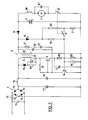
- a circuit arrangement which has an electric motor 1, which can be powered either from a battery 2 or from the AC line voltage U N.
- the AC mains voltage is connected to a rectifier 3, to which a charging capacitor 4 is connected in parallel.
- a connection of the primary winding 5 of a forward converter 6, which has a ferrite core 7, is connected to this charging capacitor 4.
- the other connection of the above-mentioned primary winding 5 is connected to the collector of a transistor 8, the emitter of which is connected to a parallel connection of capacitor 9 and resistor 10 and to a switch 11.
- the base of transistor 8 is connected via a resistor 12 to the second connection of primary winding 5, to a capacitor 13 and to the collector of a further transistor 14.
- the emitter of the transistor 14 While the emitter of the transistor 14 is grounded, its base is connected to the switch 11 and, via a resistor 15, to the cathode of a light-emitting diode 10 which is connected with its anode to a resistor 17 which is connected to the capacitor 13 .
- the anode of the diode 16 is also connected to a connection of the secondary winding 18 of the forward converter 6, the other connection of which is connected to ground.
- the anode of the diode 16 lies on the cathode of a further diode 19, the anode of which is connected to a connection of the motor 1 or the negative pole of the battery.
- a connection to ground is provided from the cathode of the diode 16 via resistors 20, 21, the connecting line between the two resistors being connected to the switch 11.
- Another switch 22, with which the motor 1 can be grounded, is also provided. The mode of operation of the circuit arrangement shown in FIG. 1 is described below, reference also being made to FIGS. 2a, 2b, 3.
- the AC line voltage U N is rectified by the rectifier 3, which can be a Graetz bridge, and smoothed by the charging capacitor 4. A voltage is then obtained at the charging capacitor 4 which corresponds to V - 2 times the effective AC voltage. If one assumes a working situation in which the circuit arrangement is at rest and the two transistors 8 and 14 block and if a DC voltage is applied to the series circuit comprising primary winding 5, transistor 8 and resistor 10, a current can flow to the base of transistor 8 via resistor 12. A few micro-amperes of base current are already sufficient to cause a switching tendency in transistor 8. This causes a small current through the primary winding 5 of the forward converter 6, which causes a change in the magnetic flux of the forward converter 6.
- a positive electrical voltage is then induced, which is applied to the base of the transistor 8 via the resistor 17 and the capacitor 13. Based on this voltage, a base current is generated, which is essentially limited by the resistor 17.
- This type of positive feedback results in an avalanche-like switch-on effect in transistor 8, so that it is practically comparable to a mechanical switch.
- the transistor 8 is switched on, the current in the primary winding 5 of the forward converter 6 increases until a voltage proportional to the current, for example of approximately 100 millivolts, is present at the resistor 10. This voltage produces a base current in transistor 14, as a result of which transistor 14 switches on and pulls the base of transistor 8 to ground or zero potential.
- the magnetic energy present in the ferrite core 6 flows out of the secondary winding 18 as current.
- the diode 19 becomes conductive and the battery 2, which consists for example of nickel-cadmium batteries, receives a line ar falling charging current.
- a negative, falling current through the resistor 17 and the capacitor 13 keeps the transistor 8 blocked until the magnetic energy stored in the core 7 has drained off. Only then can a starting current flow again via the resistor 12 into the base of the transistor 8, which triggers the switching process already described.
- a flyback converter can be implemented, the flyback phase of which depends on the voltage of the cells of the battery 2, this voltage being almost constant when viewed from the converter side.
- the core 7 always has the same energy content when switched off.
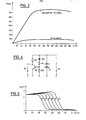
- the increase in the current I 1 in the primary winding 5 is proportional to the amount of the applied voltage U N or U 1 . Since the Ab circuit of the transistor 8 as a function of its emitter current - and thus in good approximation of current I 1 through the primary winding 5 - takes place, the circuit is forced to a change in the supply voltage U 1 . The switch-on time t 1 of the transistor 8 is therefore halved when the voltage U 1 is doubled. This results in an increase in the switching frequency and thus an increase in the effective charging current I Z of the battery 2.
- Fi g. 2a represents the case in which U 1 has a first amount U 10
- FIG. 2 b shows the case in which U 1 has twice the amount as in FIG. 2a, namely 2 U 10th
- the switch-on time t 1 is halved.
- the voltage at point A transformed by the flow converter 6 is proportional to the input voltage U 1 .
- the current flowing through the primary winding 5, the transistor 8 and the resistor 10 is superimposed on the resistor 10 by a current which is directly proportional to the supply voltage U 1 .
- the switch-off time of the transistor 8 is delayed by the transistor 14 as a function of the supply voltage U 1 .
- Point A has a potential at the resistor 10 during the time of the current and voltage rise, that of the supply voltage U 1 is proportional.
- the connection of point A via diode 16 and resistor 15 to resistor 10 enables particularly low-loss detection of supply voltage U 1 .
- a current component proportional to the supply voltage and a current component proportional to the respective emitter current of transistor 8 flow in resistor 10. The latter current component triggers the switch-off process.
- the addition of the two currents in the resistor 10 allows, with appropriate dimensioning of the resistance ratios of the resistors 15 and 10, to set a charging current I Z on the battery 2 which is independent of the supply voltage U 1 over a wide range.
- the amount of this current I Z can be z. B. by closing the switch 11, whereby the resistors 20, 21 are coupled, increase.
- the light emitting diode 16 separates the resistors 15 and 20 from point A during the blocking operation.
- This diode 16 and the addition network consisting of the resistors 20, 21, 15, 10 are live only during the switch-on phase of the transistor 8. Since the duty cycle is approximately inversely proportional to the amount of the supply voltage U 1 , the brightness of the light-emitting diode 16 is regulated automatically.
- the embodiment described here can be used to operate a DC motor for an electric shaver or the like. If the two switches 11, 22 are open, the circuit operates in the permanent charge mode. The motor 1 is at a standstill and a continuous charging current flows into the battery 2. The LED 16 also lights up. If the two switches 11, 22 are closed, the current output by the converter 6 is increased approximately tenfold, the motor 1 runs without discharging the battery 2, which now only acts as a voltage stabilizer. In addition, the LED 16 lights up.
- the control characteristic of a circuit arrangement implemented in practice is shown in FIG.
- FIG. 4 The principle of this circuit is shown in FIG. 4, a zener diode 40, a resistor 41 and a resistor 42 being connected in parallel with the nickel-cadmium cells 2.
- the base of a transistor 44 is connected to the connecting line between the two resistors 41 and 42, the emitter of which is connected to ground and the collector of which is connected to the cathode of the Zener diode 40.
- the transistor 44 begins to turn on.
- the voltage U A at the collector of transistor 44 then drops.
- FIG. 5 shows the profile of the collector voltage U A as a function of the cell voltage U Z at different temperatures.
- the temperature coefficient of the switching voltage is 5mV / ° C and is thus adapted to the temperature response of two nickel-cadmium cells 2 connected in series.
- the housing of the Zener diode 40 is thermally connected to the two nickel-cadmium cells 2.
- FIG. 7 shows a variant of Fig.l. Those elements which correspond to the elements of Fig.l are provided with the same reference numbers.
- the emitter of transistor 8 is connected to ground via a resistor 83 and two resistors 84, 85 connected in parallel, the series connection of resistors 83; 84/85 is parallel to the capacitor 9. It is also of particular importance that an arrangement is provided parallel to the primary winding 5 of the converter 6, which consists of a diode 79 and there is a resistor 80 connected in series with this diode 79, the resistor 80 being bridged by means of a zener diode 81. The zener diode 81 is connected with its anode to the anode of the diode 79.
- a capacitor 82 is connected in parallel to the series circuit comprising resistor 17 and capacitor 13.
- the circuit arrangement which is arranged parallel to the primary winding 5, essentially has the task of eliminating the peaks of the voltage flashback pulse which is formed due to the leakage inductance.
- the capacitor 82 provides a defined base voltage for the transistor 8.
Landscapes
- Engineering & Computer Science (AREA)
- Power Engineering (AREA)
- Charge And Discharge Circuits For Batteries Or The Like (AREA)
- Dc-Dc Converters (AREA)
Priority Applications (3)
| Application Number | Priority Date | Filing Date | Title |
|---|---|---|---|
| AT80106836T ATE11983T1 (de) | 1979-12-08 | 1980-11-06 | Schaltungsanordnung zum laden einer batterie. |
| US06/228,867 US4376263A (en) | 1980-11-06 | 1981-01-27 | Battery charging circuit |
| JP56024395A JPS5780238A (en) | 1980-11-06 | 1981-02-23 | Battery charging circuit |
Applications Claiming Priority (2)
| Application Number | Priority Date | Filing Date | Title |
|---|---|---|---|
| DE19792949421 DE2949421A1 (de) | 1979-12-08 | 1979-12-08 | Schaltungsanordnung zum laden einer batterie |
| DE2949421 | 1979-12-08 |
Publications (2)
| Publication Number | Publication Date |
|---|---|
| EP0030276A1 true EP0030276A1 (fr) | 1981-06-17 |
| EP0030276B1 EP0030276B1 (fr) | 1985-02-20 |
Family
ID=6087917
Family Applications (1)
| Application Number | Title | Priority Date | Filing Date |
|---|---|---|---|
| EP80106836A Expired EP0030276B1 (fr) | 1979-12-08 | 1980-11-06 | Agencement de circuit pour la charge d'une batterie |
Country Status (3)
| Country | Link |
|---|---|
| EP (1) | EP0030276B1 (fr) |
| AT (1) | ATE11983T1 (fr) |
| DE (1) | DE2949421A1 (fr) |
Cited By (8)
| Publication number | Priority date | Publication date | Assignee | Title |
|---|---|---|---|---|
| EP0056593A1 (fr) * | 1981-01-17 | 1982-07-28 | Braun Aktiengesellschaft | Dispositif de commutation pour le réglage de l'alimentation d'un appareil utilisateur |
| EP0057910A2 (fr) * | 1981-02-05 | 1982-08-18 | Braun Aktiengesellschaft | Circuit pour l'alimentation régulée d'un utilisateur |
| EP0095072A1 (fr) * | 1982-05-17 | 1983-11-30 | Braun Aktiengesellschaft | Dispositif d'alimentation à commutation électronique |
| EP0123085A2 (fr) * | 1983-03-24 | 1984-10-31 | Braun Aktiengesellschaft | Bloc d'alimentation à commutation électronique avec bobine de transformateur |
| EP0130411A2 (fr) * | 1983-07-01 | 1985-01-09 | Braun Aktiengesellschaft | Dispositif d'alimentation à découpage électronique |
| AT387875B (de) * | 1983-03-31 | 1989-03-28 | Schrack Elektronik Ag | Schaltungsanordnung zum betreiben einer last |
| WO1989007854A1 (fr) * | 1988-02-09 | 1989-08-24 | Braun Aktiengesellschaft | Procede et circuits de determination de la duree de chargement d'accumulateurs |
| EP0383381A1 (fr) * | 1989-02-14 | 1990-08-22 | Koninklijke Philips Electronics N.V. | Circuit d'alimentation |
Families Citing this family (4)
| Publication number | Priority date | Publication date | Assignee | Title |
|---|---|---|---|---|
| DE3111432A1 (de) * | 1981-03-24 | 1982-10-07 | Braun Ag, 6000 Frankfurt | Schaltungsanordnung zur geregelten speisung eines verbrauchers |
| DE3103863C2 (de) * | 1981-02-05 | 1983-03-24 | Braun Ag, 6000 Frankfurt | Schaltungsanordnung zur Speisung eines Gleichstromverbrauchers mit konstantem Strom aus Eingangsgleichspannungsquellen unterschiedlicher Spannung |
| DE3232237C2 (de) * | 1981-11-09 | 1990-10-25 | Braun Ag, 6000 Frankfurt | Elektronisches Schaltnetzteil |
| DE3230390A1 (de) * | 1982-08-14 | 1984-02-16 | odam, S.A., 67160 Wissembourg | Netzgeraet fuer einen defibrillator und defibrillator |
Citations (1)
| Publication number | Priority date | Publication date | Assignee | Title |
|---|---|---|---|---|
| DE2457664A1 (de) * | 1974-12-06 | 1976-06-10 | Bosch Gmbh Robert | Elektrische schaltungsanordnung zur erzeugung einer stabilen ausgangsspannung |
Family Cites Families (2)
| Publication number | Priority date | Publication date | Assignee | Title |
|---|---|---|---|---|
| US3435320A (en) * | 1967-02-10 | 1969-03-25 | Robert H Lee | Dc to dc converter |
| DE2948054B2 (de) * | 1979-11-29 | 1982-02-04 | Klaus Dipl.-Ing. 6239 Eppstein Becker | Schaltungsanordnung zur geregelten Speisung eines Verbrauchers |
-
1979
- 1979-12-08 DE DE19792949421 patent/DE2949421A1/de not_active Ceased
-
1980
- 1980-11-06 AT AT80106836T patent/ATE11983T1/de not_active IP Right Cessation
- 1980-11-06 EP EP80106836A patent/EP0030276B1/fr not_active Expired
Patent Citations (1)
| Publication number | Priority date | Publication date | Assignee | Title |
|---|---|---|---|---|
| DE2457664A1 (de) * | 1974-12-06 | 1976-06-10 | Bosch Gmbh Robert | Elektrische schaltungsanordnung zur erzeugung einer stabilen ausgangsspannung |
Non-Patent Citations (2)
| Title |
|---|
| ELECTRICAL DESIGN NEWS, Band 15, Nr. 2, 15. Januar 1970, Denver, US, D.A. ZINDER: "Fast-charging systems for Ni-CD batteries", Seiten 65-67 * Das ganze Dokument * * |
| ELECTRONICS, Band 51, Nr. 26, 21. Dezember 1978, New York, US, R.J. BOSCHERT: "Flyback converters solid-state solution to low-cost switching power supplies", Seiten 100-104 * Seite 102, linke Spalte, Zeile 11 bis Seite 104, linke Spalte, Zeile 23; Figuren 3-5 * * |
Cited By (12)
| Publication number | Priority date | Publication date | Assignee | Title |
|---|---|---|---|---|
| EP0056593A1 (fr) * | 1981-01-17 | 1982-07-28 | Braun Aktiengesellschaft | Dispositif de commutation pour le réglage de l'alimentation d'un appareil utilisateur |
| EP0057910A2 (fr) * | 1981-02-05 | 1982-08-18 | Braun Aktiengesellschaft | Circuit pour l'alimentation régulée d'un utilisateur |
| EP0057910A3 (en) * | 1981-02-05 | 1983-05-04 | Braun Aktiengesellschaft | Circuit for the regulated supply to a user |
| EP0095072A1 (fr) * | 1982-05-17 | 1983-11-30 | Braun Aktiengesellschaft | Dispositif d'alimentation à commutation électronique |
| EP0162341A1 (fr) * | 1982-05-17 | 1985-11-27 | Braun Aktiengesellschaft | Dispositif d'alimentation à commutation électronique |
| EP0123085A2 (fr) * | 1983-03-24 | 1984-10-31 | Braun Aktiengesellschaft | Bloc d'alimentation à commutation électronique avec bobine de transformateur |
| EP0123085B1 (fr) * | 1983-03-24 | 1988-07-13 | Braun Aktiengesellschaft | Bloc d'alimentation à commutation électronique avec bobine de transformateur |
| AT387875B (de) * | 1983-03-31 | 1989-03-28 | Schrack Elektronik Ag | Schaltungsanordnung zum betreiben einer last |
| EP0130411A2 (fr) * | 1983-07-01 | 1985-01-09 | Braun Aktiengesellschaft | Dispositif d'alimentation à découpage électronique |
| EP0130411A3 (en) * | 1983-07-01 | 1986-01-29 | Braun Aktiengesellschaft | Electronic switching power supply |
| WO1989007854A1 (fr) * | 1988-02-09 | 1989-08-24 | Braun Aktiengesellschaft | Procede et circuits de determination de la duree de chargement d'accumulateurs |
| EP0383381A1 (fr) * | 1989-02-14 | 1990-08-22 | Koninklijke Philips Electronics N.V. | Circuit d'alimentation |
Also Published As
| Publication number | Publication date |
|---|---|
| DE2949421A1 (de) | 1981-07-02 |
| EP0030276B1 (fr) | 1985-02-20 |
| ATE11983T1 (de) | 1985-03-15 |
Similar Documents
| Publication | Publication Date | Title |
|---|---|---|
| EP0162341B1 (fr) | Dispositif d'alimentation à commutation électronique | |
| EP0030026B1 (fr) | Agencement de circuit pour l'alimentation stabilisée d'un utilisateur | |
| DE2524790C3 (de) | Schaltungsanordnung für ein Batterieladegerät | |
| EP0186865B1 (fr) | Dispositif d'interruption de décharges en arc dans une enceinte à décharge dans un gaz | |
| EP0030276A1 (fr) | Agencement de circuit pour la charge d'une batterie | |
| EP0226128B1 (fr) | Alimentation à découpage électronique | |
| DE3515998A1 (de) | Elektrische einrichtung, die mit einer batterieladeanordnung verbunden ist | |
| EP0057910B1 (fr) | Circuit pour l'alimentation régulée d'un utilisateur | |
| DE4208911B4 (de) | Spannungsversorgung | |
| DE3630421C2 (fr) | ||
| DE3101375A1 (de) | Schaltungsanordnung zur geregelten speisung eines verbrauchers | |
| DE2948054A1 (de) | Schaltungsanordnung zur geregelten speisung eines verbrauchers | |
| EP0593518B1 (fr) | Unite electronique d'alimentation en energie fournie par le reseau electrique | |
| DE2014377A1 (de) | Transistor-Wandlerschaltung | |
| DE2402182B2 (de) | Ladegerät für Akkumulatoren | |
| DE1935201C3 (de) | Schaltungsanordnung zum Schnelladen einer elektrischen Batterie | |
| WO1990003059A1 (fr) | Chargeur d'accumulateurs | |
| DE3103863C2 (de) | Schaltungsanordnung zur Speisung eines Gleichstromverbrauchers mit konstantem Strom aus Eingangsgleichspannungsquellen unterschiedlicher Spannung | |
| EP0320605B1 (fr) | Alimentation électronique à découpage avec un convertisseur à inductance | |
| DE2457999C3 (de) | Von einem Wechselspannungsgenerator gespeister Schwingmotor | |
| DE4212041A1 (de) | Elektronisches Schaltnetzteil | |
| DE1803840C3 (de) | Spannungsregler für einen permanentmagnetisch erregten Wechselstromgenerator | |
| DE3803906A1 (de) | Verfahren und schaltungsanordnung zur bestimmung der ladezeit eines akkumulators | |
| CH665506A5 (de) | Schaltungsanordnung zum betreiben einer last. | |
| DE2513287A1 (de) | Gleichspannungswandler |
Legal Events
| Date | Code | Title | Description |
|---|---|---|---|
| PUAI | Public reference made under article 153(3) epc to a published international application that has entered the european phase |
Free format text: ORIGINAL CODE: 0009012 |
|
| AK | Designated contracting states |
Kind code of ref document: A1 Designated state(s): AT CH FR GB IT NL Designated state(s): AT CH FR GB IT NL |
|
| 17P | Request for examination filed |
Effective date: 19810707 |
|
| ITF | It: translation for a ep patent filed |
Owner name: DE DOMINICIS & MAYER S.R.L. |
|
| GRAA | (expected) grant |
Free format text: ORIGINAL CODE: 0009210 |
|
| AK | Designated contracting states |
Kind code of ref document: B1 Designated state(s): AT CH FR GB IT LI NL Designated state(s): AT CH FR GB IT LI NL |
|
| REF | Corresponds to: |
Ref document number: 11983 Country of ref document: AT Date of ref document: 19850315 Kind code of ref document: T |
|
| ET | Fr: translation filed | ||
| PLBI | Opposition filed |
Free format text: ORIGINAL CODE: 0009260 |
|
| PLBI | Opposition filed |
Free format text: ORIGINAL CODE: 0009260 |
|
| 26 | Opposition filed |
Opponent name: N.V. PHILIPS' GLOEILAMPENFABRIEKEN Effective date: 19851120 |
|
| 26 | Opposition filed |
Opponent name: SCHRACK ELEKTRONIK-AKTIENGESELLSCHAFT Effective date: 19851119 |
|
| NLR1 | Nl: opposition has been filed with the epo |
Opponent name: SCHRACK ELEKTRONIK-AKTIENGESELLSCHAFT Opponent name: N.V. PHILIPS' GLOEILAMPENFABRIEKEN |
|
| PGFP | Annual fee paid to national office [announced via postgrant information from national office to epo] |
Ref country code: AT Payment date: 19861030 Year of fee payment: 7 |
|
| PGFP | Annual fee paid to national office [announced via postgrant information from national office to epo] |
Ref country code: NL Payment date: 19871130 Year of fee payment: 8 |
|
| RDAG | Patent revoked |
Free format text: ORIGINAL CODE: 0009271 |
|
| STAA | Information on the status of an ep patent application or granted ep patent |
Free format text: STATUS: PATENT REVOKED |
|
| 27W | Patent revoked |
Effective date: 19890502 |
|
| REG | Reference to a national code |
Ref country code: CH Ref legal event code: PL |
|
| GBPR | Gb: patent revoked under art. 102 of the ep convention designating the uk as contracting state | ||
| NLR2 | Nl: decision of opposition |