EP0215490A2 - AFC-Anordnung für Breitband-FM-Empfänger - Google Patents
AFC-Anordnung für Breitband-FM-Empfänger Download PDFInfo
- Publication number
- EP0215490A2 EP0215490A2 EP86112956A EP86112956A EP0215490A2 EP 0215490 A2 EP0215490 A2 EP 0215490A2 EP 86112956 A EP86112956 A EP 86112956A EP 86112956 A EP86112956 A EP 86112956A EP 0215490 A2 EP0215490 A2 EP 0215490A2
- Authority
- EP
- European Patent Office
- Prior art keywords
- frequency
- signal
- comparison
- center
- error range
- Prior art date
- Legal status (The legal status is an assumption and is not a legal conclusion. Google has not performed a legal analysis and makes no representation as to the accuracy of the status listed.)
- Granted
Links
Images


Classifications
-
- H—ELECTRICITY
- H03—ELECTRONIC CIRCUITRY
- H03J—TUNING RESONANT CIRCUITS; SELECTING RESONANT CIRCUITS
- H03J7/00—Automatic frequency control; Automatic scanning over a band of frequencies
- H03J7/02—Automatic frequency control
- H03J7/04—Automatic frequency control where the frequency control is accomplished by varying the electrical characteristics of a non-mechanically adjustable element or where the nature of the frequency controlling element is not significant
- H03J7/06—Automatic frequency control where the frequency control is accomplished by varying the electrical characteristics of a non-mechanically adjustable element or where the nature of the frequency controlling element is not significant using counters or frequency dividers
- H03J7/065—Automatic frequency control where the frequency control is accomplished by varying the electrical characteristics of a non-mechanically adjustable element or where the nature of the frequency controlling element is not significant using counters or frequency dividers the counter or frequency divider being used in a phase locked loop
Definitions
- the present invention relates to an A.F.C. (automatic frequency control) system for an FM radio receiver, and in particular to an A.F.C. system for a receiver to be utilized for reception of broad-band FM signals transmitted from an earth satellite.
- A.F.C. automatic frequency control
- the accuracy with which the frequency of the local oscillator is maintained will be identical to that of the reference frequency signal of the frequency synthesizer circuit.
- a quartz crystal oscillator is utilized to produce the reference frequency signal, so that if the frequency accuracy of the recived signal is sufficiently high, a satisfactory degree of frequency accuracy for the I.F. (intermediate frequency) signal will be attained without the need to incorporate an A.F.C. system in the receiver.
- the received microwave band signal is first converted into a first I.F. signal by a down-converter (positioned close to the antenna, i.e.
- the first I.F. signal is then converted to a second I.F. signal within the receiver.
- Tuning i.e. selection of a desired reception channel, is performed by the process of frequency conversion into the second I.F. signal, through variation of the frequency of the local oscillator signal which is employed in this conversion.
- the term "local oscillator” will be restricted to signifying the local oscillator whose signal is utilized in producing the second I.F. signal, while the second I.F. signal will be simply referred to as the I.F. signal.
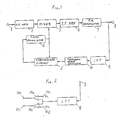
- Fig. 1 is a block diagram of this prior art example, in which reference numeral 1 denotes a received signal input terminal, numeral 2 denotes a H.F. amplifier, numeral 3 denotes a frequency mixer, numeral 4 denotes a voltage-control type of local oscillator, numeral 5 denotes a PLL (phase lock loop) type of frequency synthesizer circuit, numeral 6 denotes an I.F.
- reference numeral 1 denotes a received signal input terminal
- numeral 2 denotes a H.F. amplifier
- numeral 3 denotes a frequency mixer
- numeral 4 denotes a voltage-control type of local oscillator
- numeral 5 denotes a PLL (phase lock loop) type of frequency synthesizer circuit
- numeral 6 denotes an I.F.
- Fig. 2 shows an example of a circuit for the frequency error detection circuit 10, in which the demodulated output signal from the FM demodulator 7 is smoothed by transfer through a LPF 9, to thereby derive the DC component of the demodulated signal. This DC component is compared with fixed reference voltage levels V r 1 and V r 2 in a pair of voltage comparators 10a and 10b respectively.
- the DC component of the demodulated FM signal which is output from LPF 9 represents the average voltage level of the demodulated FM signal.
- This average voltage level corresponds to the average frequency of the I.F. signal which is produced by mixer 3.
- this average voltage level By comparing this average voltage level with the predetermined reference voltage levels V r 1 and V r 2 by the circuit shown in Fig. 2, it can be determined whether the center frequency of the I.F. signal has drifted from a predetermined I.F. frequency by more than a predetermined frequency range.
- the circuit detects the direction of this frequency outside the predetermined range, i.e. the output signals from terminals 10e, 10f respectively indicate whether the center frequency of the I.F. signal frequency is lower than or higher than the specified I.F. frequency.
- the output signals from terminals 10e and 10f are applied to the PLL frequency synthesizer circuit 5, which responds by performing fine adjustment of the frequency of oscillation of the local oscillator 4 such as to counteract the frequency drift, i.e. to maintain the amount of frequency drift outside the predetermined range to a sufficiently small amount.
- the frequency reference for A.F.C. system operation is constituted by the demodulator circuit 7 itself.
- the FM demodulator does not display very good temperature stability, with respect to the relationship between input frequency and output voltage, since the most important design requirement for such a demodulator is that it must be capable of handling high-frequency wide-band FM signals. For this reason, it is difficult to realize an A.F.C. system of the form shown in Fig. 1 which will maintain a high degree of I.F. signal frequency accuracy.
- the FM signal must maintain a high degree of linearity in the demodulation process, as is true in the case of a video signal, then it is extremely important to ensure that amplitude and phase errors do not arise. If I.F. frequency drift occurs, then such errors will be produced as a result of passing the FM I.F. signal through the I.F. band-pass filter.
- A.F.C. system having the objective of overcoming the problems described above.
- A.F.C. system a highly accurate reference frequency signal is utilized as a frequency reference.
- the FM I.F. signal is applied to the inputs of two frequency dividers having respectively different frequency division ratios. These frequency division ratios and the frequency of the reference frequency signal are selected such that, when the I.F. signal center frequency coincides with an upper limit frequency (which is higher than a predetermined I.F. frequency by a specific amount), the output of one of the frequency dividers will coincided in frequency with the reference signal, and such that when the I.F.
- the output of the other frequency divider will coincide in frequency with the reference signal.
- Two frequency comparators are also utilized, with the reference frequency signal being applied to one input of each of these frequency comparators and the outputs from the frequency dividers being respectively applied to the other inputs of the frequency comparators.
- the resultant outputs signals from the frequency comparators are passed through respective integrator circuits or low-pass filters, to thereby produce two frequency comparison signals, whose levels indicate the frequency relationship between the reference frequency signal and the I.F. signal.
- These signals are applied to a frequency synthesizer circuit which produces a control voltage to control the local oscillator frequency, to thereby implement fine adjustment of that control voltage and hence fine control of the local oscillator frequency and hence the I.F. frequency, in accordance with the frequency relationship between the reference frequency signal and the I.F. signal.
- the output frequency from the frequency divider having the division ratio N L will become lower than f L /N L , and so (from equation (2) above) will become lower than the reference signal frequency F S .
- the output from the frequency comparator which receives the latter frequency divider output and the reference frequency signal will indicate that the center frequency of the I.F. signal has become lower than the lower detection limit f L .
- the output signals from the frequency comparators are then passed through simple integrator circuits (or low-pass filters) to derive the DC component of each signal, to thereby obtain two frequency comparison signals.
- One of these frequency comparison signal will change between a high and a low logic level when the amount of error of the center frequency of the I.F. signal reaches the upper detection limit f H , while the other frequency comparison signal will similarly change in logic level when the I.F. signal reaches the lower detection limit f L .
- the combination of these two frequency comparison signal can be utilized to judge which of three possible conditions is currently true of the center frequency f C of the I.F. signal, i.e.
- the frequency comparison signal can be utilized to judge whether fine adjustment of the local oscillator frequency should be performed (i.e. by fine adjustment of the control voltage applied to the local oscillator in the case of a receiver employing a synthesizer circuit to produce such a control voltage), and also the direction in which this fine adjustment of the local oscillator frequency is to be executed.
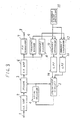
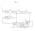
- A.F.C. system is shown in the block diagram of Fig. 3.
- a received signal i.e. from a down-converter
- H.F. amplifier to a mixer
- I.F. signal which is applied to an FM demodulator 7.
- a synthesizer circuit 5 such as a PLL type of frequency synthesizer, produces a frequency control voltage which is applied to a local oscillator 4 to control the local oscillator frequency which is applied to mixer 3.
- the I.F. signal is supplied to each of two frequency dividers 9 and 10, which have respective frequency division ratios N H and N L .
- the resultant output signals from frequency dividers 9 and 10 are applied to inputs of two frequency comparators 12 and 13 respectively, while a reference frequency produced from a reference signal oscillator 11 at a frequency F S is applied to each of the other inputs of the frequency comparators 12 and 13.
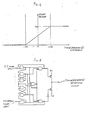
- Each of the frequency comparators 12 and 13 can be of digital type, for example having the configuration shown in Fig. 5.
- Such a frequency comparator displays a relationship between phase (frequency) and the DC component of the output therefrom having the form shown in Fig. 4.
- the outputs from frequency comparators 12 and 13 are transferred through respective low-pass filters (LPFs) 14 and 15, to remove AC components of the comparator output signals and thereby produce respective frequency comparison signals.
- LPFs low-pass filters
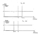
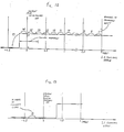
- Figs. 6A and 6B are graphs showing the variation of of the frequency comparison signals produced from LPFs 14 and 15 respectively, in which I.F. signal center frequency are plotted along the horizontal axis and the level of the frequency comparison signal along the vertical axis. Designating the specified center frequency of the I.F. signal as f O , the reference frequency frequency and the frequency division ratios N H , N L must satisfy the following relationship F S x N L ⁇ f O ⁇ F S x N H
- the center frequency of the I.F. signal will be higher than the specified frequency by an amount which exceeds a predetermined limit frequency (F S x N H ).
- F S x N H a predetermined limit frequency
- the second frequency comparison signal i.e the output from LPF 15
- the synthesizer circuit 5 must therefore apply correction to the local oscillator frequency in a direction to correct this frequency error.
- each of the quantities (F S x N H - f O ), and (f O - F S x N L ) should be selected to be within 300 kHz.
- the specified center frequency of the I.F. signal f O is 510 MHz
- the reference frequency frequency F S is 10 kHz
- one of the frequency division ratios N H is 51030 and the other frequency division ratio N L is 50970
- the I.F. signal is frequency divided by two frequency dividers having mutually different frequency division ratios, and the frequency-divided output signals are compared in frequency with a reference frequency, whereby a frequency error which causes the center frequency of the I.F. signal to depart from a predetermined frequency error range (centered on the specified if frequency) can be accurately detected.
- the frequency stability of this system is determined by the reference frequency, so that if a highly stable and accurate oscillator circuit such as a quartz crystal controlled oscillator is utilized to produce the reference frequency, an A.F.C. system can be realized which has a high degree of frequency control accuracy.
- an automatic frequency control system has the function of performing correction of a frequency error of a center frequency of a frequency-modulated intermediate frequency signal with respect to a predetermined intermediate frequency value such as to hold the magnitude of said frequency error within a predetermined frequency error range.
- Such an automatic frequency control system is for use in frequency modulation receiver system which includes local oscillator circuit means for producing a local oscillator signal and a mixer coupled to receive the local oscillator signal for producing the frequency-modulated intermediate frequency signal, the automatic frequency control system comprising: control means: frequency comparison means controlled by the control means to selectively operate in a first status for comparing the center frequency of the intermediate frequency signal with an upper limit frequency of the frequency error range and in a second status for comparing the center frequency of the intermediate frequency signal with a lower limit of the frequency error range, and for producing a frequency comparison signal indicative of results of the frequency comparisons; first and second latch memory means controlled by the control means to store the frequency comparison signal as data indicative of the relationship between the center frequency of the intermediate frequency signal and the upper and lower limit frequencies, and; frequency adjustment means controlled by the control means for adjusting the local oscillator frequency; the control means acting, following the frequency comparison operation, to judge whether the data stored in the first and second latch memory means indicates that the center frequency of the intermediate frequency signal is within the frequency error range, and
- the control means acts, when the center frequency of the intermediate frequency signal is judged to be higher than the upper frequency limit as indicated by the data stored in the first and second latch memory means, to repetitively execute a series of operations comprising: comparison of the center frequency of the intermediate frequency signal with the upper frequency limit; storage of the frequency comparison signal level in the first latch memory means, and; controlling the frequency adjustment means such as to decrease the local oscillator frequency by a fixed amount, and in which the control means acts, when the center frequency of the intermediate frequency signal is judged to be lower than the lower frequency limit, as indicated by the data stored in the first and second latch memory means, to repetitively execute a series of operations comprising: comparison of the center frequency of the intermediate frequency signal with the lower frequency limit; storage of the frequency comparison signal level in the second latch memory means, and; controlling the frequency adjustment means such as to increase the local oscillator frequency by a fixed amount.
- An A.F.C. system employs a highly stable reference frequency as a frequency reference, with the reference frequency and an I.F. signal being applied to respective variable frequency dividers to thereby produce a frequency-divided I.F. signal and a frequency-divided reference signal which are applied to the inputs of a frequency comparator.
- the output signal from the frequency comparator is passed through a low-pass filter to thereby derive the frequency comparison signal, which is applied to respective inputs of two latch memory circuits.
- the frequency division ratios of the variable frequency dividers are respectively controlled by a controller to selectively establish two different combinations of these frequency division ratios, while the controller also controls latch operations by the latch memory circuits.
- the values of the reference frequency and the frequency division ratios are selected such that, with one of these combinations of frequency division ratios established by the controller, the center frequency of the intermediate frequency signal is, in effect, compared with the upper frequency limit referred to above, while with the other combination of frequency division ratios established, the center frequency of the intermediate frequency signal is, in effect, compared with the lower frequency limit referred to above.
- a received FM signal (e.g. supplied from a down-converter) is applied from an input terminal 1 through an H.F. amplifier 2 to a mixer 3, to produce a FM I.F. signal which is passed through an I.F. amplifier 6 to be demodulated by a FM demodulator 7.
- a demodulated FM signal thereby appears on an output terminal 8.
- the frequency of oscillation of a voltage-controlled local oscillator 4 is determined by a control voltage which is produced by a frequency control voltage synthesizer circuit 5.
- frequency control voltage synthesizer circuit 5 and local oscillator 4 will be assumed in the following to constitute a PLL (phase lock loop) circuit, however the invention is also applicable to a receiver system employing a voltage synthesizer circuit for control of the local oscillator frequency which employs a digital/analog converter to produce a frequency control voltage, for example.
- PLL phase lock loop
- a reference frequency of high frequency accuracy is generated by a reference frequency oscillator 11, which employs a quartz crystal vibrator element 21.
- the oscillation frequency of reference signal oscillator 11 will be designated as F S .
- the reference frequency and I.F. signal are supplied to variable frequency dividers 22 and 23 (i.e. frequency dividers whose respective division ratios can be controllably set to at least two different values) respectively, and whose output signals are applied to a frequency comparator 24.
- the circuit section 25 shown surrounded by a broken-line outline in Fig. 7 is a PLL (phase lock loop) LSI section in this embodiment i.e. a circuit portion contained within a generally used type of frequency synthesizer circuit formed in an integrated circuit.
- the frequency division ratios of the variable frequency dividers 22 and 23 are controlled by a signal applied from a controller 27, which is implemented externally to the LSI section 25.
- the variable frequency divider 22 can be set to either of two frequency division ratios designated as N IH and N IL , while the variable frequency divider 23 can be set to two frequency division ratios N SH and N SL .
- the frequency comparator 24 is preferably of digital configuration, e.g. as shown in Fig.
- the logic level of the frequency comparison signal from LPF 26 is memorized in each of a pair of latch memory circuits 28 and 29, at timings determined by signals applied to the latch memory circuits 28 and 29 from the controller 27.
- the relationships between the output signals from latch memory circuits 28 and 29, i.e. the frequency comparison signal levels memorized therein, and the I.F. signal frequency, are shown in Figs. 8A and 8B.
- controller 27 controls the operation of the variable frequency dividers 22 and 23 such as successively and alternately switch this operation between a first operating status in which the variable frequency dividers of the variable frequency dividers 22 and 23 are N IH and N SH respectively, and a second status in which these variable frequency dividers are N IL and N SL respectively. After the first status has been established, so that the center frequency of the I.F.
- the controller 27 waits for a sufficient length of time (detection delay time, as described hereinafter) for the output signal level from LPF 26, i.e. the frequency comparison signal, to attain a level which correctly represents the result of this frequency comparison operation. If the center frequency of the I.F. signal is lower than the upper frequency limit f H , then when comparison is performed with the frequency division ratios set to N IH and N SH the frequency comparison signal will be at the L level, so that this L level state is stored as data in latch memory circuit 28, while if the center frequency of the I.F. signal is higher than f H then the frequency comparison signal will be at the H level, and this state will be stored in latch memory circuit 28.
- the controller 27 waits for the detection delay time to elapse, and then stores the output signal level from LPF 26, i.e. the frequency comparison signal level, in latch memory circuit 29. If the center frequency of the I.F. signal is lower than the lower frequency limit f L , then the frequency comparison signal will be at the L level in this case , so that an L level state is stored as data in latch memory circuit 29 while if the center frequency of the I.F. signal is higher than f L , the frequency comparison signal will be at the H level, and this state will be stored in latch memory circuit 29.
- FIGs. 8A and 8B the combination of data stored in latch memories 28 and 29 (and hence the output signal levels produced by latch memories 28 and 29 respectively) following such a data storage operation will indicate the current relationship between the center frequency of the I.F. signal and the predetermined frequency error range. That is to say, if the output signal from latch memory circuit 29 is at the L level, then this indicates that the center frequency of the I.F. signal is below the lower frequency limit f L , i.e. the data contents of latch memory circuits 28 and 29 indicate that the center frequency of the I.F. signal must be adjusted upwards, to bring that frequency back within the frequency error range.
- the output signal from latch memory circuits 28 is at the H level, then this indicates that the center frequency of the I.F. signal is higher than the upper limit frequency f H , so that the center frequency must be adjusted downwards. If on the other hand the output signal from the latch memory circuit 28 is at the L level while the output signal from latch memory circuit 29 is at the H level, then this indicates that the center frequency of the I.F. signal is within the predetermined frequency error range, so that no adjustment of the center frequency is necessary.
- the synthesizer circuit 5 makes a judgement as to whether the combination of data stored in latch memory circuit 28 and latch memory circuit 29 indicates that the center frequency of the I.F. signal is within the predetermined frequency error range, or whether the data indicates that correction of the center frequency is required. If correction is required, then the synthesizer circuit 5 judges from the stored data in latch memory circuits 28 and 29 the direction required for this correction.
- the synthesizer circuit 5 applies a fixed change in voltage to the frequency control voltage supplied to local oscillator 4, with the direction of this voltage change and hence the direction of the resultant frequency change of the local oscillator frequency being determined by the direction of correction required, and with the amplitude of the change in frequency control voltage (and hence the amplitude of the resultant change in local oscillator frequency) being a fixed quantity.
- the synthesizer circuit 5 acts to lower the local oscillator frequency by a fixed amount (e.g. 200 kHz).
- the frequency division ratios of the variable frequency dividers 22 and 23 are held unchanged, and after the requisite detection delay time, the frequency comparison signal state is stored in latch memory circuit 28.
- controller 27 and the synthesizer circuit 5 have been described as operating mutually separately. However in an actual A.F.C. system most of the functions performed by controller 27 and synthesizer circuit 5, other than the production of a frequency control voltage, can be executed by a single control means, i.e. by a single microprocessor which has been suitably programed.
- the degree of frequency control accuracy provided by the A.F.C. circuit should be within approximately ⁇ 300 kHz, i.e. the frequency error range should ⁇ 300 kHz with respect to the specified center frequency of the I.F. signal.
- each of the quantities (F S ⁇ N IH /N SH - f O ), and (f O - F S ⁇ N IL /N SL ) should be selected to be within 300 kHz.
- each of the frequency division ratios N IH and N IL should be made equal to approximately 50,000.
- the specified I.F. frequency is 510 MHz
- the frequency of the reference frequency is 4 MHz
- the I.F. signal is applied directly to a variable frequency divider 22 which is contained within a PLL-LSI section 25.
- preliminary frequency division of the I.F. signal can be performed using a pre-scaler before the I.F. signal is supplied to PLL-LSI section 25.
- the overall frequency division ratio for the fis will be the product of the frequency division ratio of the pre-scaler and the variable frequency divider which is contained within the PLL-LSI section 25.
- the frequency division ratios of variable frequency divider 23 and N SH N SL .
- the pre-scaler is used for the reference frequency, and this has a frequency division ratio of N p
- the actual frequency division ratios applied to the reference frequency will be N P ⁇ N SH and N P ⁇ N SL .
- N SH and N SL can be arbitrarily selected.
- the first embodiment of the present invention described above with reference to Fig. 7 provides the advantage of highly accurate frequency control, as does the example of Fig. 3.
- the embodiment of the present invention shown in Fig. 7 has the further advantage of a more simple circuit configuration, since it is only necessary to use a single frequency comparator and a single low-pass filter.
- an A.F.C. system according to the present invention can be manufactured at lower cost than an A.F.C. system such as that of Fig. 3.
- the modulation index of the I.F. signal in a receiver for reception of wide-band FM signals is fairly high. This can result in erroneous operation of the frequency comparator of an A.F.C. system according to the present invention, if the frequency comparator is of digital type having the configuration of Fig. 5 and the input/output characteristic of Fig. 4. In order to sufficiently reduce the modulation index of the frequency-divided I.F. signal therefore, it is necessary to make the frequency division ratios N IH and N IL sufficiently high, in order to ensure correct operation of the frequency comparator.
- an energy dispersal signal is superimposed on the video signal before transmission, in order to prevent certain reception failure conditions, which do not arise in the case of land-based microwave radio communication systems.
- the frequency of the energy dispersal signal is typically 30 Hz, producing a corresponding FM modulation deviation of 2 MHz p-p (approximately).
- the modulation index resulting from the energy dispersal signal is approximately 67,000.
- frequency division ratios which are each greater than approximately 50,000 for the I.F. signal variable frequency divider. Due to the use of such a high value of frequency division ratio, the frequency difference between the frequency-divided I.F.
- the signal and reference frequency at input to the frequency comparator will be only 1/50,000 of the difference between the detection limit frequencies F S ⁇ N IH /N SH and F S ⁇ N IL /N SL .
- frequency difference of 300 kHz within the I.F. band will be converted into a frequency difference of 6 Hz at input to the frequency comparator, so that the frequency comparator output will contain a 6 Hz component.
- the integrating means i.e. LPF 26 in the above embodiment
- LPF 26 the integrating means
- the detection delay time should be made approximately one second, if the frequency accuracy is to be held to 50 kHz, i.e. if correction overshoot resulting from A.F.C. operation is to be limited to 50 kHz.
- A.F.C. pull-in operation i.e. operation to bring the center frequency of the I.F. signal within the predetermined frequency error range after that center frequency has been moved substantially out of the frequency error range as a result of a tuning operation to change the reception channel.
- the maximum pull-in range of the A.F.C. system is 3 MHz
- the center frequency of the I.F. frequency is in error by 3 kHz relative to the predetermined I.F. frequency
- the frequency control accuracy is to be 50 kHz (so that a 1-second detection delay time is required) and that fine-adjustment frequency control of the local oscillator frequency is performed in discrete frequency shifts, each of 200 kHz.
- the center frequency of the I.F. signal will be moved in successive steps of 200 kHz by the control operation of controller 27 and synthesizer circuit 5, as described hereinabove, i.e. by successive steps of fine frequency adjustment of the local oscillator frequency by 200 kHz.
- This process is illustrated in Figs. 10A and 10B.
- a total of 14 of such frequency shifts will be required before the center frequency of the I.F. signal is pulled into the frequency error range, i.e. until A.F.C. lock operation is achieved.
- the block designated as frequency error detection circuit 36 consists of the combination of circuit blocks in the embodiment of Fig. 7 which receive the I.F. signal and produce as outputs the first and second latch memory circuits from latch memory circuits 28 and 29 respectively over output lines designated as 28a and 28b respectively, i.e. controller 27, variable frequency dividers 22 and 23, reference signal oscillator 11, frequency comparator 24, LPF 26 and latch memory circuits 28, 29.
- block 36 would correspond to the combination of blocks which receive the I.F. signal from I.F. amplifier 6 and produce frequency comparison signals from LPFs 14 and 15.
- Numeral 35 denotes a synthesizer circuit for determining and adjusting a frequency control voltage which is applied to a local oscillator 4, in accordance with a combination of output signals applied over latch memory output lines 29a, 29b, as in the case of the first embodiment described with reference to Fig. 7.
- Numeral 37 denotes a controller, having essentially the same functions as those of controller 27 of the first embodiment described above, but in addition having the function of determining the value of a variable detection delay time, as described hereinafter.
- Numeral 34 denotes an input terminal which is coupled to receive a tuning command signal, i.e.
- the controller 37 and synthesizer circuit 35 are each coupled to receive this tuning command signal from terminal 34.
- the controller 37 sets the detection delay time (i.e. the delay time between produced by the signal input section 35a to one of two different values, one of which is substantially lower than the other, in accordance with whether the system is operating in an A.F.C. pull-in condition or has achieved A.F.C. control. Specifically, during continuous reception of a specific channel, i.e. normal reception operation, this delay time is held at a sufficiently large value to ensure a high requisite degree of frequency control accuracy.
- this frequency control accuracy will be assumed to be 50 kHz, so that a detection delay time of one second is required during normal A.F.C. control operation.
- the center frequency of the I.F. signal of the newly selected channel will in general be substantially displaced from the specified I.F. frequency, and so must be brought towards that frequency by A.F.C. pull-in operation.
- controller 37 acts to change the detection time delay to a value which is substantially shorter than that for normal operation, e.g preferably in the range of 0.1 to 0.3 times the delay value for normal operation.
- A.F.C. pull-in is accomplished in a substantially shorter time.
- controller 37 immediately changes the detection delay time to the normal value (i.e. one second, in the example given above). Due to this immediate restoration of the normal delay time, the next frequency shift executed by the synthesizer circuit 35 will not result in a large overshoot of the center frequency of the I.F. signal beyond the frequency error range, as would otherwise occur. Thereafter, with the center frequency of the I.F. signal now brought within the predetermined frequency error range, normal A.F.C. operation to hold the I.F. frequency within that range is executed as described hereinabove with reference to the first embodiment.
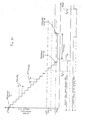
- This A.F.C. pull-in operation of the second embodiment is illustrated in Figs. 12, 13 and 14. It is assumed that, following a tuning operation to change to a new channel frequency, the center frequency of the I.F. signal is displaced from the specified I.F. frequency by 3 MHz, and that the amount of each frequency adjustment shift is limited to 200 kHz.
- the controller 37 changes the delay time produced by the signal input section 35c from the normal value (e.g. 1 second) to a shorter value which will be assumed to be 0.1 seconds. Thereafter, each of the 200 kHz successive shifts in the center frequency of the I.F. signal which are numbered from 1 to 17 in Figs. 12 to 14 will occur at intervals of 0.1 seconds.
- the center frequency of the I.F. signal will fall below the upper frequency limit f H of the frequency error range, which in this example is +300 kHz with respect to the predetermined center frequency.
- the output from latch memory circuit 28 will only change from the H to the L level (indicating that the center frequency has come below the upper frequency limit) at a subsequent time indicated as t B in Fig. 14, i.e. after the 17'th 200 kHz frequency shift has been initiated, in this example.
- the detection delay time is immediately changed to 1 second.
- the subsequent one-second detection delay time will allow the frequency control signal (and hence the output from latch memory 29) to fall from the H to the L level before the memory contents are next judged by controller 37.
- controller 37 recognizes from the L level condition of the output from latch memory 29 that the center frequency of the I.F. signal has fallen below the lower limit frequency f L .
- the next 200 kHz frequency shift i.e. the 18'th serves to increase the center frequency, and so bring that frequency within the frequency error range.
- A.G.C. pull-in operation has been completed, as indicated by the output signal from latch memory 28 being at the L level and that from latch memory 29 being at the H level.
- the delay time during A.F.C. pull-in operation is set to 0.3 seconds rather than 0.1 seconds in the above example, then the total time required for completion of pull-in would be appoximately 5 seconds.
- the inventor has found that the shortened detection delay time during A.F.C. pull-in operation should preferably be within the range of 0.1 to 0.3 times the value of detection delay time which is established during normal A.F.C. operation.
- the controller directly utilizes the data contents of latch memories 28 and 29, with the combination of levels of these data contents representing whether the center frequency of the I.F. signal is within or outside the frequency error range.
- a circuit for converting the data held in latch memory 28 and 29, i.e. the output signals form latch memory 28 and 29 representing that data into a correction indication signal whose level indicates whether correction of the center frequency of the I.F. signal is required, and correction direction signals which indicate the required direction for such correction.
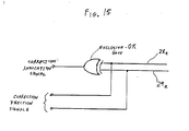
- An example of a circuit to perform this function is shown in Fig. 15.
- Output signals from latch memories 28 and 29 are supplied over lines 28a, 29a respectively to the inputs of an exclusive-OR gate, which thereby produces an output signal at the L level if no correction of the I.F. center frequency is required, and at the H level if correction is required.
- the output signals from latch memory 28 and latch memory 29 can be directly employed as correction direction signals, as will be apparent from the description given hereinabove with reference to Figs. 8a and 8B.
- controller 27 and of at least a part of synthesizer circuit 5, in the first embodiment of the invention shown in Fig. 7, can be implemented by a digital microprocessor.
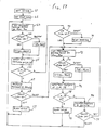
- Fig. 16 is a flow diagram to illustrate the operation of such a micoprocessor.
- the microprocessor system enters the operation flow shown in Fig. 17, at step 41.
- the system sets the frequency division ratios of the variable frequency dividers 22 and 23 to be N IH and N SH respectively.
- step 42 waiting is performed for a detection delay time of 1 second. This is the time required for a change in level of the output signal (DC component) from frequency comparator 24 to result in a change in logic level of the frequency comparator signal from LPF 26.
- step 43 the stored contents of latch memory (indicated as L.M.) 28 are read into the system.
- a decision is then made, in step 44, as to whether the latch memory contents are at the H or the L level. If they are at the H level then this indicates that the center frequency of the I.F. signal is higher than the upper limit frequency f H , in which case step 45 is executed.
- step 46 the system sets the frequency division ratios of the variable frequency dividers 22 and 23 to N IL AND N SL .
- step 47 the contents of latch memory 29 are read in.
- step 49 the level of the latch memory 29 data
- step 46 the system commands the synthesizer circuit 5 to increase the local oscillator frequency by 200 kHz. Operation then returns to step 46.
- the loop of steps from 46 to 50 is then cyclically repeated, until it is determined in step 49 that the contents of latch memory 29 are at the H level, which indicates that the center frequency of the I.F. signal is higher than the lower limit frequency f L , i.e. is within the frequency error range. Operation then returns to step 41.
- Fig. 17 is shows an example of a suitable microprocessor flow diagram for the second embodiment.
- a channel flag is set in an initial step 61
- a delay flag is set in step 62.
- the set status of the delay flag indicates that the frequency detection delay time is to be 0.1 seconds, as opposed to the normal delay value of 1 second.
- the frequency division ratios of the variable frequency dividers 22 and 23 are set as N IH and N SH .
- step 64 a decision is made as to whether the delay flag is set or not. If the delay flag is set, then operation waits for a delay time of 0.1 second, while if the delay flag is reset then operation waits for a delay time of 1 second. On completion of this delay time, the contents of latch memory 28 are read out. If the contents of latch memory 28 are at the H level, in the succeeding decision step 66, then this indicates that the center frequency of the I.F. signal is higher then the upper limit frequency f H , and so the system commands the control voltage generating circuit 35f (shown in Fig. 12) to decrease the local oscillator frequency by 200 kHz. Next, in step 68, the system judges whether the delay flag is set, and if the flag is set then it is reset in succeeding step 69. Operation then returns to step 63.
- step 69 the center frequency is reset in step 69.
- step 69 is subsequently bypassed during successive loop repetitions.
- step 70 a decision is made as to whether the center frequency is set or reset. If the channel flag is reset, then the delay flag is reset in step 71, and operation proceeds to step 72. As a result of this resetting of the delay flag, the detection delay time is restored to 1 second. If however the center frequency is found to be set in step 70 (i.e. indicating that A.F.C. pull-in operation is to commence from an initial I.F. center frequency which is below than the lower limit frequency f L ) then operation paroceeds directly to step 72.
- step 73 the frequency division ratios of the variable frequency dividers 22 and 23 are established as N IL AND N SL .
- step 73 a decision is made as to whether the delay flag is set or reset, and if the flag is reset then the operation waits during a detection delay time of 1 second. If the delay flag is set, then the delay time is reduced to 0.1 seconds.
- step 74 is entered, in which the system reads out the data held in latch memory 29. If this is found to be at the L level, in step 75, then this indicates that the center frequency of the I.F.
- step 77 the delay flag has been set or reset. If the delay flag is set, then operation returns to step 72.
- step 77 If the delay flag is found to have been reset, in step 77, then operation returns to step 63. Thereafter the center frequency of the I.F. signal is compared with the upper limit frequency f H of the frequency error range, using a 1-second detection delay time. Subsequently, each time that the local oscillator frequency has been decremented by 200 kHz (in step 67), processing will proceed from step 68 to step 72 (since the the delay flag is reset). The center frequency of the I.F. signal is then compared with the lower frequency limit f L (in steps 72 to 75). If no correction is required, then processing returns to step 63, and the I.F. center frequency is compared again with the upper limit frequency f H . In this way, so long as the center frequency of the I.F. signal remains within the frequency error range, it is compared with the upper and lower limits of the frequency error range in a successively alternating manner.
Landscapes
- Channel Selection Circuits, Automatic Tuning Circuits (AREA)
- Superheterodyne Receivers (AREA)
Applications Claiming Priority (4)
| Application Number | Priority Date | Filing Date | Title |
|---|---|---|---|
| JP206824/85 | 1985-09-19 | ||
| JP206825/85 | 1985-09-19 | ||
| JP60206824A JPS6267917A (ja) | 1985-09-19 | 1985-09-19 | Afc回路 |
| JP60206825A JPS6267918A (ja) | 1985-09-19 | 1985-09-19 | Afc回路 |
Publications (3)
| Publication Number | Publication Date |
|---|---|
| EP0215490A2 true EP0215490A2 (de) | 1987-03-25 |
| EP0215490A3 EP0215490A3 (en) | 1989-01-25 |
| EP0215490B1 EP0215490B1 (de) | 1992-07-22 |
Family
ID=26515900
Family Applications (1)
| Application Number | Title | Priority Date | Filing Date |
|---|---|---|---|
| EP86112956A Expired EP0215490B1 (de) | 1985-09-19 | 1986-09-19 | AFC-Anordnung für Breitband-FM-Empfänger |
Country Status (4)
| Country | Link |
|---|---|
| US (1) | US4709406A (de) |
| EP (1) | EP0215490B1 (de) |
| CA (1) | CA1259378A (de) |
| DE (1) | DE3686110T2 (de) |
Cited By (2)
| Publication number | Priority date | Publication date | Assignee | Title |
|---|---|---|---|---|
| EP0493763A1 (de) * | 1990-12-31 | 1992-07-08 | Thomson Consumer Electronics, Inc. | Mikroprozessorgesteuerte digitale AFT-Einrichtung |
| EP0779710A3 (de) * | 1991-06-19 | 1997-08-06 | Fujitsu Limited | Automatische Frequenzregelungsschaltung |
Families Citing this family (25)
| Publication number | Priority date | Publication date | Assignee | Title |
|---|---|---|---|---|
| US4817192A (en) * | 1986-10-31 | 1989-03-28 | Motorola, Inc. | Dual-mode AFC circuit for an SSB radio transceiver |
| US4955083A (en) * | 1986-10-31 | 1990-09-04 | Motorola, Inc. | Dual mode radio transceiver for an SSB communication system |
| US4852086A (en) * | 1986-10-31 | 1989-07-25 | Motorola, Inc. | SSB communication system with FM data capability |
| US4811424A (en) * | 1987-04-24 | 1989-03-07 | Bell Communications Research, Inc. | Rapid phase correcting carrier recovery circuit |
| US4879757A (en) * | 1987-05-07 | 1989-11-07 | Hazeltine Corp. | Tweet elimination, or reduction, in superheterodyne receivers |
| US4868892A (en) * | 1987-05-08 | 1989-09-19 | Rca Licensing Corporation | Tuning system with provisions for calculating the local oscillator frequency from an aft characteristic |
| JPS6411408A (en) * | 1987-07-03 | 1989-01-17 | Nec Corp | Automatic frequency sweeping method for frequency synthesizer type channel selecting device |
| US4977613A (en) * | 1988-10-17 | 1990-12-11 | Motorola, Inc. | Fine tuning frequency synthesizer with feedback loop for frequency control systems |
| WO1992016095A1 (en) * | 1991-03-04 | 1992-09-17 | Motorola, Inc. | Shielding apparatus for non-conductive electronic circuit package |
| US5606737A (en) * | 1992-03-09 | 1997-02-25 | Fujitsu Limited | Oscillator mixer and a multiplier mixer for outputting a baseband signal based upon an input and output signal |
| KR0129462B1 (ko) * | 1992-08-06 | 1998-04-08 | 존 에이취. 무어 | 결합된 위상 동기루프와 자동주파수 제어루프를 구비한 무선전화기 및 그의 동작방법 |
| DE4311933A1 (de) * | 1993-04-10 | 1994-10-13 | Blaupunkt Werke Gmbh | Schaltungsanordnung zur Erzeugung eines Stopp-Signals für einen Sendersuchlauf |
| US5634205A (en) * | 1994-04-19 | 1997-05-27 | Uniden Corporation | Radio equipment based on AFC system with temperature detection and method of automatic frequency control |
| US6334219B1 (en) | 1994-09-26 | 2001-12-25 | Adc Telecommunications Inc. | Channel selection for a hybrid fiber coax network |
| US7280564B1 (en) | 1995-02-06 | 2007-10-09 | Adc Telecommunications, Inc. | Synchronization techniques in multipoint-to-point communication using orthgonal frequency division multiplexing |
| USRE42236E1 (en) | 1995-02-06 | 2011-03-22 | Adc Telecommunications, Inc. | Multiuse subcarriers in multipoint-to-point communication using orthogonal frequency division multiplexing |
| EP0859462A4 (de) * | 1996-09-05 | 1999-11-24 | Mitsubishi Electric Corp | Verfahren zur verstärkungsregelung und zugehöriger empfänger |
| JP3804189B2 (ja) * | 1997-06-01 | 2006-08-02 | ソニー株式会社 | 搬送信号選択受信装置 |
| US6400930B1 (en) * | 1998-11-06 | 2002-06-04 | Dspc Israel, Ltd. | Frequency tuning for radio transceivers |
| EP1104104A3 (de) * | 1999-11-23 | 2003-05-14 | Koninklijke Philips Electronics N.V. | Verfahren zur Steuerung einer Phasenregelschleife |
| JP2002368642A (ja) * | 2001-06-08 | 2002-12-20 | Sony Corp | 受信機およびic |
| JP4325490B2 (ja) * | 2004-06-10 | 2009-09-02 | 株式会社デンソー | ヘテロダイン受信機 |
| KR101315858B1 (ko) * | 2007-01-29 | 2013-10-08 | 엘지이노텍 주식회사 | 위성방송수신기의 주파수 드래프트 보상 장치 |
| US8081929B2 (en) * | 2008-06-05 | 2011-12-20 | Broadcom Corporation | Method and system for optimal frequency planning for an integrated communication system with multiple receivers |
| TWI410057B (zh) * | 2009-05-05 | 2013-09-21 | Richwave Technology Corp | 頻率調變接收機與其接收方法 |
Family Cites Families (11)
| Publication number | Priority date | Publication date | Assignee | Title |
|---|---|---|---|---|
| DE2814429C3 (de) * | 1978-04-04 | 1980-10-09 | Loewe Opta Gmbh, 1000 Berlin | Empfängerschaltung mit einem Frequenz sytithetisator in nachrichtentechnischen Empfangsgeräten |
| JPS6042658B2 (ja) * | 1978-08-09 | 1985-09-24 | 富士通テン株式会社 | 中間周波数補正回路 |
| JPS593891B2 (ja) * | 1979-01-17 | 1984-01-26 | ソニー株式会社 | 受信検出回路 |
| US4476584A (en) * | 1979-02-08 | 1984-10-09 | Jerrold Electronics Corporation | Digital frequency lock tuning system |
| US4348772A (en) * | 1979-11-26 | 1982-09-07 | Bell Telephone Laboratories, Incorporated | Frequency stabilization circuit for a local oscillator |
| US4302778A (en) * | 1980-06-30 | 1981-11-24 | Zenith Radio Corporation | AFT-wide automatic frequency control system and method |
| JPS5728517U (de) * | 1980-07-22 | 1982-02-15 | ||
| US4392254A (en) * | 1980-09-29 | 1983-07-05 | Motorola Inc. | Mechanical tuner with microphonics elimination circuitry |
| US4380826A (en) * | 1980-12-09 | 1983-04-19 | Clarion Co., Ltd. | Control system for channel selection |
| JPS5824226A (ja) * | 1981-08-06 | 1983-02-14 | Hitachi Ltd | 選局装置 |
| US4598422A (en) * | 1984-08-24 | 1986-07-01 | General Electric Company | Harmonic tuning system for radio receivers |
-
1986
- 1986-09-18 CA CA000518492A patent/CA1259378A/en not_active Expired
- 1986-09-18 US US06/908,897 patent/US4709406A/en not_active Expired - Lifetime
- 1986-09-19 EP EP86112956A patent/EP0215490B1/de not_active Expired
- 1986-09-19 DE DE8686112956T patent/DE3686110T2/de not_active Expired - Lifetime
Cited By (3)
| Publication number | Priority date | Publication date | Assignee | Title |
|---|---|---|---|---|
| EP0493763A1 (de) * | 1990-12-31 | 1992-07-08 | Thomson Consumer Electronics, Inc. | Mikroprozessorgesteuerte digitale AFT-Einrichtung |
| TR25801A (tr) * | 1990-12-31 | 1993-09-01 | Thomson Consumer Electronics | MIKRO-ISLEMCI KONTROLLü SAYISAL AFT BIRIMI. |
| EP0779710A3 (de) * | 1991-06-19 | 1997-08-06 | Fujitsu Limited | Automatische Frequenzregelungsschaltung |
Also Published As
| Publication number | Publication date |
|---|---|
| DE3686110D1 (de) | 1992-08-27 |
| EP0215490B1 (de) | 1992-07-22 |
| EP0215490A3 (en) | 1989-01-25 |
| CA1259378A (en) | 1989-09-12 |
| US4709406A (en) | 1987-11-24 |
| DE3686110T2 (de) | 1993-01-07 |
Similar Documents
| Publication | Publication Date | Title |
|---|---|---|
| US4709406A (en) | A.F.C. system for broad-band FM receiver | |
| US5107522A (en) | Automatic frequency control circuit | |
| US6363126B1 (en) | Demodulator | |
| US5289506A (en) | Automatic frequency control circuit | |
| US4817195A (en) | Channel selection apparatus having automatic frequency compensation for transmission frequency error | |
| EP1039640B1 (de) | PLL Schaltkreis | |
| US5517678A (en) | Satellite radio receiver | |
| US4271530A (en) | Receiver having a frequency synthesizing circuit | |
| US5548811A (en) | Automatic frequency control circuit selectively using frequency-divided local oscillator signal or pilot signal | |
| US5335348A (en) | Radio receiver having frequency sweep control apparatus | |
| US6006078A (en) | Receiver with improved lock-up time and high tuning stability | |
| EP0440405B1 (de) | Kanalwählende Schaltung | |
| US5612977A (en) | Automatic frequency control circuit for a receiver of phase shift keying modulated signals | |
| US5603109A (en) | Automatic frequency control which monitors the frequency of a voltage controlled oscillator in a PLL demodulator | |
| JPH0342807B2 (de) | ||
| JP2733089B2 (ja) | 周波数誤差検出回路 | |
| JP2623949B2 (ja) | データ復調装置 | |
| JPH0517733B2 (de) | ||
| JPH06152458A (ja) | Pll選局装置 | |
| JPH1093432A (ja) | 周波数シンセサイザ | |
| JPH042006B2 (de) | ||
| JPH0342806B2 (de) | ||
| JPS62157426A (ja) | Pllシンセサイザ方式選局回路 | |
| JPH06276244A (ja) | 移動無線装置 | |
| JPS6138886B2 (de) |
Legal Events
| Date | Code | Title | Description |
|---|---|---|---|
| PUAI | Public reference made under article 153(3) epc to a published international application that has entered the european phase |
Free format text: ORIGINAL CODE: 0009012 |
|
| AK | Designated contracting states |
Kind code of ref document: A2 Designated state(s): DE FR GB |
|
| PUAL | Search report despatched |
Free format text: ORIGINAL CODE: 0009013 |
|
| AK | Designated contracting states |
Kind code of ref document: A3 Designated state(s): DE FR GB |
|
| 17P | Request for examination filed |
Effective date: 19890412 |
|
| 17Q | First examination report despatched |
Effective date: 19910227 |
|
| GRAA | (expected) grant |
Free format text: ORIGINAL CODE: 0009210 |
|
| AK | Designated contracting states |
Kind code of ref document: B1 Designated state(s): DE FR GB |
|
| REF | Corresponds to: |
Ref document number: 3686110 Country of ref document: DE Date of ref document: 19920827 |
|
| ET | Fr: translation filed | ||
| PLBE | No opposition filed within time limit |
Free format text: ORIGINAL CODE: 0009261 |
|
| STAA | Information on the status of an ep patent application or granted ep patent |
Free format text: STATUS: NO OPPOSITION FILED WITHIN TIME LIMIT |
|
| 26N | No opposition filed | ||
| REG | Reference to a national code |
Ref country code: GB Ref legal event code: IF02 |
|
| PGFP | Annual fee paid to national office [announced via postgrant information from national office to epo] |
Ref country code: FR Payment date: 20050823 Year of fee payment: 20 |
|
| PGFP | Annual fee paid to national office [announced via postgrant information from national office to epo] |
Ref country code: GB Payment date: 20050914 Year of fee payment: 20 |
|
| PGFP | Annual fee paid to national office [announced via postgrant information from national office to epo] |
Ref country code: DE Payment date: 20050915 Year of fee payment: 20 |
|
| PG25 | Lapsed in a contracting state [announced via postgrant information from national office to epo] |
Ref country code: GB Free format text: LAPSE BECAUSE OF EXPIRATION OF PROTECTION Effective date: 20060918 |
|
| REG | Reference to a national code |
Ref country code: GB Ref legal event code: PE20 |