EP0213638B1 - Programmierbare Halbleiterfestwertspeicheranordnung - Google Patents
Programmierbare Halbleiterfestwertspeicheranordnung Download PDFInfo
- Publication number
- EP0213638B1 EP0213638B1 EP86112185A EP86112185A EP0213638B1 EP 0213638 B1 EP0213638 B1 EP 0213638B1 EP 86112185 A EP86112185 A EP 86112185A EP 86112185 A EP86112185 A EP 86112185A EP 0213638 B1 EP0213638 B1 EP 0213638B1
- Authority
- EP
- European Patent Office
- Prior art keywords
- memory cell
- capacitor
- insulator layer
- selected memory
- transistor
- Prior art date
- Legal status (The legal status is an assumption and is not a legal conclusion. Google has not performed a legal analysis and makes no representation as to the accuracy of the status listed.)
- Expired - Lifetime
Links
Images


Classifications
-
- H—ELECTRICITY
- H10—SEMICONDUCTOR DEVICES; ELECTRIC SOLID-STATE DEVICES NOT OTHERWISE PROVIDED FOR
- H10B—ELECTRONIC MEMORY DEVICES
- H10B20/00—Read-only memory [ROM] devices
-
- G—PHYSICS
- G11—INFORMATION STORAGE
- G11C—STATIC STORES
- G11C17/00—Read-only memories programmable only once; Semi-permanent stores, e.g. manually-replaceable information cards
- G11C17/04—Read-only memories programmable only once; Semi-permanent stores, e.g. manually-replaceable information cards using capacitive elements
-
- H—ELECTRICITY
- H10—SEMICONDUCTOR DEVICES; ELECTRIC SOLID-STATE DEVICES NOT OTHERWISE PROVIDED FOR
- H10B—ELECTRONIC MEMORY DEVICES
- H10B20/00—Read-only memory [ROM] devices
- H10B20/20—Programmable ROM [PROM] devices comprising field-effect components
-
- H—ELECTRICITY
- H10—SEMICONDUCTOR DEVICES; ELECTRIC SOLID-STATE DEVICES NOT OTHERWISE PROVIDED FOR
- H10B—ELECTRONIC MEMORY DEVICES
- H10B69/00—Erasable-and-programmable ROM [EPROM] devices not provided for in groups H10B41/00 - H10B63/00, e.g. ultraviolet erasable-and-programmable ROM [UVEPROM] devices
Definitions
- the present invention generally relates to programmable semiconductor read only memory devices, and more particularly to a programmable semiconductor read only memory device comprising a memory cell array constituted by a plurality of memory cells arranged in a matrix arrangement wherein information is positively written into a selected memory cell and a breakdown of insulator layers of non-selected memory cells is prevented from occurring during a write operation.
- a memory device is e.g. known from Patent Abstracts of Japan, vol.6, no. 189(E-133)[1067], 28th Sept. 1982, which corresponds to JP-A-57 103 348.
- a PROM programmable read only memory
- a BIC PROM breakdown-of-insulator-for-conduction type PROM
- MIS FET metal insulator semiconductor field effect transistor
- the memory cell array of the BIC PROM is simply controlled by a combination of high-level and low-level voltages as in the case of the PROM in which the information is written into the memory cell by melting the fuse of the memory cell, there is a possibility that the MIS FET and the capacitor of the non-selected memory cell may become damaged during the write operation.
- the circuit construction of the BIC PROM becomes complex when additional circuits and power sources are provided to protect the non-selected memory cells, and furthermore, the integration density of the BIC PROM becomes poor and the power consumption of the BIC PROM becomes large.
- the voltage applied to the selected memory cell of the BIC PROM for breaking down the insulator layer of the capacitor is applied to the capacitor via the MIS FET. For this reason, it is impossible to apply a large voltage to the bit line, since the MIS FET of the selected memory cell will become damaged if the voltage applied to the selected memory cell were greater than a maximum tolerable voltage of the MIS FET. Hence, there is a problem in that a capacitor which must be applied with a large voltage in order to break down the insulator layer thereof cannot be used in the BIC PROM.
- An embodiment of the present invention can provide a programmable semiconductor read only memory device in which problems described heretofore are mitigated or eliminated and desirable conditions are or are more nearly satisfied.
- An embodiment of the present invention can provide a programmable semiconductor read only memory device comprising a memory cell array constituted by a plurality of memory cells arranged in a matrix arrangement, where the plurality of memory cells are coupled to respective word lines and respective bit lines, and each memory cell in the memory cell array comprises a transistor having a gate thereof coupled to a word line, and a capacitor comprising an insulator layer and having one terminal thereof coupled to a bit line and the other end thereof coupled to the transistor so that the capacitor is grounded via the transistor.
- the insulator layer of the capacitor of only a selected memory cell breaks down thereby making the capacitor conductive when a specific word line and a specific bit line coupled to the selected memory cell are driven.
- information can be written into the selected memory cell by breaking down the insulator layer of the capacitor of the selected memory cell, and furthermore, it is possible to positively prevent insulator layers of capacitors of non-selected memory cells from breaking down. It is possible to protect the non-selected memory cells without the need to provide additional circuits and power sources. In addition, it is possible to positively write the information into the selected memory cell even in the case where a large insulator breakdown voltage is required to break down the insulator layer of the capacitor of the selected memory cell.
- An embodiment of the present invention can provide a programmable semiconductor read only memory device in which each memory cell comprises a semiconductor substrate, first and second impurity regions formed in surface portions of the semiconductor substrate, a first insulator layer formed on the semiconductor substrate, where the first insulator layer has first and second contact holes respectively formed over the first and second impurity regions, a gate layer formed on the semiconductor substrate, a second insulator layer formed over the first contact hole in the first insulator layer, a first wiring layer formed over the second contact hole in the first insulator layer, and a second wiring layer formed over the second insulator layer.
- the first wiring layer is grounded, the second wiring layer is coupled to the bit line, the gate layer is coupled to the word line, and the second insulator layer constitutes the insulator layer of the capacitor.
- An embodiment of the present invention can provide a programmable semiconductor read only memory device in which the capacitor in all of the plurality of memory cells in the memory cell arrays is discharged in a first half of a write cycle and only the transistor of the selected memory cell is turned ON during a second half of the write cycle.
- An embodiment of the present invention can provide a programmable semiconductor read only memory device comprising an address register supplied with an address signal, a row decoder supplied with an output of the address register for designating a row address of the selected memory cell within the memory cell array by driving the specific word line coupled to the selected memory cell, a column decoder supplied with an output of the address register for designating a column address of the selected memory cell within the memory cell array by driving the specific bit line coupled to the selected memory cell, and a read/write circuit for supplying data to be written into the memory cell array and for receiving data read out from the memory cell array, wherein the read/write circuit comprises a write circuit for controlling the column decoder, all of the word lines are driven in a first half of each write cycle, and the write circuit controls the column decoder so that none of the bit lines are driven in the first half of each write cycle and only the specific bit line coupled to the selected memory cell is driven during a second half of each write cycle.
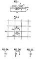
- FIG.1 is a cross-sectional view showing a capacitor of a memory cell of a BIC PROM
- FIG.2 is a circuit diagram showing an equivalent circuit of memory cells of the BIC PROM of Fig.
- FIGS.3A through 3C are equivalent circuit diagrams of a non-selected memory cell of the BIC PROM shown in FIG.2 before a write operation, during the write operation and after the write operation, respectively;
- FIGS.4A through 4C are equivalent circuit diagrams of a selected memory cell of the BIC PROM shown in FIG.2 before the write operation, during the write operation and after the write operation, respectively;
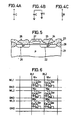
- FIG.5 is a cross-sectional view showing a memory cell of a BIC PROM embodying the present invention;
- FIG.6 is a circuit diagram showing an equivalent circuit of memory cells of a BIC PROM embodying the present invention;
- FIGS.7A through 7C are equivalent circuit diagrams of a non-selected memory cell of the BIC PROM shown in FIG.
- FIGS.8A through 8C are equivalent circuit diagrams of a selected memory cell of the BIC PROM shown in FIG. 6 before a write operation, during the write operation and after the write operation, respectively;
- FIG. 8A through 8C are equivalent circuit diagrams of a selected memory cell of the BIC PROM shown in FIG. 6 before a write operation, during the write operation and after the write operation, respectively;
- FIG. 8A through 8C are equivalent circuit diagrams of a selected memory cell of the BIC PROM shown in FIG. 6 before a write operation, during the write operation and after the write operation, respectively;
- FIG. 9 shows capacitances of an insulator layer and a depletion layer of the non-selected memory cell of the BIC PROM shown in FIG.6;
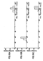
- FIGS.10A through 10C respectively show memory cell resistance distributions relating to a BIC PROM embodying the present invention;
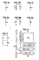
- FIG.11 is a system block diagram showing an example of circuit construction of a BIC PROM embodying the present invention;
- FIGS.12(A) through 12(I) are timing charts for explaining the operation of the BIC PROM shown in FIG.11;
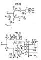
- FIG.13 is a system circuit diagram showing an example of a write circuit within a read/write circuit shown in FIG.11;
- FIG.14 is a circuit diagram showing an example of the concrete circuit construction of the write circuit shown in FIG.13;
- FIG.15 is a circuit diagram showing an example of a column decoder shown in FIG.11; and
- FIG.16 is a circuit diagram showing an example of a decoder shown in FIG.15.
- FIG.1 shows the cross section of a capacitor of a memory cell of a BIC PROM.
- the capacitor comprises a p-type silicon substrate 11, an n+-type impurity region 12 formed in a surface portion of the substrate 11, an insulator layer 13 formed on the substrate 11, an insulator layer 14 formed over a contact hole in the insulator layer 13, and an electrode wiring layer 15.
- the insulator layer 13 is made of phospho-silicate-glass (PSG)
- the electrode wiring layer 15 is made of aluminum (Al).
- FIG.2 shows the equivalent circuit of the memory cells of the BIC PROM of Fig. 1. For convenience' sake, only two memory cells are shown in FIG.2, but a plurality of such memory cells are arranged in a matrix arrangement.
- a memory cell M1 comprises an N-channel metal oxide semiconductor (MOS) FET Q1 and a capacitor C1
- a memory cell M2 comprises an N-channel MOS FET Q2 and a capacitor C2.
- Information is written into a selected memory cell by applying voltages to a word line and a bit line coupled thereto, and no information is written into a non-selected memory cell by applying no voltage to a word line coupled thereto.
- MOS metal oxide semiconductor
- FIGS.3A, 3B and 3C respectively show equivalent circuits of a non-selected memory cell before the write operation is performed, during the write operation and after the write operation. It may be seen that the memory cell is non-conductive when the insulator layer 14 of the capacitor thereof is not broken down.
- FIGS.4A, 4B and 4C respectively show equivalent circuits of a selected memory cell before the write operation is performed, during the write operation and after the write operation. It may be seen that the memory cell is conductive when the insulator 14 thereof is broken down, and in this case, the memory cell has a resistance R as shown in FIG.4C.
- the capacitance of the capacitor is denoted by C and the voltage applied to the capacitor is denoted by V.
- the non-conductive memory cell represents a data "0" and the conductive memory cell represents a data "1"
- the insulator layer 14 of the capacitor C1 of the memory cell M1 is broken down in the case where the data "1" is to be written into the memory cell M1.
- the memory cell having the capacitor with the broken down insulator layer represents the data "1”
- the memory cell having the capacitor with the normal insulator layer represents the data "0”.
- the data can be read out from the memory cell by applying a voltage to the insulator layer of the capacitor and amplifying a voltage which is read out of the memory cell. A current flows through the memory cell when the memory cell stores the data "1", but no current flows through the memory cell when the memory cell stores the data "0".
- a voltage having a level sufficient for breaking down the insulating layer is applied to the capacitor of the selected memory cell.
- the voltage applied to the memory cells is usually turned ON and OFF, so that the voltage is applied to only the capacitor of the selected memory cell and the voltage is not applied to the capacitor of the non-selected memory cells.
- a word line is coupled to a gate of the MOS FET and a bit line is grounded via the MOS FET and the capacitor.
- a word line WL is selected by applying a voltage to the word line WL, for example, the MOS FET Q2 of the memory cell M2 is turned ON.
- a write-in pulse voltage V is applied to a bit line BL
- the write-in pulse voltage is applied to the capacitor C2 of the memory cell M2 and the insulator layer of the capacitor C2 is broken down.
- the capacitor C2 becomes conductive as shown in FIG.4C and the data "1" is written into the memory cell M2.
- the MOS FET Q1 coupled to the bit line BL remains OFF because a word line coupled thereto is not selected. In other words, no voltage is applied to the word line which is coupled to the MOS FET Q1 of the memory cell M1, and the write-in pulse voltage will not be applied to the capacitor C1 of the memory cell M1. Therefore, the capacitor C1 remains non-conductive as shown in FIG.3C.
- the write-in pulse voltage for breaking down the insulating layer of the capacitor of the selected memory cell is applied to the capacitor via the MOS FET.
- an effective bias voltage applied to the insulator layer of capacitor the memory cell is as large as V G - V th even when the write-in pulse voltage is larger than V G - V th , where V G is the word line voltage and V th is the threshold voltage of the MOS FET of the memory cell. Therefore, the voltage V G V th must be larger than the breakdown voltage of the insulator layer of the capacitor of the memory cell.
- the MOS FET of the memory cell will become damaged if such a large word line voltage is applied to the gate electrode.
- FIG.5 shows the cross section of a memory cell of a BIC PROM embodying the present invention.
- the memory cell comprises a p-type silicon substrate 21, an n+-type impurity region 22 formed in a surface portion of the substrate 21, an insulator layer 23 formed on the substrate 21, an insulator layer 24 formed over a contact hole in the insulator layer 23, an electrode wiring layer 25, an n+-type source region 26 formed in the surface portion of the substrate 21, a gate layer 27, an electrode wiring layer 28 formed over a contact hole in the insulator layer 23, and a field oxide layer 29 for isolation.
- the insulator layer 23 is made of phospho-silicate-glass (PSG), the electrode wiring layers 25 and 28 are made of aluminum (Al), and the gate layer 27 is made of polysilicon.
- the gate layer 27 is coupled to the word line, the electrode wiring layer 25 is coupled to the bit line, and the electrode wiring layer 28 is grounded.
- the insulator layer 24 has a thickness of 50 ⁇ to 200 ⁇ .
- the insulator layer 24 covers a contact area which is formed on the PSG layer (insulator layer 23) to connect the drain diffusion region.
- the memory cell can be formed on the substrate 21 at a latter part of the production process.
- EPROM erasable PROM
- FIG.6 shows the equivalent circuit of the memory cells of a BIC PROM according to an embodiment of the present invention. For convenience' sake, only six memory cells are shown in FIG.6.
- a memory cell M11 comprises an N-channel MOS FET Q11 and a capacitor C11
- a memory cell M12 comprises an N-channel MOS FET Q12 and a capacitor C12.
- memory cells M21, M22, M31 and M32 comprise respective N-channel MOS FETs Q21, Q22, Q31 and Q32 and respective capacitors C21, C22, C31 and C32.
- a voltage is applied to a word line WL1 so as to turn ON the MOS FET Q11. Then, a write-in pulse voltage is applied to a bit line BL1. Unlike in the memory cells shown in FIG.2, the write-in pulse voltage from the bit line BL1 is applied directly to the capacitor C11 of the memory cell M11. As a result, the insulator layer of the capacitor C11 is broken down, and the memory cell M11 becomes conductive.
- FIGS.7A through 7C are equivalent circuit diagrams of the non-selected memory cell of the BIC PROM shown in FIG.6 before a write operation, during the write operation and after the write operation, respectively.
- this voltage is divided between the capacitor C21 (that is, the capacitance C0 of the insulator layer) and the capacitance C d of the depletion layer.
- the voltage which is actually applied to the insulator layer of the capacitor C21 becomes less than the insulator breakdown voltage, and the breakdown of the insulator layer of the capacitor C21 will not occur.
- the non-selected memory cell after the write operation has a capacitance C0' shown in FIG.7C which is equal to a capacitance of the series-connected capacitances C0 and C d .
- FIGS.8A through 8C are equivalent circuit diagrams of the selected memory cell of the BIC PROM shown in FIG.6 before a write operation, during the write operation and after the write operation, respectively.
- FIGS.8A through 8C when the insulator breakdown voltage is applied to the capacitor C11 of the selected memory cell M11, the insulator layer of this capacitor C11 will break down.
- the insulator layer of the non-selected memory cell will not break down even when applied with the voltage greater than the insulator breakdown voltage, and only the insulator layer of the selected memory cell is broken down. For this reason, it is possible to selectively write the information to the selected memory cell even when the insulator layers of the memory cells in the BIC PROM have a large insulator breakdown voltage.
- FIG.9 shows the capacitances of the insulator layer and the depletion layer of the non-selected memory cell.
- the insulator layer of the capacitor of the memory cell has the capacitance C0
- the depletion layer has the capacitance C d
- the voltage V0 is approximately 1/100 the voltage V1 because S1 and S0 are approximately equal to each other. This means that only a slight voltage, that is, virtually negligibly small voltage, is applied to the insulator layer of the capacitor and the breakdown of the insulator layer consequently does not occur. In other words, the information is positively written into only the selected memory cell and the information is positively prevented from being written into the non-selected memory cells.
- FIGS.10A through 10C Measured results of memory cell resistance distribution of a BIC PROM embodying the present invention before and after a write operation is performed are shown in FIGS.10A through 10C.
- FIG.10A shows the memory cell resistance distribution of the pre-programmed memory cells
- FIG.10B shows the memory cell resistance distribution of the selected memory cells after the write operation
- FIG.10C shows the memory cell resistance distribution of the non-selected memory cells after the write operation.
- the abscissa represents the memory cell resistance in 1/Gm ( ⁇ ) and the ordinate represents the percentage (%) of the measured memory cells.
- FIG.10B It may be seen from FIG.10B that the insulator layer of the capacitor of each selected memory cell is broken down after the write operation and that the resistance of the insulator layer has become low.
- FIG.10C it may be seen from FIG.10C that the insulator layer of the capacitor of each non-selected memory cell is not broken down and that the resistance of the insulator layer is high as in FIG.10A.
- the substrate is grounded, but it is not essential to ground the substrate, and the substrate may be biased by a constant voltage (for example, -2.5 V).
- a constant voltage is always applied to the insulator layer of the capacitor of the memory cell, however, the insulator layer will not break down with a sufficiently low substrate voltage.
- the insulator layer of the capacitor of the non-selected memory cell is prevented from breaking down by the series connection of the capacitances shown in FIG.9. Therefore, it is also possible in this case to satisfactorily write the information into the selected memory cell without breaking down the insulator layers of the non-selected memory cells.
- FIG.11 shows an example of a circuit construction of a BIC PROM embodying the present invention.
- the BIC PROM generally comprises a memory cell array 31, a row decoder 32, a column decoder 33, an address register 34 and a read/write circuit 35.
- the memory cell array 31 comprises the memory cells shown in FIG.6 arranged in a matrix arrangement, and is an 8-kbyte memory cell array, for example.
- the row decoder 32, the column decoder 33, the address register 34 and the read/write circuit 35 constitute a peripheral circuit of the memory cell array 31.
- a 13-bit address signal comprising bits A0 through A12
- the bits A0 through A4, A11 and A12 are supplied to the row decoder 32 while the bits A5 through A10 are supplied to the column decoder 32.
- a selected memory cell in the memory cell array 31 is designated by an output row address of the row decoder 32 and an output column address of the column decoder 33.
- a write operation a data to be written into the memory cell array 31 is supplied to the read/write circuit via the data bus 36, and an output data of the read/write circuit 35 is supplied to the memory cell array 31 and is written into the selected memory cell.
- a data is read out from the selected memory cell in the memory cell array 31 and is supplied to the data bus 36 via the read/write circuit 35.
- FIGS.12(A) through 12(I) show a write operation by referring to the time charts shown in FIGS.12(A) through 12(I).
- the memory cell array 31 comprises a 2 ⁇ 3 matrix arrangement of memory cells M11 through M32 as shown in FIG.6, and that the information is to be written into the selected memory cells M31, M11 and M22 in this sequence.
- FIG.12(A) shows a clock signal ⁇ having a period equal to the write cycle.
- An initializing operation is performed by applying a voltage Vc1 to each of the word lines WL1 through WL3 during a first half of each of write cycles T1, T2, T3 and the like as shown in FIGS.12(B) through 12(D) so that each of the nodes A11 through A32 are grounded.
- the word lines WL1 through WL3 are high and the nodes A11 through A32 are low during the first half of each write cycle.
- each of the bit lines BL1 and BL2 are low during the first half of each write cycle as shown in FIGS.12(E) and 12(F).
- a memory cell is selected by applying the voltage Vc1 to the the word line and applying a voltage Vc2 to the bit line which are coupled to the selected memory cell during a second half of the write cycle.
- the word line and the bit line coupled to the selected memory cell are made high during the second half of each write cycle.
- the voltage Vc1 is +5 V and the voltage Vc2 is +24 V.
- the memory cell M31 is the selected memory cell, the word line WL3 is high and the bit line BL1 is high during the second half of the write cycle T1 as shown in FIGS.12(D) and 12(E), and the insulator layer of the capacitor C31 of the memory cell M31 is broken down as shown in FIG.12(I).
- the non-selected memory cell M11 is also coupled to the bit line BL1 which is high during the second half of the write cycle T1, but since the word line WL1 coupled thereto remains low during the second half of the write cycle T1 as shown in FIG.12(B), the node A11 is in a floating state.
- the node A11 due to the capacitive coupling described before, the node A11 only rises to a voltage near the voltage Vc2 as shown in FIG.12(G), and a potential difference that would break down the insulator layer of the capacitor C11 of the memory cell M11 will not occur across the capacitor C11. Therefore, the insulator layer of the capacitor C11 of the memory cell M11 will not break down.
- the insulator layer of the capacitor C21 of the other non-selected memory cell M21 will also not break down for similar reasons.
- the word line WL1 and the bit line BL1 are made high during the second half of the write cycle T2 as shown in FIGS.12(B) and 12(D), and the insulator layer of the capacitor C11 of the selected memory cell M11 is broken down during the second half of the write cycle T2 as shown in FIG.12(G). Since the word line WL3 remains low during the second half of the write cycle T2, the insulator layer of the capacitor C31 of the non-selected memory cell M31 will not break down during the second half of the write cycle T2 as shown in FIG.12(I).
- the word line WL2 and the bit line BL2 are made high during the second half of the write cycle T3 as shown in FIGS.12(C) and 12(F), and the insulator layer of the capacitor C22 of the selected memory cell M22 is broken down during the second half of the write cycle T3.
- FIG.13 shows an example of a write circuit within the read/write circuit 35 shown in FIG.11.
- the write circuit comprises a 3-input NAND circuit 41, inverters 42 and 43, a 2-input NOR circuit 44, and N-channel transistors 45 and 46.
- a read/write control signal R /W, the clock signal ⁇ and a write-in data I are 1 respectively applied to input terminals 40a, 40b and 40c and are supplied to the NAND circuit 41.
- An output signal of the NAND circuit 41 is supplied to one input terminal of the NOR circuit 44 via the inverter 42 on one hand, and is supplied to the transistor 45 via the inverter 43 on the other.
- a read/write control signal R/ W is applied to an input terminal 40d and is supplied to the other input terminal of the NOR circuit 44.
- An output signal of the NOR circuit 44 is supplied to the transistor 46.
- An output signal obtained from a connection point of the transistors 45 and 46 is outputted via an output terminal 47 and is supplied to the column decoder 33 shown in FIG.11.
- the read/write control signal R /W is made high and the read/write control signal R/ W is made low.
- the clock signal ⁇ is high, the logic level of the write-in data I is outputted via the output terminal 47 in phase with the clock signal ⁇ .
- the read/write control signal R /W When performing a read operation, the read/write control signal R /W is made low and the read/write control signal R/ W is made high.
- the high-level read/write control signal R/ W is also applied to a terminal 48.
- an N-channel transistor 49 coupled to the output terminal 47 is turned ON during the read operation, and the read out data from the column decoder 33 is supplied to the data bus 36 via an inverter 50 and a terminal 51.
- FIG.14 shows an example of a concrete circuit construction of the write circuit shown in FIG.13.
- the write circuit comprises N-channel depletion type transistors Q2 and Q5, P-channel enhancement type transistors Q10, Q11, Q13 and Q17 through Q19, and N-channel enhancement type transistors Q1, Q3, Q4, Q6 through Q9, Q12 and Q14 through Q16.
- the transistors Q3 through Q7 have a high withstand voltage.
- the voltages Vc1 and Vc2 respectively are +5 V and + 25 V.
- the transistor Q15 When performing the write operation, the transistor Q15 is turned ON, the transistor Q19 is turned OFF, the transistor Q8 is turned OFF and the transistor Q10 is turned ON because the read/write control signal R /W is high and the read/write control signal R/ W is low.
- the clock signal ⁇ when the clock signal ⁇ is high, the logic level of the write-in data I is outputted via the output terminal 47 in phase with the clock signal ⁇ .
- the transistor Q7 In the case where the write-in data I is low (“0"), the transistor Q7 is turned ON and the transistor Q6 is turned OFF, and in this case, a low-level signal (ground level) is outputted via the output terminal 47.
- the transistor Q7 is turned OFF and the transistor Q6 is turned ON, and in this case, a high-level signal (Vc2) is outputted via the output terminal 47.
- Vc2 high-level signal
- the clock signal ⁇ is low
- the transistor Q7 is turned ON and the transistor Q6 is turned OFF, and a low-level signal (ground level) is outputted via the output terminal 47.
- the insulator layer of the capacitor of the selected memory cell having the MOS FET thereof turned ON breaks down when the high-level signal is outputted via the output terminal 47.
- the read/write control signal R /W is made low and the read/write control signal R/ W is made high.
- the transistor Q15 is turned OFF, the transistor Q19 is turned ON, the transistor Q8 is turned ON and the transistor Q10 is turned OFF. Since the transistors Q6 and Q7 are turned OFF in this case, the impedance of a signal line from the output terminal 47 to the column decoder 33 shown in FIG.11 becomes high. Therefore, it is possible to read out the data from the selected memory cell by use of a read circuit (not shown) which is coupled to the signal line.
- FIG.15 shows an example of the column decoder 33 shown in FIG.11.
- the column address comprises two bits.
- the column address comprises two bits B C1 and B C2
- one of four bit lines BL1 through BL4 can be selected.
- the signal from the output terminal 47 shown in FIGS.13 and 14 is supplied to a terminal 60.
- the column address bits B C1 and B C2 from the address register 34 shown in FIG.11 are applied to terminals 611 and 612.
- the bits B C1 and B C2 are supplied to decoders 62 through 65.
- Output signals of the decoders 62 through 65 turn ON N-channel transistors 661 through 664 coupled to the respective bit lines BL1 through BL4.
- the transistor 661 of the bit line BL1 is turned ON by the output signal of the decoder 62, and the signal from the terminal 60 is applied to the bit line BL1.
- FIG.16 shows an example of the decoder 62 shown in FIG.15. Since the decoders 63 through 65 are constructed similarly to the decoder 62, description will only be given with respect to the decoder 62.
- the decoder 62 comprises a P-channel transistor 71, N-channel transistors 72 through 74, and an inverter 75. A clock signal ⁇ p in phase synchronism with the clock signal ⁇ is applied to terminals 691 and 692. An output signal of the decoder 62 is obtained via the inverter 75 and a terminal 76 and is supplied to the transistor 661 of the bit line BL1 shown in FIG.15.
- each memory cell is constituted by a capacitor and a MOS FET, but it is possible to use a metal insulator semiconductor (MIS) FET instead of the MOS FET.
- MIS metal insulator semiconductor
- a circuit which is to be used is switched from a first circuit to a second circuit when the first circuit is defective.
- the memory cell described heretofore may be used as a switching element or device for carrying out the switching from the first circuit to the second circuit, by breaking down the insulator layer of the capacitor of the memory cell.
- a programmable semiconductor read only memory device comprises a memory cell array constituted by a plurality of memory cells arranged in a matrix arrangement.
- Each memory cell in the memory cell array comprises a transistor having a gate thereof coupled to a word line, and a capacitor comprising an insulator layer and having one terminal thereof coupled to a bit line and the other end thereof coupled to the transistor so that the capacitor is grounded via the transistor.
- the insulator layer of the capacitor of a selected memory cell breaks down thereby making the capacitor conductive when a specific word line and a specific bit line coupled to the selected memory cell are driven.
Landscapes
- Semiconductor Memories (AREA)
- Read Only Memory (AREA)
Claims (9)
- Programmierbare Halbleiter-Festwertspeichervorrichtung mit:
einem Speicherzellenarray, das durch eine Vielzahl von Speicherzellen gebildet ist, die in einer Matrixanordnung angeordnet sind, welche genannte Vielzahl von Speicherzellen mit entsprechenden Wortleitungen und entsprechenden Bitleitungen verbunden ist,
wobei die genannte Vielzahl von Speicherzellen in dem genannten Speicherzellenarray jeweils einen Transistor (Q11) umfaßt, von dem ein Gate mit einer Wortleitung (WL₁) gekoppelt ist, und einen Kondensator (C₁₁), der eine Isolatorschicht (24) umfaßt, welche genannte Isolatorschicht des Kondensators von nur einer ausgewählten Speicherzelle durchbricht, wodurch der Kondensator leitend wird, wenn eine spezifische Wortleitung und eine spezifische Bitleitung, die mit der genannten ausgewählten Speicherzelle verbunden sind, getrieben werden, dadurch gekennzeichnet, daß ein Anschluß des genannten Kondensators mit einer Bitleitung (BL₁) gekoppelt ist, und der andere Anschluß mit dem genannten Transistor gekoppelt ist, so daß der genannte Kondensator über den genannten Transistor geerdet ist. - Programmierbare Halbleiter-Festwertspeichervorrichtung nach Anspruch 1, bei der der genannte Transistor in jeder Speicherzelle ein Metallisolatorhalbleiter-Feldeffekttransistor ist.
- Programmierbare Halbleiter-Festwertspeichervorrichtung nach Anspruch 2, bei der der genannte Transistor in jeder Speicherzelle ein N-Kanal-Metallisolatorhalbleiter-Feldeffekttransistor ist, der genannte N-Kanal-Metallisolatorhalbleiter-Feldeffekttransistor ein Drain hat, das mit dem genannten anderen Ende des genannten Kondensators verbunden ist, und eine Source, die geerdet ist.
- Programmierbare Halbleiter-Festwertspeichervorrichtung nach Anspruch 1, bei der jede Speicherzelle ein Halbleitersubstrat umfaßt, erste und zweite Verunreinigungsbereiche, die in den Oberflächenabschnitten des genannten Halbleitersubstrats gebildet sind, eine erste Isolatorschicht, die auf dem genannten Halbleitersubstrat gebildet ist, wobei die genannte erste Isolatorschicht erste bzw. zweite Kontaktlöcher hat, die über den genannten ersten und zweiten Verunreinigungsbereichen gebildet sind, eine Gateschicht, die auf dem genannten Halbleitersubstrat gebildet ist, eine zweite Isolatorschicht, die über dem genannten ersten Kontaktloch in der genannten ersten Isolatorschicht gebildet ist, eine erste Verdrahtungsschicht, die über dem genannten zweiten Kontaktloch in der genannten ersten Isolatorschicht gebildet ist, und eine zweite Verdrahtungsschicht über der genannten zweiten Isolatorschicht gebildet ist, wobei die genannte erste Verdrahtungsschicht geerdet ist, die genannte zweite Verdrahtungsschicht mit der Bitleitung gekoppelt ist, die genannte Gateschicht mit der Wortleitung gekoppelt ist, und die genannte zweite Isolatorschicht die Isolatorschicht des genannten Kondensators bildet.
- Programmierbare Halbleiter-Festwertspeichervorrichtung nach Anspruch 4, bei der das genannte Halbleitersubstrat aus p-Typ-Silicium hergestellt ist, der genannte erste Verunreinigungsbereich ein n⁺-Typ-Verunreinigungsbereich ist, der ein Drain des Transistors bildet, der genannte zweite Verunreinigungsbereich ein n⁺-Typ-Verunreinigungsbereich ist, der eine Source des Transistors bildet.
- Programmierbare Halbleiter-Festwertspeichervorrichtung nach Anspruch 4 oder 5, bei der der genannte erste Verunreinigungsbereich in dem Transistor von einer nichtausgewählten Speicherzelle rückwärts vorgespannt ist, wodurch eine Verarmungsschicht gebildet wird, welche genannte Verarmungsschicht eine Kapazität hat, die kleiner als die Kapazität der genannten zweiten Isolatorschicht ist.
- Programmierbare Halbleiter-Festwertspeichervorrichtung nach einem der vorhergehenden Ansprüche, bei der nur die genannte spezifische Wortleitung, die mit der genannten ausgewählten Speicherzelle verbunden ist, getrieben wird, so daß der Transistor der genannten ausgewählten Speicherzelle EIN-geschaltet wird, die Wortleitungen, die mit nichtausgewählten Speicherzellen verbunden sind, nicht getrieben werden, so daß Transistoren der nichtausgewählten Speicherzellen AUS-geschaltet werden.
- Programmierbare Halbleiter-Festwertspeichervorrichtung nach einem der vorhergehenden Ansprüche, bei der der Kondensator in all den genannten vielen Speicherzellen in dem genannten Speicherzellenarray in einer ersten Hälfte eines Schreibzyklus entladen wird und nur der Transistor der ausgewählten Speicherzelle während einer zweiten Hälfte des genannten Schreibzyklus EIN-geschaltet wird.
- Programmierbare Halbleiter-Festwertspeichervorrichtung nach Anspruch 8, die ferner ein Adreßregister umfaßt, dem ein Adreßsignal zugeführt wird, einen Reihendecoder, dem ein Ausgang des genannten Adreßregisters zugeführt wird, um eine Reihenadresse der ausgewählten Speicherzelle innerhalb des genannten Speicherzellenarray durch Treiben der spezifischen Wortleitung, die mit der genannten ausgewählten Speicherzelle verbunden ist, zu designieren, einen Spaltendecoder, dem ein Ausgang des genannten Adreßregisters zugeführt wird, um eine Spaltenadresse der ausgewählten Speicherzelle innerhalb des genannten Speicherzellenarray durch Treiben der spezifischen Bitleitung, die mit der genannten ausgewählten Speicherzelle verbunden ist, zu designieren, und eine Lese/Schreib-Schaltung, um Daten, die in das genannte Speicherzellenarray geschrieben werden sollen, zu liefern und um Daten zu empfangen, die von dem genannten Speicherzellenarray ausgelesen werden, wobei die genannte Lese/Schreib-Schaltung eine Schreibschaltung zum Steuern des genannten Spaltendecoders umfaßt, alle der Wortleitungen in einer ersten Hälfte von jedem Schreibzyklus getrieben werden, die genannte Schreibschaltung den genannten Spaltendecoder so steuert, daß keine der Bitleitungen in der ersten Hälfte von jedem Schreibzyklus getrieben wird und nur die spezifische Bitleitung, die mit der ausgewählten Speicherzelle verbunden ist, während einer zweiten Hälfte von jedem Schreibzyklus getrieben wird.
Applications Claiming Priority (4)
| Application Number | Priority Date | Filing Date | Title |
|---|---|---|---|
| JP60195167A JPS6254899A (ja) | 1985-09-04 | 1985-09-04 | プログラマブルリ−ドオンリメモリおよびその書込方法 |
| JP195167/85 | 1985-09-04 | ||
| JP268547/85 | 1985-11-29 | ||
| JP60268547A JPS62128557A (ja) | 1985-11-29 | 1985-11-29 | 半導体記憶装置とその書込み方法 |
Publications (3)
| Publication Number | Publication Date |
|---|---|
| EP0213638A2 EP0213638A2 (de) | 1987-03-11 |
| EP0213638A3 EP0213638A3 (en) | 1989-02-15 |
| EP0213638B1 true EP0213638B1 (de) | 1991-07-03 |
Family
ID=26508960
Family Applications (1)
| Application Number | Title | Priority Date | Filing Date |
|---|---|---|---|
| EP86112185A Expired - Lifetime EP0213638B1 (de) | 1985-09-04 | 1986-09-03 | Programmierbare Halbleiterfestwertspeicheranordnung |
Country Status (4)
| Country | Link |
|---|---|
| US (1) | US4782466A (de) |
| EP (1) | EP0213638B1 (de) |
| KR (1) | KR900006155B1 (de) |
| DE (1) | DE3680050D1 (de) |
Families Citing this family (11)
| Publication number | Priority date | Publication date | Assignee | Title |
|---|---|---|---|---|
| US5367208A (en) | 1986-09-19 | 1994-11-22 | Actel Corporation | Reconfigurable programmable interconnect architecture |
| JPH01204298A (ja) * | 1988-02-08 | 1989-08-16 | Fujitsu Ltd | 半導体記憶回路 |
| NL8800846A (nl) * | 1988-04-05 | 1989-11-01 | Philips Nv | Geintegreerde schakeling met een programmeerbare cel. |
| US5257222A (en) * | 1992-01-14 | 1993-10-26 | Micron Technology, Inc. | Antifuse programming by transistor snap-back |
| US5781756A (en) * | 1994-04-01 | 1998-07-14 | Xilinx, Inc. | Programmable logic device with partially configurable memory cells and a method for configuration |
| DE19622275A1 (de) * | 1996-06-03 | 1997-12-04 | Siemens Ag | Redundanzkonzept für integrierte Speicher mit ROM-Speicherzellen |
| US5909049A (en) * | 1997-02-11 | 1999-06-01 | Actel Corporation | Antifuse programmed PROM cell |
| US5995409A (en) * | 1998-03-20 | 1999-11-30 | Silicon Aquarius, Inc. | Electrically-programmable read-only memory fabricated using a dynamic random access memory fabrication process and methods for programming same |
| FR2787922B1 (fr) * | 1998-12-23 | 2002-06-28 | St Microelectronics Sa | Cellule memoire a programmation unique en technologie cmos |
| DE10063683A1 (de) * | 2000-12-20 | 2002-03-14 | Infineon Technologies Ag | Schaltungsanordnung mit einer programmierbaren Verbindung |
| US7064973B2 (en) * | 2004-02-03 | 2006-06-20 | Klp International, Ltd. | Combination field programmable gate array allowing dynamic reprogrammability |
Family Cites Families (3)
| Publication number | Priority date | Publication date | Assignee | Title |
|---|---|---|---|---|
| JPS6057156B2 (ja) * | 1978-05-24 | 1985-12-13 | 株式会社日立製作所 | 半導体メモリ装置 |
| JPS5832789B2 (ja) * | 1980-07-18 | 1983-07-15 | 富士通株式会社 | 半導体メモリ |
| JPS5862893A (ja) * | 1981-10-09 | 1983-04-14 | Mitsubishi Electric Corp | Mosダイナミツクメモリ |
-
1986
- 1986-09-02 KR KR1019860007336A patent/KR900006155B1/ko not_active Expired
- 1986-09-02 US US06/902,675 patent/US4782466A/en not_active Expired - Lifetime
- 1986-09-03 EP EP86112185A patent/EP0213638B1/de not_active Expired - Lifetime
- 1986-09-03 DE DE8686112185T patent/DE3680050D1/de not_active Expired - Lifetime
Also Published As
| Publication number | Publication date |
|---|---|
| KR870003508A (ko) | 1987-04-17 |
| EP0213638A3 (en) | 1989-02-15 |
| DE3680050D1 (de) | 1991-08-08 |
| KR900006155B1 (ko) | 1990-08-24 |
| US4782466A (en) | 1988-11-01 |
| EP0213638A2 (de) | 1987-03-11 |
Similar Documents
| Publication | Publication Date | Title |
|---|---|---|
| US5675547A (en) | One time programmable read only memory programmed by destruction of insulating layer | |
| US6208549B1 (en) | One-time programmable poly-fuse circuit for implementing non-volatile functions in a standard sub 0.35 micron CMOS | |
| US6421293B1 (en) | One-time programmable memory cell in CMOS technology | |
| US5274593A (en) | High speed redundant rows and columns for semiconductor memories | |
| US5524093A (en) | Semiconductor memory device having an arrangement to reduce stresses on non-selected ferroelectric capacitors while achieving high integration | |
| KR910009438B1 (ko) | 반도체 메모리 | |
| US4543647A (en) | Electrically programmable non-volatile semiconductor memory device | |
| US4984054A (en) | Electric fuse for a redundancy circuit | |
| JPH0831564B2 (ja) | 半導体装置 | |
| US6177830B1 (en) | High voltage charge pump using standard sub 0.35 micron CMOS process | |
| GB1425766A (en) | Memory system | |
| US5699289A (en) | Power source circuit and wiring group for semiconductor memory device | |
| EP0213638B1 (de) | Programmierbare Halbleiterfestwertspeicheranordnung | |
| GB2144268A (en) | A semiconductor integrated circuit array which facilitates continuity testing | |
| US4554646A (en) | Semiconductor memory device | |
| US5844298A (en) | Method and apparatus for programming anti-fuses | |
| US7218142B2 (en) | Switch matrix circuit, logical operation circuit, and switch circuit | |
| US4794568A (en) | Redundancy circuit for use in a semiconductor memory device | |
| US5400344A (en) | Semiconductor device with function of testing insulation defect between bit lines and testing method therefor | |
| US6243294B1 (en) | Memory architecture for non-volatile storage using gate breakdown structure in standard sub 0.35 micron process | |
| JPH0361279B2 (de) | ||
| US4924438A (en) | Non-volatile semiconductor memory including a high voltage switching circuit | |
| US5528540A (en) | Redundant address decoder | |
| JPH0217875B2 (de) | ||
| US6812532B2 (en) | Semiconductor device with address programming circuit |
Legal Events
| Date | Code | Title | Description |
|---|---|---|---|
| PUAI | Public reference made under article 153(3) epc to a published international application that has entered the european phase |
Free format text: ORIGINAL CODE: 0009012 |
|
| AK | Designated contracting states |
Kind code of ref document: A2 Designated state(s): DE FR GB |
|
| PUAL | Search report despatched |
Free format text: ORIGINAL CODE: 0009013 |
|
| AK | Designated contracting states |
Kind code of ref document: A3 Designated state(s): DE FR GB |
|
| 17P | Request for examination filed |
Effective date: 19890322 |
|
| 17Q | First examination report despatched |
Effective date: 19901016 |
|
| GRAA | (expected) grant |
Free format text: ORIGINAL CODE: 0009210 |
|
| AK | Designated contracting states |
Kind code of ref document: B1 Designated state(s): DE FR GB |
|
| ET | Fr: translation filed | ||
| REF | Corresponds to: |
Ref document number: 3680050 Country of ref document: DE Date of ref document: 19910808 |
|
| PLBE | No opposition filed within time limit |
Free format text: ORIGINAL CODE: 0009261 |
|
| STAA | Information on the status of an ep patent application or granted ep patent |
Free format text: STATUS: NO OPPOSITION FILED WITHIN TIME LIMIT |
|
| 26N | No opposition filed | ||
| PGFP | Annual fee paid to national office [announced via postgrant information from national office to epo] |
Ref country code: FR Payment date: 19950911 Year of fee payment: 10 |
|
| PG25 | Lapsed in a contracting state [announced via postgrant information from national office to epo] |
Ref country code: FR Effective date: 19960930 |
|
| REG | Reference to a national code |
Ref country code: FR Ref legal event code: ST |
|
| REG | Reference to a national code |
Ref country code: FR Ref legal event code: ST |
|
| REG | Reference to a national code |
Ref country code: GB Ref legal event code: IF02 |
|
| PGFP | Annual fee paid to national office [announced via postgrant information from national office to epo] |
Ref country code: GB Payment date: 20030903 Year of fee payment: 18 |
|
| PGFP | Annual fee paid to national office [announced via postgrant information from national office to epo] |
Ref country code: DE Payment date: 20040902 Year of fee payment: 19 |
|
| PG25 | Lapsed in a contracting state [announced via postgrant information from national office to epo] |
Ref country code: GB Free format text: LAPSE BECAUSE OF NON-PAYMENT OF DUE FEES Effective date: 20040903 |
|
| GBPC | Gb: european patent ceased through non-payment of renewal fee |
Effective date: 20040903 |
|
| PG25 | Lapsed in a contracting state [announced via postgrant information from national office to epo] |
Ref country code: DE Free format text: LAPSE BECAUSE OF NON-PAYMENT OF DUE FEES Effective date: 20060401 |