EP0206063B1 - Method and apparatus for correcting printed circuit boards - Google Patents
Method and apparatus for correcting printed circuit boards Download PDFInfo
- Publication number
- EP0206063B1 EP0206063B1 EP86107771A EP86107771A EP0206063B1 EP 0206063 B1 EP0206063 B1 EP 0206063B1 EP 86107771 A EP86107771 A EP 86107771A EP 86107771 A EP86107771 A EP 86107771A EP 0206063 B1 EP0206063 B1 EP 0206063B1
- Authority
- EP
- European Patent Office
- Prior art keywords
- layer
- pad
- wire
- printed circuit
- heat
- Prior art date
- Legal status (The legal status is an assumption and is not a legal conclusion. Google has not performed a legal analysis and makes no representation as to the accuracy of the status listed.)
- Expired
Links
Images



Classifications
-
- B—PERFORMING OPERATIONS; TRANSPORTING
- B23—MACHINE TOOLS; METAL-WORKING NOT OTHERWISE PROVIDED FOR
- B23K—SOLDERING OR UNSOLDERING; WELDING; CLADDING OR PLATING BY SOLDERING OR WELDING; CUTTING BY APPLYING HEAT LOCALLY, e.g. FLAME CUTTING; WORKING BY LASER BEAM
- B23K11/00—Resistance welding; Severing by resistance heating
- B23K11/34—Preliminary treatment
-
- B—PERFORMING OPERATIONS; TRANSPORTING
- B23—MACHINE TOOLS; METAL-WORKING NOT OTHERWISE PROVIDED FOR
- B23K—SOLDERING OR UNSOLDERING; WELDING; CLADDING OR PLATING BY SOLDERING OR WELDING; CUTTING BY APPLYING HEAT LOCALLY, e.g. FLAME CUTTING; WORKING BY LASER BEAM
- B23K20/00—Non-electric welding by applying impact or other pressure, with or without the application of heat, e.g. cladding or plating
- B23K20/002—Non-electric welding by applying impact or other pressure, with or without the application of heat, e.g. cladding or plating specially adapted for particular articles or work
- B23K20/004—Wire welding
- B23K20/005—Capillary welding
-
- B—PERFORMING OPERATIONS; TRANSPORTING
- B23—MACHINE TOOLS; METAL-WORKING NOT OTHERWISE PROVIDED FOR
- B23K—SOLDERING OR UNSOLDERING; WELDING; CLADDING OR PLATING BY SOLDERING OR WELDING; CUTTING BY APPLYING HEAT LOCALLY, e.g. FLAME CUTTING; WORKING BY LASER BEAM
- B23K20/00—Non-electric welding by applying impact or other pressure, with or without the application of heat, e.g. cladding or plating
- B23K20/24—Preliminary treatment
-
- H—ELECTRICITY
- H05—ELECTRIC TECHNIQUES NOT OTHERWISE PROVIDED FOR
- H05K—PRINTED CIRCUITS; CASINGS OR CONSTRUCTIONAL DETAILS OF ELECTRIC APPARATUS; MANUFACTURE OF ASSEMBLAGES OF ELECTRICAL COMPONENTS
- H05K3/00—Apparatus or processes for manufacturing printed circuits
- H05K3/22—Secondary treatment of printed circuits
- H05K3/225—Correcting or repairing of printed circuits
-
- H—ELECTRICITY
- H05—ELECTRIC TECHNIQUES NOT OTHERWISE PROVIDED FOR
- H05K—PRINTED CIRCUITS; CASINGS OR CONSTRUCTIONAL DETAILS OF ELECTRIC APPARATUS; MANUFACTURE OF ASSEMBLAGES OF ELECTRICAL COMPONENTS
- H05K1/00—Printed circuits
- H05K1/02—Details
- H05K1/11—Printed elements for providing electric connections to or between printed circuits
- H05K1/115—Via connections; Lands around holes or via connections
- H05K1/116—Lands, clearance holes or other lay-out details concerning the surrounding of a via
-
- H—ELECTRICITY
- H05—ELECTRIC TECHNIQUES NOT OTHERWISE PROVIDED FOR
- H05K—PRINTED CIRCUITS; CASINGS OR CONSTRUCTIONAL DETAILS OF ELECTRIC APPARATUS; MANUFACTURE OF ASSEMBLAGES OF ELECTRICAL COMPONENTS
- H05K1/00—Printed circuits
- H05K1/02—Details
- H05K1/14—Structural association of two or more printed circuits
- H05K1/141—One or more single auxiliary printed circuits mounted on a main printed circuit, e.g. modules, adapters
-
- H—ELECTRICITY
- H05—ELECTRIC TECHNIQUES NOT OTHERWISE PROVIDED FOR
- H05K—PRINTED CIRCUITS; CASINGS OR CONSTRUCTIONAL DETAILS OF ELECTRIC APPARATUS; MANUFACTURE OF ASSEMBLAGES OF ELECTRICAL COMPONENTS
- H05K2201/00—Indexing scheme relating to printed circuits covered by H05K1/00
- H05K2201/09—Shape and layout
- H05K2201/09209—Shape and layout details of conductors
- H05K2201/095—Conductive through-holes or vias
- H05K2201/096—Vertically aligned vias, holes or stacked vias
-
- H—ELECTRICITY
- H05—ELECTRIC TECHNIQUES NOT OTHERWISE PROVIDED FOR
- H05K—PRINTED CIRCUITS; CASINGS OR CONSTRUCTIONAL DETAILS OF ELECTRIC APPARATUS; MANUFACTURE OF ASSEMBLAGES OF ELECTRICAL COMPONENTS
- H05K2201/00—Indexing scheme relating to printed circuits covered by H05K1/00
- H05K2201/10—Details of components or other objects attached to or integrated in a printed circuit board
- H05K2201/10227—Other objects, e.g. metallic pieces
- H05K2201/10287—Metal wires as connectors or conductors
-
- H—ELECTRICITY
- H05—ELECTRIC TECHNIQUES NOT OTHERWISE PROVIDED FOR
- H05K—PRINTED CIRCUITS; CASINGS OR CONSTRUCTIONAL DETAILS OF ELECTRIC APPARATUS; MANUFACTURE OF ASSEMBLAGES OF ELECTRICAL COMPONENTS
- H05K2203/00—Indexing scheme relating to apparatus or processes for manufacturing printed circuits covered by H05K3/00
- H05K2203/11—Treatments characterised by their effect, e.g. heating, cooling, roughening
- H05K2203/1115—Resistance heating, e.g. by current through the PCB conductors or through a metallic mask
-
- H—ELECTRICITY
- H05—ELECTRIC TECHNIQUES NOT OTHERWISE PROVIDED FOR
- H05K—PRINTED CIRCUITS; CASINGS OR CONSTRUCTIONAL DETAILS OF ELECTRIC APPARATUS; MANUFACTURE OF ASSEMBLAGES OF ELECTRICAL COMPONENTS
- H05K3/00—Apparatus or processes for manufacturing printed circuits
- H05K3/30—Assembling printed circuits with electric components, e.g. with resistors
- H05K3/303—Assembling printed circuits with electric components, e.g. with resistors with surface mounted components
- H05K3/305—Affixing by adhesive
-
- H—ELECTRICITY
- H05—ELECTRIC TECHNIQUES NOT OTHERWISE PROVIDED FOR
- H05K—PRINTED CIRCUITS; CASINGS OR CONSTRUCTIONAL DETAILS OF ELECTRIC APPARATUS; MANUFACTURE OF ASSEMBLAGES OF ELECTRICAL COMPONENTS
- H05K3/00—Apparatus or processes for manufacturing printed circuits
- H05K3/30—Assembling printed circuits with electric components, e.g. with resistors
- H05K3/32—Assembling printed circuits with electric components, e.g. with resistors electrically connecting electric components or wires to printed circuits
- H05K3/328—Assembling printed circuits with electric components, e.g. with resistors electrically connecting electric components or wires to printed circuits by welding
-
- H—ELECTRICITY
- H05—ELECTRIC TECHNIQUES NOT OTHERWISE PROVIDED FOR
- H05K—PRINTED CIRCUITS; CASINGS OR CONSTRUCTIONAL DETAILS OF ELECTRIC APPARATUS; MANUFACTURE OF ASSEMBLAGES OF ELECTRICAL COMPONENTS
- H05K3/00—Apparatus or processes for manufacturing printed circuits
- H05K3/30—Assembling printed circuits with electric components, e.g. with resistors
- H05K3/32—Assembling printed circuits with electric components, e.g. with resistors electrically connecting electric components or wires to printed circuits
- H05K3/34—Assembling printed circuits with electric components, e.g. with resistors electrically connecting electric components or wires to printed circuits by soldering
- H05K3/3447—Lead-in-hole components
-
- H—ELECTRICITY
- H05—ELECTRIC TECHNIQUES NOT OTHERWISE PROVIDED FOR
- H05K—PRINTED CIRCUITS; CASINGS OR CONSTRUCTIONAL DETAILS OF ELECTRIC APPARATUS; MANUFACTURE OF ASSEMBLAGES OF ELECTRICAL COMPONENTS
- H05K3/00—Apparatus or processes for manufacturing printed circuits
- H05K3/40—Forming printed elements for providing electric connections to or between printed circuits
- H05K3/4007—Surface contacts, e.g. bumps
- H05K3/4015—Surface contacts, e.g. bumps using auxiliary conductive elements, e.g. pieces of metal foil, metallic spheres
-
- H—ELECTRICITY
- H05—ELECTRIC TECHNIQUES NOT OTHERWISE PROVIDED FOR
- H05K—PRINTED CIRCUITS; CASINGS OR CONSTRUCTIONAL DETAILS OF ELECTRIC APPARATUS; MANUFACTURE OF ASSEMBLAGES OF ELECTRICAL COMPONENTS
- H05K3/00—Apparatus or processes for manufacturing printed circuits
- H05K3/40—Forming printed elements for providing electric connections to or between printed circuits
- H05K3/42—Plated through-holes or plated via connections
-
- H—ELECTRICITY
- H10—SEMICONDUCTOR DEVICES; ELECTRIC SOLID-STATE DEVICES NOT OTHERWISE PROVIDED FOR
- H10W—GENERIC PACKAGES, INTERCONNECTIONS, CONNECTORS OR OTHER CONSTRUCTIONAL DETAILS OF DEVICES COVERED BY CLASS H10
- H10W72/00—Interconnections or connectors in packages
- H10W72/071—Connecting or disconnecting
- H10W72/0711—Apparatus therefor
- H10W72/07141—Means for applying energy, e.g. ovens or lasers
-
- H—ELECTRICITY
- H10—SEMICONDUCTOR DEVICES; ELECTRIC SOLID-STATE DEVICES NOT OTHERWISE PROVIDED FOR
- H10W—GENERIC PACKAGES, INTERCONNECTIONS, CONNECTORS OR OTHER CONSTRUCTIONAL DETAILS OF DEVICES COVERED BY CLASS H10
- H10W72/00—Interconnections or connectors in packages
- H10W72/071—Connecting or disconnecting
- H10W72/0711—Apparatus therefor
- H10W72/07168—Means for storing or moving the material for the connector
-
- H—ELECTRICITY
- H10—SEMICONDUCTOR DEVICES; ELECTRIC SOLID-STATE DEVICES NOT OTHERWISE PROVIDED FOR
- H10W—GENERIC PACKAGES, INTERCONNECTIONS, CONNECTORS OR OTHER CONSTRUCTIONAL DETAILS OF DEVICES COVERED BY CLASS H10
- H10W72/00—Interconnections or connectors in packages
- H10W72/071—Connecting or disconnecting
- H10W72/075—Connecting or disconnecting of bond wires
- H10W72/07502—Connecting or disconnecting of bond wires using an auxiliary member
-
- H—ELECTRICITY
- H10—SEMICONDUCTOR DEVICES; ELECTRIC SOLID-STATE DEVICES NOT OTHERWISE PROVIDED FOR
- H10W—GENERIC PACKAGES, INTERCONNECTIONS, CONNECTORS OR OTHER CONSTRUCTIONAL DETAILS OF DEVICES COVERED BY CLASS H10
- H10W72/00—Interconnections or connectors in packages
- H10W72/071—Connecting or disconnecting
- H10W72/075—Connecting or disconnecting of bond wires
- H10W72/07521—Aligning
-
- H—ELECTRICITY
- H10—SEMICONDUCTOR DEVICES; ELECTRIC SOLID-STATE DEVICES NOT OTHERWISE PROVIDED FOR
- H10W—GENERIC PACKAGES, INTERCONNECTIONS, CONNECTORS OR OTHER CONSTRUCTIONAL DETAILS OF DEVICES COVERED BY CLASS H10
- H10W72/00—Interconnections or connectors in packages
- H10W72/071—Connecting or disconnecting
- H10W72/075—Connecting or disconnecting of bond wires
- H10W72/07551—Connecting or disconnecting of bond wires characterised by changes in properties of the bond wires during the connecting
- H10W72/07553—Connecting or disconnecting of bond wires characterised by changes in properties of the bond wires during the connecting changes in shapes
-
- H—ELECTRICITY
- H10—SEMICONDUCTOR DEVICES; ELECTRIC SOLID-STATE DEVICES NOT OTHERWISE PROVIDED FOR
- H10W—GENERIC PACKAGES, INTERCONNECTIONS, CONNECTORS OR OTHER CONSTRUCTIONAL DETAILS OF DEVICES COVERED BY CLASS H10
- H10W72/00—Interconnections or connectors in packages
- H10W72/50—Bond wires
- H10W72/531—Shapes of wire connectors
-
- H—ELECTRICITY
- H10—SEMICONDUCTOR DEVICES; ELECTRIC SOLID-STATE DEVICES NOT OTHERWISE PROVIDED FOR
- H10W—GENERIC PACKAGES, INTERCONNECTIONS, CONNECTORS OR OTHER CONSTRUCTIONAL DETAILS OF DEVICES COVERED BY CLASS H10
- H10W72/00—Interconnections or connectors in packages
- H10W72/50—Bond wires
- H10W72/531—Shapes of wire connectors
- H10W72/533—Cross-sectional shape
- H10W72/534—Cross-sectional shape being rectangular
-
- H—ELECTRICITY
- H10—SEMICONDUCTOR DEVICES; ELECTRIC SOLID-STATE DEVICES NOT OTHERWISE PROVIDED FOR
- H10W—GENERIC PACKAGES, INTERCONNECTIONS, CONNECTORS OR OTHER CONSTRUCTIONAL DETAILS OF DEVICES COVERED BY CLASS H10
- H10W72/00—Interconnections or connectors in packages
- H10W72/50—Bond wires
- H10W72/531—Shapes of wire connectors
- H10W72/5363—Shapes of wire connectors the connected ends being wedge-shaped
-
- H—ELECTRICITY
- H10—SEMICONDUCTOR DEVICES; ELECTRIC SOLID-STATE DEVICES NOT OTHERWISE PROVIDED FOR
- H10W—GENERIC PACKAGES, INTERCONNECTIONS, CONNECTORS OR OTHER CONSTRUCTIONAL DETAILS OF DEVICES COVERED BY CLASS H10
- H10W72/00—Interconnections or connectors in packages
- H10W72/50—Bond wires
- H10W72/531—Shapes of wire connectors
- H10W72/5366—Shapes of wire connectors the bond wires having kinks
-
- H—ELECTRICITY
- H10—SEMICONDUCTOR DEVICES; ELECTRIC SOLID-STATE DEVICES NOT OTHERWISE PROVIDED FOR
- H10W—GENERIC PACKAGES, INTERCONNECTIONS, CONNECTORS OR OTHER CONSTRUCTIONAL DETAILS OF DEVICES COVERED BY CLASS H10
- H10W72/00—Interconnections or connectors in packages
- H10W72/90—Bond pads, in general
- H10W72/951—Materials of bond pads
- H10W72/952—Materials of bond pads comprising metals or metalloids, e.g. PbSn, Ag or Cu
-
- Y—GENERAL TAGGING OF NEW TECHNOLOGICAL DEVELOPMENTS; GENERAL TAGGING OF CROSS-SECTIONAL TECHNOLOGIES SPANNING OVER SEVERAL SECTIONS OF THE IPC; TECHNICAL SUBJECTS COVERED BY FORMER USPC CROSS-REFERENCE ART COLLECTIONS [XRACs] AND DIGESTS
- Y10—TECHNICAL SUBJECTS COVERED BY FORMER USPC
- Y10T—TECHNICAL SUBJECTS COVERED BY FORMER US CLASSIFICATION
- Y10T156/00—Adhesive bonding and miscellaneous chemical manufacture
- Y10T156/10—Methods of surface bonding and/or assembly therefor
- Y10T156/1052—Methods of surface bonding and/or assembly therefor with cutting, punching, tearing or severing
-
- Y—GENERAL TAGGING OF NEW TECHNOLOGICAL DEVELOPMENTS; GENERAL TAGGING OF CROSS-SECTIONAL TECHNOLOGIES SPANNING OVER SEVERAL SECTIONS OF THE IPC; TECHNICAL SUBJECTS COVERED BY FORMER USPC CROSS-REFERENCE ART COLLECTIONS [XRACs] AND DIGESTS
- Y10—TECHNICAL SUBJECTS COVERED BY FORMER USPC
- Y10T—TECHNICAL SUBJECTS COVERED BY FORMER US CLASSIFICATION
- Y10T156/00—Adhesive bonding and miscellaneous chemical manufacture
- Y10T156/10—Methods of surface bonding and/or assembly therefor
- Y10T156/1089—Methods of surface bonding and/or assembly therefor of discrete laminae to single face of additional lamina
- Y10T156/1092—All laminae planar and face to face
-
- Y—GENERAL TAGGING OF NEW TECHNOLOGICAL DEVELOPMENTS; GENERAL TAGGING OF CROSS-SECTIONAL TECHNOLOGIES SPANNING OVER SEVERAL SECTIONS OF THE IPC; TECHNICAL SUBJECTS COVERED BY FORMER USPC CROSS-REFERENCE ART COLLECTIONS [XRACs] AND DIGESTS
- Y10—TECHNICAL SUBJECTS COVERED BY FORMER USPC
- Y10T—TECHNICAL SUBJECTS COVERED BY FORMER US CLASSIFICATION
- Y10T156/00—Adhesive bonding and miscellaneous chemical manufacture
- Y10T156/12—Surface bonding means and/or assembly means with cutting, punching, piercing, severing or tearing
- Y10T156/1317—Means feeding plural workpieces to be joined
- Y10T156/1322—Severing before bonding or assembling of parts
- Y10T156/1339—Delivering cut part in sequence to serially conveyed articles
-
- Y—GENERAL TAGGING OF NEW TECHNOLOGICAL DEVELOPMENTS; GENERAL TAGGING OF CROSS-SECTIONAL TECHNOLOGIES SPANNING OVER SEVERAL SECTIONS OF THE IPC; TECHNICAL SUBJECTS COVERED BY FORMER USPC CROSS-REFERENCE ART COLLECTIONS [XRACs] AND DIGESTS
- Y10—TECHNICAL SUBJECTS COVERED BY FORMER USPC
- Y10T—TECHNICAL SUBJECTS COVERED BY FORMER US CLASSIFICATION
- Y10T29/00—Metal working
- Y10T29/49—Method of mechanical manufacture
- Y10T29/49002—Electrical device making
- Y10T29/49117—Conductor or circuit manufacturing
- Y10T29/49124—On flat or curved insulated base, e.g., printed circuit, etc.
-
- Y—GENERAL TAGGING OF NEW TECHNOLOGICAL DEVELOPMENTS; GENERAL TAGGING OF CROSS-SECTIONAL TECHNOLOGIES SPANNING OVER SEVERAL SECTIONS OF THE IPC; TECHNICAL SUBJECTS COVERED BY FORMER USPC CROSS-REFERENCE ART COLLECTIONS [XRACs] AND DIGESTS
- Y10—TECHNICAL SUBJECTS COVERED BY FORMER USPC
- Y10T—TECHNICAL SUBJECTS COVERED BY FORMER US CLASSIFICATION
- Y10T29/00—Metal working
- Y10T29/49—Method of mechanical manufacture
- Y10T29/49002—Electrical device making
- Y10T29/49117—Conductor or circuit manufacturing
- Y10T29/49124—On flat or curved insulated base, e.g., printed circuit, etc.
- Y10T29/49147—Assembling terminal to base
- Y10T29/49149—Assembling terminal to base by metal fusion bonding
-
- Y—GENERAL TAGGING OF NEW TECHNOLOGICAL DEVELOPMENTS; GENERAL TAGGING OF CROSS-SECTIONAL TECHNOLOGIES SPANNING OVER SEVERAL SECTIONS OF THE IPC; TECHNICAL SUBJECTS COVERED BY FORMER USPC CROSS-REFERENCE ART COLLECTIONS [XRACs] AND DIGESTS
- Y10—TECHNICAL SUBJECTS COVERED BY FORMER USPC
- Y10T—TECHNICAL SUBJECTS COVERED BY FORMER US CLASSIFICATION
- Y10T29/00—Metal working
- Y10T29/49—Method of mechanical manufacture
- Y10T29/49002—Electrical device making
- Y10T29/49117—Conductor or circuit manufacturing
- Y10T29/49124—On flat or curved insulated base, e.g., printed circuit, etc.
- Y10T29/49155—Manufacturing circuit on or in base
- Y10T29/49162—Manufacturing circuit on or in base by using wire as conductive path
-
- Y—GENERAL TAGGING OF NEW TECHNOLOGICAL DEVELOPMENTS; GENERAL TAGGING OF CROSS-SECTIONAL TECHNOLOGIES SPANNING OVER SEVERAL SECTIONS OF THE IPC; TECHNICAL SUBJECTS COVERED BY FORMER USPC CROSS-REFERENCE ART COLLECTIONS [XRACs] AND DIGESTS
- Y10—TECHNICAL SUBJECTS COVERED BY FORMER USPC
- Y10T—TECHNICAL SUBJECTS COVERED BY FORMER US CLASSIFICATION
- Y10T29/00—Metal working
- Y10T29/49—Method of mechanical manufacture
- Y10T29/49002—Electrical device making
- Y10T29/49117—Conductor or circuit manufacturing
- Y10T29/49204—Contact or terminal manufacturing
-
- Y—GENERAL TAGGING OF NEW TECHNOLOGICAL DEVELOPMENTS; GENERAL TAGGING OF CROSS-SECTIONAL TECHNOLOGIES SPANNING OVER SEVERAL SECTIONS OF THE IPC; TECHNICAL SUBJECTS COVERED BY FORMER USPC CROSS-REFERENCE ART COLLECTIONS [XRACs] AND DIGESTS
- Y10—TECHNICAL SUBJECTS COVERED BY FORMER USPC
- Y10T—TECHNICAL SUBJECTS COVERED BY FORMER US CLASSIFICATION
- Y10T29/00—Metal working
- Y10T29/49—Method of mechanical manufacture
- Y10T29/49718—Repairing
- Y10T29/49732—Repairing by attaching repair preform, e.g., remaking, restoring, or patching
Definitions
- the present invention relates to a method and apparatus for enabling the modification or correction of printed circuit boards by adding interconnections to existing boards. It relates particularly to apparatus, herein called stitching-pads, for use on printed circuit boards to enable new electrical connections to be made. It relates further to apparatus and methods for fabricating such pads and for using such pads to provide bases on printed circuit boards to which connections may be welded in order to modify interconnections between existing electrical circuitry on such boards.
- a system currently on the market for making corrections to existing printed circuit boards by redoing the artwork is marketed by Additive Technology Corportion, a Massachusetts company.
- the printed circuit board is re-etched on a dielectric applied over existing circuitry to implement the corrections or engineering instructions. That method is expensive in that it is priced at several dollars per board with an initial set-up charge of several hundred dollars. It has been determined that that system is not cost effective for runs of fewer than 50,000 boards. The turn-around time is too long for many purposes, since it is approximately three weeks.
- FIG. 1 is a sectional view illustrating the application of this prior art system which involves three distinct steps, or procedures.
- step 1 an upper Tungsten electrode 26 is lowered until the teflon insulation 24 encasing nickel wire 22 is in contact with an etched pad of stainless steel.
- step 2 the upper electrode is advanced further against the teflon which breaks at its contact with the stainless steel as well as its contact with the Tungsten edge.
- step 3 a potential is applied across electrodes 26 and 28 causing the nickel wire and the stainless steel to be melted together to form a weld at 30 as a consequence of the excessive heat developed in the resistance at the nickel-stainless steel junction.
- the current flow between the aluminum electrode and the copper sheet causes little heat because of the high conductivity of both metals.
- the teflon flows back into the break at the top and thus is self- healing.
- the printed circuit boards according to the Augat system with its special boards have application primarily in the prototype stage.
- Augat markets a small wire stitching machine for use with its printed circuit boards for approximately two or three thousand dollars which permits placement and attachment of wires by hand.
- a more expensive semi-automatic machine is available utilizing an x-y table for positioning the printed circuit board.
- the positioning of the wire, the cutting of the wire, the routing of the wire, and other similar operations are performed manually. This system is objectionable for use in the correction of production runs because it requires the use of special boards and is labor intensive.
- the invention of this divisional patent relates a method as claimed for correcting existing standard printed circuit boards.
- the method uses pads which include one outer layer of adhesive material of a resin epoxy which will adhere to a surface, such as the face of a printed circuit board, when heat is applied to the pad. Once the epoxy resin has been bonded to a printed circuit board, heat can be applied again without disturbing the bond.
- the pads in- dude a layer of stainless steel forming all, or part, of the second outer layer of the pad to which suitable wire, such as nickle wire, can be welded, thus enabling connections to be completed through nickel wire between a succession of pads.
- a layer, or sheet, of copper may be located between the layer, or sheet, of resin epoxy and the layer, or sheet, of stainless steel in a preferred embodiment.
- a pad may be of a type called a "pivot pad” herein, consisting simply of layers of each material, with or without intermediate copper and other layers, to enable the epoxy face of the pad to be bonded to a printed circuit board while the opposite face of stainless steel is available for welding to suitable wire so that electrical connections can be made between pads.
- FIG. 1 a sectional view of a portion of a special printed circuit board according to the prior art is shown at 10.
- This board consists of a sandwich of four layers including two layers,' or sheets, of copper 12 and 14 separated by a layer of epoxy 16 with a sheet of stainless steel 18 affixed to one sheet of copper 14.
- a hole 20 through the printed circuit board is lined by a thin layer of copper 21 which is plated-through the hole for use in mounting electrical components by flow soldering and the like.
- an insulated wire In order to switch, or weld, an insulated wire to 'the stainless steel surface it is necessary to use wire of suitable materials and follow an effective procedure.
- a nickel wire 22, insulated by a layer of teflon 24, is placed in contact with the surface of the stainless steel sheet 18.
- a Tungsten electrode 26 is placed in contact with the teflon coating and force is applied with the view to rupturing the teflon coating where it contacts the stainless steel surface as well as where it contacts the Tungsten electrode.
- An electrode 28 made of highly conductive material, and preferably of aluminum, is placed against the surface of copper sheet 12.
- a low voltage source of electricity having high current capacity is applied across the electrodes 26, 28, causing the nickel wire and the surface of the stainless steel sheet to melt together to form a weld, as indicated by the dark spot at 30. It will be seen that the weld is formed due to the excessive heat developed in the area of the high resistance occuring at the junction of the nickel and stainless steel.
- the teflon coating has the characteristic property of flowing as it cools so that it flows back into the break to seal insulation over the point of the weld. Very little heat is developed at the junction of the aluminum electrode 28 and the copper sheet since this junction is of very low resistance.
- the pads are in the form of a sandwich construction having an adhesive layer in the form of a resin epoxy at 32 which is secured to a layer, or sheet, of epoxy material 34, which in a typical case would be of approximately 100 microns thickness. Attached to the epoxy material, on the side opposite the adhesive, is a layer of copper 36, approximately 15 microns in thickness, and attached to the copper is a stainless steel layer 38 which is approximately 100 microns in thickness.
- a plated through hole 40 is plated at 42 with an alloy of tin and lead (solder) over a copper layer 44.
- the plating in the holes is extended beyond the edges of the holes to overlap the face of the epoxy layer 34 and the face of the stainless steel layer 38 by approximately 0.015 inches.
- the invention encompasses pivot pads (page 2, Fig. 3) which are like the connecting pads but lack the plated-through holes.
- Connecting pads P1 such as are illustrated in Figs. 2A, 2B and pivot pads P2 (with no holes) are provided preferably in a ribbon or strip 46, as indicated in Fig. 3.
- connecting pads are grouped in pairs separated by one or two pivot pads. This arrangement was selected as convenient in a particular instance to facilitate cutting pads apart and mounting them on printed circuit boards by use of automatic equipment. It will be recognized, of course, that other arrangements of pivot pads and connecting pads are possible without departing from the spirit of the invention.
- the strip 46 may have the connecting pads and the pivot pads grouped in a different way so that connecting pads to enable connections to the board and pivot pads through which no connections to the board can be made are distributed exactly as needed over the board in a fashion to optimize the operation of apparatus according to the invention.
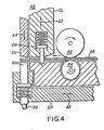
- the ribbon or strip-of-pads 46 is placed in a pad stamper 48, shown in partial section in Fig. 4, which positions the strip, clamps it, cuts it into individual pads and delivers the individual pads to a spoon holder SH.
- a strip 46 is positioned between pinch rollers R2, R4 of the pad stamper 48 which advances the strip-of-pads a predetermined distance which may be established by a human operator or by computer means.
- a centering needle CN may be inserted into the hole to better establish the position of the strip, impede further movement of the strip of positionable pads, and in cooperation with a pad clamper CL, which moves along the line marked by a two headed arrow A2, to clamp the strip in place and permit a pad of predetermined length to be severed from the strip by means of a cutter CU.
- a pivot pad is positioned under the centering pin or centering needle, and there is no hole to receive the centering pin, the centering pin remains in the withdrawn position and the pad clamper CL is moved, along the path indicated by the two headed arrow A2, into position against the strip 46 to secure the strip. While the strip is secured a pad of predetermined length is severed from the strip by means of the cutter CU moving along the path indicated by two headed arrow A4.
- the severed pad falls on a receiving member, or pad spoon, RM which is supported by the spoon holder SH which, in turn, is movable in the direction indicated by the associated two-headed arrow A6.
- the receiving member RM is coupled via tube 50 to a source of variable air pressure (not shown) so that it can either hold the pad or repel it.
- the pad is held in place by the receiving member RM making use of low air pressure.
- the holder SH is then moved in a direction along the horizontal indicated by arrow A6 to transport the pad to a position near a positioner PE as indicated in Fig. 5.
- air pressure is reversed through 50 to lift the pad off of the pad spoon RM and a vacuum is applied through 52 to lift the pad into contact with a pasting electrode PE.
- Pad holders at P4, P6 are then urged, by means not shown, into contact with the pad to hold it.
- a printed circuit board is then moved under the positioner containing the positionable pad with the movement of the printed circuit board being coarsely determined by an x-y table or other positioning means, and the fine positioning being accomplished with the use of a light beam and a four-quadrant sensor.
- the pad is a connecting pad (with a plated-through hole) the light beam is used to position the selected plated-through hole of the printed circuit board in line with the plated-through hole of the positionable pad to ensure the alignment of both plated-through holes.
- the pad is a pivot pad (with no plated-through hole) its position on the printed circuit board is determined with sufficient accuracy by the x-y table. In either case, the positionable pad is then affixed to the printed circuit board by utilizing pressure and two electrodes to cause a current flow. The flow of current develops heat in the positionable pad and causes the adhesive on the positionable pad to bond to the printed circuit board.
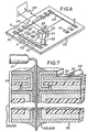
- Fig. 6 represents a printed circuit board positioned on an x-y table showing a plurality of connecting pads P1 and pivot pads P2 secured to the printed circuit board and interconnected by wires in accordance with further principles of the invention.
- the pads P1 and P2 are secured to the board when electricity is applied across two electrodes contacting one face of the pad and producing heat to fuze the adhesive epoxy to the printed circuit board.
- Fig. 7 illustrates a sectional view through a printed circuit board PC and an associated connecting pad, P1 on the board.
- a component C1 is shown in position where it has been inserted through and soldered into a plated-through hole which extends through the PC board and the pad.
- a nickel wire 22 is shown stitched (welded) to the stainless steel face of the pad. Other connections, not shown, may be completed to the solder on the lower side of the PC board using conventional flow-solder techniques.
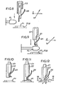
- FIG. 8-13 A preferred method, in accordance with the invention, for preparing wire for stitching (welding) and then stitching wire to positionable pads is shown in Figs. 8-13. This method includes the following steps:
- FIG. 16 represents an enlarged view of the tips of the electrodes E1, E2 with wire 24 extending over the end of E1 as they would appear from a vantage point along line 16-16 near the face of the pad in Fig. 12.
- a voltage of less than two volts and about 60 joules of energy is utilized for resistance welding.
- the energy to weld is dissipated through the electrodes by discharging a capacitor.
- the amount of energy is voltage and time dependent based upon the materials utilized.
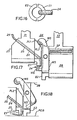
- Fig. 17 is an elevation showing details of a preferred stitching head of use in performing the operations set forth schematically in Figs. 8-15.
- a wire shooter WS serves the same purpose as the plunger PL of Fig. 9. It will be seen that a camming surface at PL1 engages a cam at PL2 which causes the wire shooter to move against a mechanical bias provided by a spring SP to bend the wire 24 as indicated.
- the wire 24 is fed through a needle hole 25 in the slab holder 27 and out through the electrode E1, as shown.
- a slab holder 29 supports the electrode E2 and the wire shooter WS.
- the slab holders in a preferred embodiment, are positioned by air pressure, systems operating through cylinders the shafts of which are indicated at 31 and 33.
- Fig. 18 is a representation of a portion of the stitching head showing the electrodes E1 and E2 in a position corresponding to that of Fig. 12 while stitching, or welding, is performed.
- the electrodes in both Fig. 18 and Fig. 12 occupy the relative positions, side-by-side, indicated in Fig. 16.
- the foregoing apparatus may be controlled by a microprocessor which relies on inputs from various actuators and sensors and is responsive to instructions stored in RAMS or ROMS.
- the microprocessor may also receive instructions from a datacom which is connected to a central processor and from a floppy disk.
- the software contained on the floppy disk is software unique to the printed circuit board being worked upon as it defines the exact location of wires, routings, etc.
- the positioning of the positionable pads and the wire stitching may be controlled manually using a joy stick or the joy stick may be utilized to create software to effect control.
- a second method may make use of a graphic terminal which utilizes the data for the printed circuit board and displays the actual artwork. By employing a cursor, the positionable pad and wire can be positioned, routed and terminated graphically. Once the operator is satisfied with the graphic corrections, such corrections, after being subject to certain review techniques and procedures, would be implemented in software.
- the positioning may also be automatically performed through use of a design file which compares the design with subsequent revisions; accordingly, the entire procedure can be automated.
- enhancements and improvements include replacing the x-y table with a robot control to provide a completely unattended machine.
- a further improvement is to provide a coating or abrasive tool for the purpose of removing or breaking existing connections on a printed circuit board, thereby permitting non-additive changes in the same operation.
Landscapes
- Engineering & Computer Science (AREA)
- Mechanical Engineering (AREA)
- Manufacturing & Machinery (AREA)
- Microelectronics & Electronic Packaging (AREA)
- Manufacturing Of Printed Wiring (AREA)
- Production Of Multi-Layered Print Wiring Board (AREA)
Applications Claiming Priority (2)
| Application Number | Priority Date | Filing Date | Title |
|---|---|---|---|
| GB8222359 | 1982-08-03 | ||
| GB08222359A GB2124835B (en) | 1982-08-03 | 1982-08-03 | Current printed circuit boards |
Related Parent Applications (2)
| Application Number | Title | Priority Date | Filing Date |
|---|---|---|---|
| EP83902435A Division EP0114857B1 (en) | 1982-08-03 | 1983-08-02 | Pad for correcting printed circuit boards and method of use thereof |
| EP83902435A Division-Into EP0114857B1 (en) | 1982-08-03 | 1983-08-02 | Pad for correcting printed circuit boards and method of use thereof |
Publications (3)
| Publication Number | Publication Date |
|---|---|
| EP0206063A2 EP0206063A2 (en) | 1986-12-30 |
| EP0206063A3 EP0206063A3 (en) | 1987-03-04 |
| EP0206063B1 true EP0206063B1 (en) | 1989-07-19 |
Family
ID=10532072
Family Applications (2)
| Application Number | Title | Priority Date | Filing Date |
|---|---|---|---|
| EP86107771A Expired EP0206063B1 (en) | 1982-08-03 | 1983-08-02 | Method and apparatus for correcting printed circuit boards |
| EP83902435A Expired EP0114857B1 (en) | 1982-08-03 | 1983-08-02 | Pad for correcting printed circuit boards and method of use thereof |
Family Applications After (1)
| Application Number | Title | Priority Date | Filing Date |
|---|---|---|---|
| EP83902435A Expired EP0114857B1 (en) | 1982-08-03 | 1983-08-02 | Pad for correcting printed circuit boards and method of use thereof |
Country Status (6)
| Country | Link |
|---|---|
| US (1) | US4654102A (OSRAM) |
| EP (2) | EP0206063B1 (OSRAM) |
| JP (1) | JPS5963792A (OSRAM) |
| DE (1) | DE3376187D1 (OSRAM) |
| GB (1) | GB2124835B (OSRAM) |
| WO (1) | WO1984000664A1 (OSRAM) |
Families Citing this family (11)
| Publication number | Priority date | Publication date | Assignee | Title |
|---|---|---|---|---|
| CA1322271C (en) * | 1987-02-25 | 1993-09-21 | Sho Masujima | Carrier tape for electronic circuit elements and method of manufacturing an electronic circuit element series |
| DE8711697U1 (de) * | 1987-08-28 | 1987-11-12 | Siemens AG, 1000 Berlin und 8000 München | Vorrichtung zum Ändern und/oder Reparieren von Flachbaugruppen bei Bestückung mit SMD-Bausteinen |
| WO1989006087A1 (en) * | 1987-12-18 | 1989-06-29 | Flowlyne (Uk) Limited | Improvements in or relating to the repair of electrical circuits |
| US5214250A (en) * | 1991-09-19 | 1993-05-25 | International Business Machines Corporation | Method of reworking circuit panels, and circuit panels reworked thereby |
| JP2856240B2 (ja) * | 1992-10-30 | 1999-02-10 | インターナショナル・ビジネス・マシーンズ・コーポレイション | プリント回路基板を再加工する方法 |
| CN1047408C (zh) * | 1995-09-11 | 1999-12-15 | 中国科学院金属研究所 | 一种激光化学气相沉积金刚石膜的方法 |
| US5794703A (en) * | 1996-07-03 | 1998-08-18 | Ctes, L.C. | Wellbore tractor and method of moving an item through a wellbore |
| US6181551B1 (en) | 1998-04-15 | 2001-01-30 | Dell Usa, L.P. | Pin soldering enhancement and method |
| US6907701B2 (en) * | 2001-06-07 | 2005-06-21 | Gary Edward Smith | Steel roofing panel support |
| US9409031B2 (en) | 2010-03-31 | 2016-08-09 | Medtronic, Inc. | Medical devices including flexible circuit bodies with exposed portions of circuit traces attached to electrical contacts of components |
| JP2015023187A (ja) * | 2013-07-19 | 2015-02-02 | イビデン株式会社 | 配線板および配線板の製造方法 |
Family Cites Families (22)
| Publication number | Priority date | Publication date | Assignee | Title |
|---|---|---|---|---|
| GB585186A (en) * | 1944-10-06 | 1947-01-31 | George Crawford Tyce | Improvements in and relating to the formation, reinforcement, or sealing of joints, for fibrous materials |
| DE1108754B (de) * | 1958-09-10 | 1961-06-15 | Siemens Ag | Verfahren und Vorrichtung zur Herstellung von Schaltungsplatten in Fernmelde-, insbesondere Fernsprech-anlagen |
| NL261568A (OSRAM) * | 1960-02-24 | |||
| US3234629A (en) * | 1962-06-14 | 1966-02-15 | Defiance Printed Circuit Corp | Method for producing printed circuits |
| FR1400933A (fr) * | 1964-07-11 | 1965-05-28 | Kupfer Asbest Co | Matériel conducteur pour circuits électriques et procédé pour la fabrication de plaques conductrices |
| GB1104274A (en) * | 1965-10-12 | 1968-02-21 | Plastic Coatings Ltd | Improvements in or relating to fusible adhesive compositions |
| US3536565A (en) * | 1967-09-14 | 1970-10-27 | Burroughs Corp | Method of making an electrical terminal board assembly |
| US3462540A (en) * | 1967-12-21 | 1969-08-19 | Bell Telephone Labor Inc | Method and apparatus for mounting,connecting and repairing stacked circuit boards |
| US3655818A (en) * | 1968-10-18 | 1972-04-11 | Minnesota Mining & Mfg | Particulate adhesive containing polyepoxides carboxylated butadiene-acrylonitrile copolymer and a urea derivative as a curing agent |
| US3680209A (en) * | 1969-05-07 | 1972-08-01 | Siemens Ag | Method of forming stacked circuit boards |
| US3827918A (en) * | 1972-05-25 | 1974-08-06 | Ibm | Electrical conductors with chromate solder barrier and method of forming |
| US3795047A (en) * | 1972-06-15 | 1974-03-05 | Ibm | Electrical interconnect structuring for laminate assemblies and fabricating methods therefor |
| US3786172A (en) * | 1972-12-07 | 1974-01-15 | Accra Point Arrays Corp | Printed circuit board method and apparatus |
| US3850711A (en) * | 1972-12-07 | 1974-11-26 | Accra Paint Arrays Corp | Method of forming printed circuit |
| DE2347217A1 (de) * | 1973-09-19 | 1975-03-27 | Siemens Ag | Verfahren zum durchkontaktieren eines beidseitig metallkaschierten basismaterials fuer gedruckte schaltungen |
| JPS5357481A (en) * | 1976-11-04 | 1978-05-24 | Canon Inc | Connecting process |
| GB1535820A (en) * | 1977-07-14 | 1978-12-13 | British Aircraft Corp Ltd | Electrically conductive connections |
| US4104109A (en) * | 1977-08-29 | 1978-08-01 | Bell Telephone Laboratories, Incorporated | Apparatus for bonding electrical contacts to printed wiring circuit boards |
| DE2925286A1 (de) * | 1979-06-22 | 1981-01-08 | Siemens Ag | Verfahren und schaltungsanordnung zum aendern von leiterplatten |
| DE3040460C2 (de) * | 1980-10-27 | 1982-12-16 | Siemens AG, 1000 Berlin und 8000 München | Elektronische Schaltung und Verfahren zu ihrer Herstellung |
| JPS57103386A (en) * | 1980-12-18 | 1982-06-26 | Tokyo Shibaura Electric Co | Method of modifying printed board |
| US4445952A (en) * | 1981-11-03 | 1984-05-01 | Trw Inc. | Apparatus and method for filling holes in a circuit board |
-
1982
- 1982-08-03 GB GB08222359A patent/GB2124835B/en not_active Expired
-
1983
- 1983-07-29 JP JP58140444A patent/JPS5963792A/ja active Granted
- 1983-08-02 DE DE8383902435T patent/DE3376187D1/de not_active Expired
- 1983-08-02 WO PCT/GB1983/000187 patent/WO1984000664A1/en not_active Ceased
- 1983-08-02 EP EP86107771A patent/EP0206063B1/en not_active Expired
- 1983-08-02 EP EP83902435A patent/EP0114857B1/en not_active Expired
-
1986
- 1986-05-20 US US06/867,908 patent/US4654102A/en not_active Expired - Fee Related
Also Published As
| Publication number | Publication date |
|---|---|
| EP0114857A1 (en) | 1984-08-08 |
| GB2124835A (en) | 1984-02-22 |
| US4654102A (en) | 1987-03-31 |
| GB2124835B (en) | 1986-04-30 |
| EP0206063A2 (en) | 1986-12-30 |
| DE3376187D1 (en) | 1988-05-05 |
| JPS5963792A (ja) | 1984-04-11 |
| EP0206063A3 (en) | 1987-03-04 |
| EP0114857B1 (en) | 1988-03-30 |
| JPH0479159B2 (OSRAM) | 1992-12-15 |
| WO1984000664A1 (en) | 1984-02-16 |
Similar Documents
| Publication | Publication Date | Title |
|---|---|---|
| KR100384796B1 (ko) | 도체를 접착시키기 위한 장치 및 방법 | |
| US4654102A (en) | Method for correcting printed circuit boards | |
| US5193732A (en) | Apparatus and methods for making simultaneous electrical connections | |
| GB1504252A (en) | Method and apparatus for obtaining electric interconnections of electric components on a base support | |
| JPH0620085B2 (ja) | 熔接装置 | |
| US4778556A (en) | Apparatus for correcting printed circuit boards | |
| US3626086A (en) | Wire-routing system | |
| EP0130498B1 (en) | Highly integrated universal tape bonding of semiconductor chips | |
| EP0243638B1 (en) | Microweld apparatus with an improved electrode tip design | |
| US3470612A (en) | Method of making multilayer circuit boards | |
| GB2155382A (en) | Stitch welding of wire to a printed circuit board | |
| GB2155368A (en) | Method and apparatus for correcting printed circuit boards | |
| JP2682006B2 (ja) | バンプ形成方法 | |
| JP2680461B2 (ja) | ディスクリート配線板及びその製造方法と製造装置 | |
| JPH11110925A (ja) | ディスク・ドライブ装置のアーム・アセンブリ及びこれの製造方法 | |
| JP2555915B2 (ja) | 金属突起物の形成方法,金属ろう材の供給方法およびそれらの治具 | |
| JP2603991B2 (ja) | 低抗溶接方法 | |
| JPH0661639A (ja) | ワイヤボンディングチップ構造 | |
| Gray et al. | Fixing Components to Printed Circuit Boards: A Review of the Conventional and More Advanced Methods | |
| JPS60182751A (ja) | 回路基板の配線パタ−ン形成方法 | |
| JPS6144495A (ja) | ワイヤ位置決め機構 | |
| KR20020068858A (ko) | 하면 접지부를 포함하는 비지에이용 비금속 리드 프레임 | |
| JPS5881578A (ja) | 抵抗溶接装置 | |
| JPH07297356A (ja) | 配線間の接合方法及び電子部品 | |
| JPH03183143A (ja) | 半導体装置及びその実装構造 |
Legal Events
| Date | Code | Title | Description |
|---|---|---|---|
| PUAI | Public reference made under article 153(3) epc to a published international application that has entered the european phase |
Free format text: ORIGINAL CODE: 0009012 |
|
| 17P | Request for examination filed |
Effective date: 19860613 |
|
| AC | Divisional application: reference to earlier application |
Ref document number: 114857 Country of ref document: EP |
|
| AK | Designated contracting states |
Kind code of ref document: A2 Designated state(s): BE DE FR NL SE |
|
| PUAL | Search report despatched |
Free format text: ORIGINAL CODE: 0009013 |
|
| AK | Designated contracting states |
Kind code of ref document: A3 Designated state(s): BE DE FR NL SE |
|
| RAP1 | Party data changed (applicant data changed or rights of an application transferred) |
Owner name: BURROUGHS MACHINES LIMITED Owner name: UNISYS CORPORATION |
|
| RAP1 | Party data changed (applicant data changed or rights of an application transferred) |
Owner name: UNISYS LIMITED Owner name: UNISYS CORPORATION |
|
| 17Q | First examination report despatched |
Effective date: 19881206 |
|
| GRAA | (expected) grant |
Free format text: ORIGINAL CODE: 0009210 |
|
| AC | Divisional application: reference to earlier application |
Ref document number: 114857 Country of ref document: EP |
|
| AK | Designated contracting states |
Kind code of ref document: B1 Designated state(s): BE DE FR NL SE |
|
| REF | Corresponds to: |
Ref document number: 3380247 Country of ref document: DE Date of ref document: 19890824 |
|
| ET | Fr: translation filed | ||
| PLBE | No opposition filed within time limit |
Free format text: ORIGINAL CODE: 0009261 |
|
| STAA | Information on the status of an ep patent application or granted ep patent |
Free format text: STATUS: NO OPPOSITION FILED WITHIN TIME LIMIT |
|
| 26N | No opposition filed | ||
| PGFP | Annual fee paid to national office [announced via postgrant information from national office to epo] |
Ref country code: BE Payment date: 19920909 Year of fee payment: 10 |
|
| PGFP | Annual fee paid to national office [announced via postgrant information from national office to epo] |
Ref country code: SE Payment date: 19930719 Year of fee payment: 11 |
|
| PGFP | Annual fee paid to national office [announced via postgrant information from national office to epo] |
Ref country code: FR Payment date: 19930808 Year of fee payment: 11 |
|
| PGFP | Annual fee paid to national office [announced via postgrant information from national office to epo] |
Ref country code: DE Payment date: 19930825 Year of fee payment: 11 |
|
| PG25 | Lapsed in a contracting state [announced via postgrant information from national office to epo] |
Ref country code: BE Effective date: 19930831 |
|
| PGFP | Annual fee paid to national office [announced via postgrant information from national office to epo] |
Ref country code: NL Payment date: 19930831 Year of fee payment: 11 |
|
| BERE | Be: lapsed |
Owner name: UNISYS LTD Effective date: 19930831 Owner name: UNISYS CORP. Effective date: 19930831 |
|
| PG25 | Lapsed in a contracting state [announced via postgrant information from national office to epo] |
Ref country code: SE Effective date: 19940803 |
|
| EAL | Se: european patent in force in sweden |
Ref document number: 86107771.7 |
|
| PG25 | Lapsed in a contracting state [announced via postgrant information from national office to epo] |
Ref country code: NL Effective date: 19950301 |
|
| NLV4 | Nl: lapsed or anulled due to non-payment of the annual fee | ||
| PG25 | Lapsed in a contracting state [announced via postgrant information from national office to epo] |
Ref country code: FR Effective date: 19950428 |
|
| PG25 | Lapsed in a contracting state [announced via postgrant information from national office to epo] |
Ref country code: DE Effective date: 19950503 |
|
| EUG | Se: european patent has lapsed |
Ref document number: 86107771.7 |
|
| REG | Reference to a national code |
Ref country code: FR Ref legal event code: ST |