EP0200452B1 - Ecran électromagnétique transparent - Google Patents
Ecran électromagnétique transparent Download PDFInfo
- Publication number
- EP0200452B1 EP0200452B1 EP86302982A EP86302982A EP0200452B1 EP 0200452 B1 EP0200452 B1 EP 0200452B1 EP 86302982 A EP86302982 A EP 86302982A EP 86302982 A EP86302982 A EP 86302982A EP 0200452 B1 EP0200452 B1 EP 0200452B1
- Authority
- EP
- European Patent Office
- Prior art keywords
- layer
- light
- plate
- hard coating
- base plate
- Prior art date
- Legal status (The legal status is an assumption and is not a legal conclusion. Google has not performed a legal analysis and makes no representation as to the accuracy of the status listed.)
- Expired - Lifetime
Links
Images

Classifications
-
- H—ELECTRICITY
- H01—ELECTRIC ELEMENTS
- H01J—ELECTRIC DISCHARGE TUBES OR DISCHARGE LAMPS
- H01J29/00—Details of cathode-ray tubes or of electron-beam tubes of the types covered by group H01J31/00
- H01J29/86—Vessels; Containers; Vacuum locks
- H01J29/89—Optical or photographic arrangements structurally combined or co-operating with the vessel
- H01J29/896—Anti-reflection means, e.g. eliminating glare due to ambient light
-
- H—ELECTRICITY
- H01—ELECTRIC ELEMENTS
- H01J—ELECTRIC DISCHARGE TUBES OR DISCHARGE LAMPS
- H01J29/00—Details of cathode-ray tubes or of electron-beam tubes of the types covered by group H01J31/00
- H01J29/86—Vessels; Containers; Vacuum locks
- H01J29/867—Means associated with the outside of the vessel for shielding, e.g. magnetic shields
- H01J29/868—Screens covering the input or output face of the vessel, e.g. transparent anti-static coatings, X-ray absorbing layers
-
- H—ELECTRICITY
- H01—ELECTRIC ELEMENTS
- H01J—ELECTRIC DISCHARGE TUBES OR DISCHARGE LAMPS
- H01J2229/00—Details of cathode ray tubes or electron beam tubes
- H01J2229/89—Optical components associated with the vessel
- H01J2229/8913—Anti-reflection, anti-glare, viewing angle and contrast improving treatments or devices
- H01J2229/8918—Anti-reflection, anti-glare, viewing angle and contrast improving treatments or devices by using interference effects
-
- H—ELECTRICITY
- H01—ELECTRIC ELEMENTS
- H01J—ELECTRIC DISCHARGE TUBES OR DISCHARGE LAMPS
- H01J2229/00—Details of cathode ray tubes or electron beam tubes
- H01J2229/89—Optical components associated with the vessel
- H01J2229/8913—Anti-reflection, anti-glare, viewing angle and contrast improving treatments or devices
- H01J2229/8922—Apparatus attached to vessel and not integral therewith
Definitions
- the present invention relates to a light-transmissible plastic plate which shields electromagnetic waves. More particularly, the present invention relates to a light-transmissible plate capable of effectively shielding deleterious electromagnetic waves which are generated from a display or a Braun tube etc. Moreover, the present invention relates to a light-transmissible plate having durability and the function of reducing reflection.
- One of the improvements is a method of covering the equipment which generates electromagnetic waves with electroconductive material such as a metal.
- a cloth capable of shielding electromagnetic waves and an "Eyesaver” (the trade name of a product of Chori Kabushiki Kaisha, a Japanese company) are known.
- the cloth is constructed by adhering carbon onto a fiber with small diameter and then weaving the fiber to form a meshed structure, and the cloth is applied on equipment which generates electromagnetic waves.
- "Eyesaver” is constructed of glass sheets and metal wire positioned between the sheets.
- a method of forming an evaporation coating layer of electroconductive material on a glass plate is also known. Such a method is disclosed, for example, in Japanese Patent Publication No. SHO 49-18447.
- GB-A-2121075 discloses a method of forming a heatwave shielding lamination coating of electroconductive material on a glass window using the DC magnetron sputtering method. In this method a car window pane is heated to 370°C in an atmosphere at a pressure of 3 x 10 ⁇ 3 Torr.
- the lamination coating includes layers of the same refractive index at visible wavelengths but different refractive indices at infrared wavelengths.
- the base plate is liable to soften or to melt, and is liable to be damaged at the surface. Therefore, the method cannot be applied for manufacturing a light-transmissible plastic plate.
- US-A-4422721 describes the application to glass of anti-reflection coatings each comprising a layer of low refractive index carrying an electroconductive layer of high refractive index.
- EP-A-0145210 describes anti-reflection optical coatings provided on an anti-reflective panel of unspecified material and bonded to the viewing screen of a cathode ray tube.
- the anti-reflection optical coatings each include an electroconductive layer and a free surface layer of a material having a refractive index lower than that of the electroconductive layer.
- SHO 59-48702, SHO 59-78301 and SHO 59-78304 disclose a method of providing anti-reflection coatings wherein a hard coating film comprising a polyorganosilane or a hardened film comprising an epoxy resin is formed on a plastic base plate and then an anti-reflection film comprising inorganic material is coated on the above hard coating layer.
- Japanese Patent Publication No. SHO 56-113101 discloses a structure wherein an anti-reflection film comprising a plurality of oxide compound layers is provided on a plastic base plate. The structure has high hardness at the surface and a satisfactory anti-reflection function, but adhesion between the base plate and the film, heat resistance, shock resistance, hot water resistance and weather resistance thereof are not satisfactory.
- Japanese Patent Publication Nos. SHO 45-6193, SHO 59-48702, SHO 59-78301 and SHO 59-78304 disclose other structures including other anti-reflection films, but the adhesion between the base plate and the anti-reflection film in these structures is also unsatisfactory, and the surfaces of anti-reflection films are liable to be damaged. Moreover, the plates are liable to be damaged by water or alcohol, and the structures have adhesion problems between the base plate and the film after dipping the plate into hot water and also in severe weather.
- the present invention seeks to provide a light-transmissible plate which can shield electromagnetic waves wherein an electroconductive layer is coated on a base plate, even if the base plate is constructed of a plastic material.
- the present invention in one of its aspects also seeks to provide a technology wherein hardness at a surface of the light-transmissible plate can be increased.
- the invention seeks to provide a technology wherein the light-transmissible plate can also have a function of anti-reflection.
- the present invention seeks to provide a light-transmissible plate which includes an anti-reflection film having excellent physical properties in various respects.
- a light-transmissible plate capable of transmitting visible light and yet shielding electromagnetic waves generated by electronic equipment and having: a transparent plastic base plate; on a surface of the transparent base plate, a first hard coating layer having scratch resistance; on a surface of the hard coating layer remote from the transparent plastic base plate, an electroconductive layer, which electroconductive layer contains indium oxide and tin oxide; on a surface of the electroconductive layer remote from the transparent plastic base plate, a layer having a refractive index in the visible light region which is lower than that of said electroconductive layer; on a surface of the transparent plastic base plate which is to face a viewer, a second hard coating layer; and on a surface of the second hard coating layer remote from the transparent plastic base plate, an antireflective coating, which antireflective coating consists of a plurality of layers, wherein the first hard coating layer on which is disposed the electroconductive layer is disposed on a surface of the transparent base plate which is to face the source of visible light, being opposite to the surface
- the invention provides (i) an electronic device having a source of visible light and including the above light transmissible plate, and (ii) the use, for the transmission of light from a light source of an electronic device while at the same time shielding electromagnetic waves from the electronic device, of the above light transmissible plate.
- the invention provides a method of preparing the above plate, which method comprises the steps of
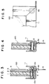
- FIG. 1 is a sectional view of a light-transmissible plate having the function of shielding electromagnetic waves and the function of resisting static charge according to one embodiment of the present invention.
- Hard coating layer 2 is provided on one surface of the transparent base plate 1, and the hard coating layer 2 has scratch resistance.
- Electroconductive layer 3 is provided on a surface of the hard coating layer 2.
- Layer 4 is provided on a surface of the electroconductive layer 3, and layer 4 has a lower refractive index than the refractive index of the electroconductive layer 3.
- Numeral 5 refers to a portion of an exposed surface of electroconductive layer 3.
- Light-transmissible plate 100 is disposed so as to direct a surface having electroconductive layer 3 toward a surface generating picture image, for example, a surface of a cathode-ray tube.
- FIG. 2 is a plan view of the light-transmissible plate 100 in FIG. 1.
- Exposed surface 5 of electroconductive layer 3 may be formed either along the entire periphery of the light-transmissible plate 100, or along only a part of the periphery.
- a metal frame (not shown) is provided around the plate 100 so as to contact with electroconductive layer 3, or an earthing wire 6 is connected to the electroconductive layer 3.
- the earthing wire 6 is connected desirably to a corner of electroconductive layer 3.
- FIG. 3 - 7 show preferred embodiments according to the present invention in relation to connecting an earthing wire.
- hole 9 is provided through the light-transmissible plate 100, and an earthing wire 15 is connected thereto via metal fitting piece 6a.
- metal fitting piece 6a is fixed by a fixing means, for example, set screw 10a and nut 10b (FIG.3), or a caulking piece 8 (FIG. 4). Then the portion of the connection is covered by a plastic cover 11.
- FIG. 5 shows an embodiment wherein metal fitting piece 6a is fixed nearly parallel to light-transmissible plate 100 in plastic cover 11.
- FIG. 6 shows an embodiment wherein helical insert 12 is fitted into hole 9 and earthing wire 15 is fixed by screw 13 via metal fitting piece 6a.
- providing a hole 11a on the cover 11 facilitates removing the screw 13, and the structure is convenient for removing light-transmissible plate 100 from equipment or cleaning the plate 100.
- FIG. 7 shows an embodiment wherein earthing wire 15 is connected to the plate 100 via adjuster 14a and 14b.
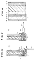
- FIG. 8 is a partial sectional view of a light-transmissible plate having an anti-reflection film constituted by a plurality of layers according to a second embodiment of the present invention.
- hard coating layer 2 On one surface of transparent plastic base plate 1, hard coating layer 2, electroconductive layer 3 and layer 4 having a lower refractive index than the refractive index of electroconductive layer 3 are provided, and on another surface of base plate 1, hard coating layer 2' having scratch resistance and anti-reflection film 20 are provided.
- Anti-reflection film 20 is constructed of No. 1 layer 21, No. 2 layer 22, No. 3 layer 23 and No. 4 layer 24.
- a first hard coating layer having scratch resistance is provided on a first surface of a transparent plastic base plate.
- a plastic constituting the base plate may be any conventional plastic.
- the transparent base plate means any plastic plate capable of transmitting light. In the case where a light-transmissible plate is used for a display of a word processor etc., it is desirable to apply a base plate set to the transmittance of visible rays of 25 - 70% by its own color or dyeing. Fatigue of the eyes of an operator is reduced by the above restriction.
- the hard coating layer having scratch resistance means a coating layer having high hardness, for example, a layer including polyorganosiloxane, silica or alumina, or a coating layer constructed of a hardening paint, for example, an acrylic paint.
- the hard coating layer consists of a polyorganosiloxane which is produced by heat-condensing after coating methyltrimethoxysilane and vinyltriethoxysilane or after coating a hydrolysis compound thereof.
- a desirable film thickness of the hard coating layer is in the range of about 1 - 10 ⁇ m.
- the hard coating layer including the acrylic is constructed of, for example, a compound crosslinked with an acrylic compound and an ester compound.
- the acrylic compound is constructed of, for example, methacrylic acid and the ester compound is constructed of, for example, an ester compound produced from an ester and a polyfunctional glycol, for example, pentaerythritol or glycerin.
- an electroconductive layer is provided on a surface of the hard coating layer.
- Any material having electroconductivity and capable of transmitting light can be used for the electroconductive layer, but preferably the layer is constructed of a mixture with indium oxide (In2O3) and tin oxide (SnO2), referred to hereinafter as "ITO".
- ITO has high electroconductivity, can shield electromagnetic waves effectively and can transmit visible rays.
- a film thickness of the "ITO” layer may be any thickness as long as the layer can satisfy the above functions.
- a desirable thickness is in the range of 100 - 3000 ⁇ (10-300nm) If a thickness of more than 300 nm is utilized, cracking is liable to occur.
- the "ITO” layer can be coated by sputtering.
- the "ITO” layer is formed by evaporation coating using plasma due to high-frequency electric discharge in an atmosphere of oxygen and in a temperature condition of less than 150°C, with the assistance of an ion gun.
- a layer having a lower refractive index than the refractive index of the electroconductive layer is provided on the surface of the electroconductive layer.
- the refractive index of the layer is high.
- the refractive index of the "ITO" layer is about 2.0.
- the layer having a low refractive index may be any conventional layer of low refractive index, but desirably the layer is a layer including inorganic silica.
- the layer including inorganic silica can be formed by sputtering the silica or by vacuum evaporation coating of the silica.
- the film thickness of the layer may be any thickness as long as the layer can appropriately prevent reflection.
- the first hard coating layer, the electroconductive layer and the layer having the low refractive index are provided on the first surface of the base plate, while on a second surface of the base plate opposite the first surface at least a second hard coating layer is provided and on this second hard coating layer an anti-reflection coating is provided.
- the anti-reflection coating is a film composed of a plurality of layers which in turn may be referred to as a No. 1 layer, No. 2 layer, No. 3 layer and a No. 4 layer.
- the No. 1 layer is provided on the surface of the second hard coating layer.
- the principal ingredient of the No. 1 layer is zirconium oxide.
- the No. 2 layer is provided on the surface of the No. 1 layer, and the principal ingredient of the No. 2 layer is silicon dioxide.
- the No. 1 layer serves as a binder between the hard coating layer and the No. 2 layer, and the strength of both adhesions between the hard coating layer and the No. 1 layer and between the No. 1 layer and the No. 2 layer is increased.
- the No. 1 layer serves as a binder between the hard coating layer and the No. 2 layer, and the strength of both adhesions between the hard coating layer and the No. 1 layer and between the No. 1 layer and the No. 2 layer is increased.
- the No. 1 layer serves as
- the equivalent film can be a film having a middle refractive index, ie a refractive index between that of the No. 3 layer having a high refractive index and that of the No. 4 layer having a low refractive index.
- the No. 3 layer is provided on a surface of the No. 2 layer, and the principal ingredient of the No. 3 layer is titanium oxide.
- the No. 4 layer is provided on a surface of the No. 3 layer, and the principal ingredient of the No. 4 layer is silicon dioxide.
- the film equivalent to No. 1 layer and No. 2 layer and having the middle refractive index, the No. 3 layer having the high index and the No. 4 layer having the low index, constitute the anti-reflection film as a whole, with the film having the excellent function of preventing reflection.
- the above anti-reflection film can be coated by vacuum evaporation or sputtering. Vacuum evaporation is better than sputtering. The assistance of an ion beam may be utilized for forming the film. Titanium oxide can be added into the No. 1 layer including zirconium oxide as long as the effect desired for a light transmissible plate of the present invention is not reduced. In the same manner, Ta2O5 can be added to the No. 3 layer including titanium oxide.
- the thickness of the anti-reflection film may be any thickness as long as the film can prevent the reflection of visible rays.
- Preferable optical film thicknesses are as follows when the design wave length ⁇ 0 is within 450 - 550 nm. No. 1 layer; 0.05 - 0.15 ⁇ 0, No. 2 layer; 0.05 - 0.15 ⁇ 0, No. 3 layer; 0.36 - 0.49 ⁇ 0, and No. 4 layer; 0.15 - 0.35 ⁇ 0.
- the thickness of No. 4 layer is desirably 0.25 ⁇ 0.
- the anti-reflection film constructed of a plurality of layers is provided on one surface of the plastic base plate, while the indium oxide-tin oxide layer ("ITO" layer) and the layer including silicon dioxide are provided on the opposite surface.
- ITO indium oxide-tin oxide layer
- a layer having the function of preventing reflection is formed on one surface and a layer having the function of shielding electromagnetic waves is formed on the opposite surface.
- the film thickness of the "ITO” layer is formed to a large size relatively, for example, 500 - 1000 ⁇ (50-100nm).
- an earthing means may be connected thereto to eliminate static electricity.
- an earthing wire may be connected to the "ITO” layer directly, or continuity via a particular electroconductive component between the "ITO” layer and the earthing wire may be ensured.
- an outer frame constructed of metal may be provided around the plate, and static electricity may be discharged via the frame.
- the metal frame may preferably come into contact with the "ITO” layer directly, or continuity via a particular electroconductive component between the metal frame and "ITO" layer may be maintained.
- providing the hard coating layer on the transparent plastic base plate can raise the hardness of the light-transmissible plate, thereby providing characteristics of abrasion resistance and wear resistance to the plate, even if the base plate consists of a plastic having low hardness.
- Providing the electroconductive layer formed on the hard coating layer and the layer having a low refractive index formed on the electroconductive layer can shield electromagnetic waves, and at the same time can prevent reflection.
- an anti-reflection film having excellent static charge resistance is provided on the surface opposite to the surface on which the electroconductive layer is provided, a light-transmissible plate which shields electromagnetic waves can also eliminate static electricity and prevent reflection.
- the anti-reflection film constructed of a plurality of layers also has excellent strength of adhesion, durability, abrasion resistance, wear resistance, shock resistance, chemical resistance, flexibility, heat resistance, light resistance and weather resistance, excellent optical products can be obtained as a whole.
- a representative analysis of components of the electroconductive layer or the anti-reflection film according to the present invention can be carried out by applying Auger electron spectrophotometry.
- Auger electron spectrophotometry an electron beam is irradiated onto a surface of a sample positioned in a high vacuum, and the Auger electron released from the surface is measured by an analyzer with a partition of energy. Conditions of the measurement are as follows.
- JAMP-10S produced by Nippon Denshi Kabushiki Kaisha (Japanese company) degree of vacuum (when measuring an outermost surface) 1 x 10 ⁇ 7 Pa degree of vacuum (when measuring in a direction of depth) 6 x 10 ⁇ 6 Pa (argon atmosphere) sampling to fix a sample on a sample stand holding an edge of the sample down with a copper plate acceleration voltage 3.0 kV current flowing through a sample 1 x 10 ⁇ 8 A diameter of the electron beam 1 ⁇ m slit used for the measurement No. 5 angle of inclination of a sample 40 - 70 degree etching condition of Ar ion acceleration voltage 3.0 kV current flowing through a sample 3 x 10 ⁇ 7 A etching speed 200 ⁇ /min (20nm/min) (when SiO2)
- the light-transmissible plate shielding electromagnetic waves according to the present invention is effective, particularly when used as a filter for a television set or a display.
- a polymethacrylate plate on the market is used as a transparent plastic base plate.
- the plate is "Acrylite” (trade mark) LN-084, produced by Mitsubishi Rayon Kabushiki Kaisha, colored to gray, thickness; 2 mm.)
- a mixture of two compounds (one is obtained by hydrolyzing vinyltriethoxysilane with glacial acetic acids and the other is obtained by hydrolyzing methyltriethoxysilane with glacial acetic acid) is used as the film forming component of a paint for providing a hard coating, as shown in example 1 of Japanese Patent Publication No. SHO 59-114501.
- the paint is made by adding sodium acetate, which is a hardener, to the mixture and then by adding a surface lubricant including silicon to the mixture.
- the paint is coated onto a surface of the base plate to thickness of 2 ⁇ m, and it is cured by heating. Thus a hard coating layer is formed.
- a mixture of In2O3 and SnO2 is coated on the hard coating layer, and the mixture is coated with film thickness of 700 ⁇ (70nm) by sputtering.
- the sputtering conditions are the same as those shown in example 7 - 9 of Japanese Patent Publication No. SHO 60-32053. That is, the target utilized is an indium-tin alloy, a magnetron-sputtering apparatus is used, the atmosphere is a gas mixture of argon and oxygen (oxygen: 30 vol.%), and the vacuum pressure of the atmosphere is 1 x 10 ⁇ 3 Torr.
- a film constructed of silicon dioxide is formed on the electroconductive layer.
- the film is formed by the electron-beam method, using vacuum evaporation coating apparatus (BMC-800T, produced by Shinku Kikai Kogyo Kabushiki Kaisha).
- the film thickness is 940 ⁇ (94nm).
- the same hard coating layer as the above is provided on the other surface of the base plate. Then, a film of aluminium oxide and a film of silicon dioxide are formed in order on the hard coating layer, thereby giving a function of hardening the surface and preventing reflection to the plate.
- the light-transmissible plate obtained as above has the following functions. Volume of transmission of electromagnetic waves in the frequency of 10 GHz is reduced to about 1/10 volume, compared with only a transparent plastic base plate.
- the plate is used as an optical filter for a word processor, it is excellent with respect to preventing reflection, and fatigue of the eyes of the operator is effectively reduced. Hardness of the surface is increased, is that the plate is toughened against abrasion.
- a hard coating layer on the base plate is formed in the same manner as in Example 1.
- a film of silicon dioxide with thickness of 100 ⁇ (10nm) is formed as an undercoating layer on the hard coating layer by sputtering.
- an "ITO" layer, film thickness 1400 ⁇ (140nm) and coated by sputtering, and a film of silicon dioxide, coated by vacuum evaporation coating are formed in the same manner as in Example 1.
- a hard coating layer is formed in the same manner as in Example 1.
- layers of Y2O3 ( ⁇ /4), TiO2 ( ⁇ /2), SIO2 ( ⁇ /4) are provided in order.
- ⁇ is a design wave length.
- the light-transmissible plate obtained as the above had the following functions.
- the volume of transmission of electromagnetic waves at a frequency of 10 GHz is reduced to about 1/22 volume, as compared with a transparent plastic base plate alone.
- the plate is used as an optical filter for a word processor, it is more effective with respect to preventing reflection and preventing abrasion than that of Example 1.
- Example 3 a polymethacrylate plate having a hard coating layer thereon, being on the market, is used as a base plate.
- the plate is "Acrylite” (trade mark) LN-084, produced by Mitsubishi Rayon Kabushiki Kaisha, colored to gray, thickness; 2 mm.)
- Other layers, that is, the "ITO” layer and the layer having a low refractive index are formed in the same manner as in Example 1.
- the plate of Example 3 is as excellent in its properties as that of Example 1.
- a polymethacrylate plate ("Acrylite” (trade mark) LN-084, colored to grey, thickness; 2 mm) is used as a base plate.
- the paint is made by adding sodium acetate, which is a hardener, to the mixture, and then by adding surface lubricant including silicon to the mixture.
- the paint is coated onto both surfaces of the base plate to a thickness of 2 ⁇ m, and is then cured for 3 hours at 90°C. Thus hard coating layers are formed.
- an "ITO” layer is coated on the hard coating layer on one surface of the base plate, and then the SiO2 layer is provided on the "ITO” layer by vacuum evaporation coating.
- the surface is set in a vacuum evaporation coating tank. After the tank is heated to 60°C and vacuumed to 133 ⁇ 10 ⁇ 5 Pa (1 x 10 ⁇ 5 Torr), the surface is cleaned with an Argon ion beam generated from the ion beam generating device of the Kafman type, at an acceleration voltage of 500 V. Then, the following four layers are formed by the electron-beam method, in order, from the surface of the base plate.
- a design wave length in accordance with the optical film thicknesses is 480 nm.
- the plate obtained in the above manner has a reflection interference color of royal purple, and has an extremely excellent function of preventing reflection whereby the surface reflection factor at 550 nm is about 0.2%.
- the plate also has an excellent hardness at the surface.
- a sheet of polyester fiber, which is formed into a square having sides of 2 cm and which is dropped into water, is positioned on the surface of the plate, a load of 2 Kg is placed on the sheet, and the sheet is then moved reciprocally while maintaining the above load condition. No abrasion ocurred.
- An atmospheric exposure test is carried out by exposing the plate outdoors for one month. The result is that there is no break away of the anti-reflection film and no damage to the surface.
- the plate is used as an optical filter for a word processor, it is extremely excellent with respect to preventing reflection, and fatigue of eyes of an operator is highly reduced. Durability of the plate is also excellent.
Landscapes
- Surface Treatment Of Optical Elements (AREA)
- Devices For Indicating Variable Information By Combining Individual Elements (AREA)
- Coating Of Shaped Articles Made Of Macromolecular Substances (AREA)
- Vessels, Lead-In Wires, Accessory Apparatuses For Cathode-Ray Tubes (AREA)
Claims (31)
- Ecran transparent (100) susceptible de transmettre de la lumière visible d'une source de celle-ci et néanmoins d'assurer une protection contre des ondes électromagnétiques produites par un équipement électrique et ayant :
un écran de base en plastique transparent (1);
sur une surface de l'écran de base en plastique transparent (1), une première couche de revêtement dure (2) ayant une résistance aux rayures;
sur une surface de la couche de revêtement dure (2) éloignée de l'écran de base en plastique transparent (1), une couche électroconductrice (3), laquelle couche électroconductrice (3) contient de l'oxyde d'indium et de l'oxyde d'étain; et
sur une surface de la couche électroconductrice (3) éloignée de l'écran de base en plastique transparent (1), une couche (4) ayant un indice de réfraction dans la région de la lumière visible qui est plus faible que celui de la couche électroconductrice (3);
caractérisé en ce quea) l'écran comprend de plus sur une surface de l'écran de base en plastique transparent (1) qui fait face à un spectateur, une seconde couche de revêtement dure (2'), et
sur une surface de la seconde couche de revêtement dure (2') éloignée de l'écran de base en plastique transparent (1), un revêtement antiréfléchissant (4', 20), lequel revêtement antiréfléchissant consiste en un certain nombre de couches (21-24); etb) la première couche de revêtement dure (2) sur laquelle est disposée la couche électroconductrice (3) est disposée sur une surface de l'écran de base transparent (1) qui fait face à la source de lumière visible, laquelle surface est opposée à la surface de l'écran de base transparent sur laquelle la seconde couche de revêtement dure (2') est disposée. - Ecran transparent selon la revendication 1, dans lequel l'épaisseur de film de la couche électroconductrice (3) est dans la gamme de 10 à 300nm.
- Ecran transparent selon la revendication 1 ou la revendication 2, dans lequel les couches de revêtement dure (2, 2') sont des couches contenant de l'organopolysiloxane.
- Ecran transparent selon la revendication 1, la revendication 2 ou la revendication 3, dans lequel les couches de revêtement dur (2, 2') sont formées par recouvrement d'une peinture durcissante.
- Ecran transparent selon l'une quelconque des revendications précédentes, dans lequel l'écran de base en plastique transparent (1) est un écran coloré.
- Ecran transparent selon l'une quelconque des revendications précédentes, dans lequel la couche (4) ayant un indice de réfraction faible peut être une couche construite en silice inorganique.
- Ecran transparent selon la revendication 6, dans lequel la couche construite en silice inorganique est formée par revêtement par évaporation sous vide.
- Ecran transparent selon l'une quelconque des revendications précédentes, dans lequel un fil de masse (6, 15) est relié à la couche électroconductrice (3).
- Ecran transparent selon l'une quelconque des revendications précédentes, dans lequel un châssis externe est réalisé autour de l'écran transparent, le châssis externe s'étendant le long du bord de l'écran transparent et venant en contact avec la couche électroconductrice.
- Ecran transparent selon l'une quelconque des revendications précédentes, dans lequel le revêtement antiréfléchissant consiste en couches suivantes :
une première couche (21) réalisée sur une surface de la seconde couche de revêtement dur (2'), l'ingrédient principal de la première couche (21) étant l'oxyde de zirconium;
une seconde couche (22) réalisée sur une surface de la première couche (21), l'ingrédient principal de la seconde couche (22) étant du dioxyde de silicium;
une troisième couche (23) réalisée sur une surface de la seconde couche (22), l'ingrédient principal de la troisième couche (23) étant de l'oxyde de titane; et
une quatrième couche (24) réalisée sur une surface de la troisième couche (23), l'ingrédient principal de la quatrième couche (24) étant du dioxyde de silicium. - Ecran transparent selon la revendication 10, dans lequel des épaisseurs de films optiques des première aux quatrième couches (21, 22, 23, 24) ont les épaisseurs suivantes en relation à une longueur d'ondes établie λo dans 450-550nm :
Première couche : 0,05 - 0,15λo'
Seconde couche : 0,05 - 0,15λo'
Troisième couche : 0,36 - 0,49λo' et
Quatrième couche : 0,15 - 0,35λo' - Ecran transparent selon l'une quelconque des revendications 1 à 9, dans lequel la couche antiréfléchissante consiste en couches suivantes
une couche adhésive unique réalisée sur une surface de la seconde couche de revêtement dur précitée (2');
une couche d'indice de réfraction élevé réalisée sur la surface de la couche adhésive unique; et
une couche d'indice de réfraction faible réalisée sur la surface de la couche d'indice de réfraction élevé;
ladite couche adhésive unique ayant un indice de réfraction intermédiaire à ceux desdites couches respectives d'indices de réfraction élevé et faible. - Ecran transparent selon l'une quelconque des revendications précédentes, dans lequel l'écran transparent est un filtre optique pour un tube à rayons cathodiques.
- Procédé de préparation d'un écran tel que défini dans la revendication 1; lequel procédé comprend les étapes dei) former, sur une première surface d'un écran de base en plastique transparent (1), une première couche de revêtement dur (2) ayant une résistance aux rayures;ii) former, sur une surface de la couche de revêtement dur (2) éloignée de l'écran de base en plastique transparent (1), une couche électroconductrice (3) contenant de l'oxyde d'indium et de l'oxyde d'étain, laquelle étape est accomplie par revêtement par évaporation utilisant du plasma dû à la décharge électrique haute-fréquence, dans une atmosphère d'oxygène et à une température inférieure à 150°C, avec l'assistance d'un canon à ions;iii)former, sur une surface de la couche électroconductrice (3) éloignée de l'écran de base en plastique transparent (1), une couche (4) ayant un indice de réfraction dans la région de la lumière visible qui est plus faible que celui de la couche électroconductrice (3);iv) former, sur une seconde surface de l'écran de base en plastique transparent (1) opposée à la première surface de celui-ci, la seconde couche de revêtement dur (2');v) former, sur une surface de la seconde couche de revêtement dur (2') éloignée de l'écran de base en plastique transparent (1), un revêtement antiréfléchissant (4') consistant en un certain nombre de couches (21-24).
- Procédé selon la revendication 14, dans lequel l'épaisseur de film de la couche électroconductrice (3) est dans la gamme de 10 à 300nm.
- Procédé selon la revendication 14 ou la revendication 15, dans lequel les couches de revêtement dur (2, 2') sont des couches contenant de l'organopolysiloxane.
- Procédé selon la revendication 14 ou la revendication 15, dans lequel les couches de revêtement dur (2, 2') sont formées par revêtement d'une peinture durcissante.
- Procédé selon l'une quelconque des revendications 14 à 17, dans lequel l'écran de base en plastique transparent (1) est un écran coloré.
- Procédé selon l'une quelconque des revendications 14 à 18, dans lequel la couche (4) ayant un indice de réfraction faible est une couche construite en silice inorganique.
- Procédé selon la revendication 19, dans lequel la couche construite en silice inorganique est formée par revêtement par évaporation sous vide.
- Procédé selon l'une quelconque des revendications 14 à 20, qui comprend additionnellement connecter un fil de masse (6, 15) à la couche électroconductrice (3).
- Procédé selon l'une quelconque des revendications 14 à 21, qui comprend additionnellement réaliser un châssis externe autour de l'écran transparent, le châssis externe s'étendant le long du bord de l'écran transparent et venant en contact avec la couche électroconductrice.
- Procédé selon l'une quelconque des revendications 14 à 22, dans lequel le revêtement antiréfléchissant consiste en couches suivantes
une première couche (21) réalisée sur une surface de la seconde couche de revêtement dur (2'), l'ingrédient principal de la première couche (21) étant de l'oxyde de zirconium;
une seconde couche (22) réalisée sur une surface de la première couche (21), l'ingrédient principal de la seconde couche (22) étant du dioxyde de silicium;
une troisième couche (23) réalisée sur une surface de la seconde couche (22), l'ingrédient principal de la troisième couche (23) étant de l'oxyde de titane; et
une quatrième couche (24) réalisée sur une surface de la troisième couche (23), l'ingrédient principal de la quatrième couche (24) étant du dioxyde de silicium. - Procédé selon la revendication 23, dans lequel les épaisseurs de film optique des première a quatrième couches (21, 22, 23, 24) ont les épaisseurs suivantes en relation à une longueur d'ondes étudiée λo dans 450-550nm :
Première couche : 0,05-0,15λo'
Seconde couche : 0,05-0,15λo'
Troisième couche : 0,36-0,49λo' et
Quatrième couche : 0,15-0,35λo'. - Procédé selon l'une quelconque des revendications 14 à 22, dans lequel la couche anti-réfléchissante consiste en couches suivantes
une couche adhésive unique réalisée sur une surface de la seconde couche de revêtement dur (2');
une couche d'indice de réfraction élevé réalisée sur la surface de la couche adhésive unique; et
une couche d'indice de réfraction faible réalisée sur la surface de la couche d'indice de réfraction élevé;
la couche adhésive unique ayant un indice de réfraction intermédiaire à ceux des couches respectives d'indices de réfraction élevé et faible. - Procédé selon l'une quelconque des revendications 14 à 25, dans lequel les couches de revêtement antiréfléchissant sont des films formés par revêtement par évaporation.
- Procédé selon la revendication 26, dans lequel le revêtement par évaporation est accompli par revêtement sous vide en utilisant un faisceau d'électrons.
- Procédé selon l'une quelconque des revendications 14 à 25, dans lequel le revêtement antiréfléchissant est au moins une couche de film formée par pulvérisation.
- Procédé selon l'une quelconque des revendications 14 à 28, dans lequel l'écran transparent est un filtre optique pour un tube à rayons cathodiques.
- Dispositif électronique ayant une source de lumière visible, lequel dispositif comprend un écran transparent (100) selon l'une quelconque des revendications 1 à 13.
- Utilisation, dans un dispositif électronique pour permettre la transmission de lumière à partir d'une source de lumière dudit dispositif électronique tout en assurant en même temps une protection contre les ondes électromagnétiques du dispositif électronique, d'un écran transparent (100) selon l'une quelconque des revendications 1 à 16.
Applications Claiming Priority (2)
| Application Number | Priority Date | Filing Date | Title |
|---|---|---|---|
| JP60084662A JPH0719551B2 (ja) | 1985-04-22 | 1985-04-22 | 電磁波シールド性を有する光学フィルター |
| JP84662/85 | 1985-04-22 |
Publications (3)
| Publication Number | Publication Date |
|---|---|
| EP0200452A2 EP0200452A2 (fr) | 1986-11-05 |
| EP0200452A3 EP0200452A3 (en) | 1989-02-01 |
| EP0200452B1 true EP0200452B1 (fr) | 1994-07-27 |
Family
ID=13836931
Family Applications (1)
| Application Number | Title | Priority Date | Filing Date |
|---|---|---|---|
| EP86302982A Expired - Lifetime EP0200452B1 (fr) | 1985-04-22 | 1986-04-21 | Ecran électromagnétique transparent |
Country Status (3)
| Country | Link |
|---|---|
| EP (1) | EP0200452B1 (fr) |
| JP (1) | JPH0719551B2 (fr) |
| DE (1) | DE3689989T2 (fr) |
Families Citing this family (22)
| Publication number | Priority date | Publication date | Assignee | Title |
|---|---|---|---|---|
| SE450436B (sv) * | 1986-10-03 | 1987-06-22 | Glasforskningsinstitutet | Bildskerm med reducerat elektrostatiskt felt samt sett och medel for framstellning av bildskermen |
| GB8702357D0 (en) * | 1987-02-03 | 1987-03-11 | Pilkington Brothers Plc | Coated glass |
| JPH0637361Y2 (ja) * | 1987-03-02 | 1994-09-28 | 東レ株式会社 | 除電性を有する多層反射防止光透過板 |
| JPS63280790A (ja) * | 1987-05-13 | 1988-11-17 | Toray Ind Inc | 帯電防止物品 |
| EP0301118A1 (fr) * | 1987-07-29 | 1989-02-01 | Walter Lämmler | Dispositif de réduction de radiation pour TRC |
| JPH0262509U (fr) * | 1988-10-28 | 1990-05-10 | ||
| US5051652A (en) * | 1988-12-06 | 1991-09-24 | Asahi Glass Company, Ltd. | Panel with anti-reflective multi-layered film thereon |
| WO1992009665A1 (fr) * | 1990-11-21 | 1992-06-11 | Catalysts & Chemicals Industries Co., Ltd. | Solution de revetement formant un film electroconducteur transparent, procede de preparation de cette solution, substrat electroconducteur, procede de preparation de ce substrat, et dispositif d'affichage comportant un substrat electroconducteur |
| FR2670981B1 (fr) * | 1990-12-19 | 1993-04-16 | Clausse Georges | Filtre composite a plus de deux surfaces utiles pour ecran de visualisation. |
| FR2690041A1 (fr) * | 1992-04-14 | 1993-10-15 | Clausse Georges | Cadre en blindage contre les champs électromagnétiques émis par les tubes cathodiques. |
| FR2696277B1 (fr) * | 1992-09-25 | 1994-10-28 | Thomson Csf | Dispositif de visualisation à écran de faible rayonnement compromettant. |
| JPH06130202A (ja) * | 1992-10-15 | 1994-05-13 | Toray Ind Inc | 光学用耐熱樹脂板 |
| DE69620065T2 (de) * | 1995-07-06 | 2002-11-14 | Sony Corp., Tokio/Tokyo | Elektrisch leitender, Antireflektionsbelag |
| JP3520627B2 (ja) * | 1995-09-14 | 2004-04-19 | ソニー株式会社 | 光反射防止部材及びその作製方法、並びに陰極線管 |
| JPH10144237A (ja) * | 1996-11-11 | 1998-05-29 | Sony Corp | 防爆フィルムおよび陰極線管 |
| TW392189B (en) * | 1997-01-17 | 2000-06-01 | Koninkl Philips Electronics Nv | Method of manufacturing a cathode ray tube and a cathode ray tube |
| TW417025B (en) | 1997-04-10 | 2001-01-01 | Sumitomo Chemical Co | Front plate for plasma display |
| JP2001242302A (ja) * | 1999-12-22 | 2001-09-07 | Sony Corp | 光吸収性反射防止膜、表示装置およびそれらの製造方法 |
| US6686031B2 (en) * | 2000-02-23 | 2004-02-03 | Fuji Photo Film Co., Ltd. | Hard coat film and display device having same |
| KR100735176B1 (ko) | 2000-04-28 | 2007-07-03 | 엘지전자 주식회사 | 칼라 음극선관의 스크린 구조체 |
| JPWO2011122152A1 (ja) * | 2010-03-30 | 2013-07-08 | 日本電気硝子株式会社 | 電磁波遮蔽膜及び電磁波遮蔽部材 |
| JP6251899B1 (ja) | 2017-03-31 | 2017-12-27 | グンゼ株式会社 | 反射防止フィルム |
Citations (1)
| Publication number | Priority date | Publication date | Assignee | Title |
|---|---|---|---|---|
| EP0145201A1 (fr) * | 1983-11-10 | 1985-06-19 | Optical Coating Laboratory, Inc. | Revêtement antiréfléchissant optique avec propriétés antistatiques |
Family Cites Families (14)
| Publication number | Priority date | Publication date | Assignee | Title |
|---|---|---|---|---|
| US3760215A (en) * | 1972-08-22 | 1973-09-18 | Us Navy | Low-reflection filter for cathode ray tube face plate |
| JPS542820B2 (fr) * | 1972-11-18 | 1979-02-14 | ||
| US3984581A (en) * | 1973-02-28 | 1976-10-05 | Carl Zeiss-Stiftung | Method for the production of anti-reflection coatings on optical elements made of transparent organic polymers |
| US4128303A (en) * | 1976-04-05 | 1978-12-05 | Kabushiki Kaisha Hoya Lens | Anti reflection coating with a composite middle layer |
| JPS53147549A (en) * | 1977-05-30 | 1978-12-22 | Toshiba Corp | Forming method of antireflection film |
| US4246613A (en) * | 1979-01-10 | 1981-01-20 | Delta Data Systems Corporation | Anti-glare screen with electromagnetic interference rejection |
| US4381421A (en) * | 1980-07-01 | 1983-04-26 | Tektronix, Inc. | Electromagnetic shield for electronic equipment |
| JPS57204002A (en) * | 1981-06-10 | 1982-12-14 | Toray Ind Inc | Plastic filter for luminous displaying |
| US4433247A (en) * | 1981-09-28 | 1984-02-21 | Varian Associates, Inc. | Beam sharing method and apparatus for ion implantation |
| JPS58209549A (ja) * | 1982-06-01 | 1983-12-06 | 株式会社豊田中央研究所 | 熱線しゃへい積層体 |
| JPS597902A (ja) * | 1982-07-06 | 1984-01-17 | Seiko Epson Corp | 合成樹脂製レンズ |
| JPS5910901A (ja) * | 1982-07-12 | 1984-01-20 | Nippon Kogaku Kk <Nikon> | 光学積層物 |
| US4422721A (en) * | 1982-08-09 | 1983-12-27 | Optical Coating Laboratory, Inc. | Optical article having a conductive anti-reflection coating |
| DE3430406A1 (de) * | 1983-08-20 | 1985-03-14 | Riken EMC Co., Ltd., Nagoya, Aichi | Transparente platte fuer optische zeichenwiedergabevorrichtung |
-
1985
- 1985-04-22 JP JP60084662A patent/JPH0719551B2/ja not_active Expired - Fee Related
-
1986
- 1986-04-21 DE DE3689989T patent/DE3689989T2/de not_active Expired - Fee Related
- 1986-04-21 EP EP86302982A patent/EP0200452B1/fr not_active Expired - Lifetime
Patent Citations (1)
| Publication number | Priority date | Publication date | Assignee | Title |
|---|---|---|---|---|
| EP0145201A1 (fr) * | 1983-11-10 | 1985-06-19 | Optical Coating Laboratory, Inc. | Revêtement antiréfléchissant optique avec propriétés antistatiques |
Non-Patent Citations (3)
| Title |
|---|
| PATENT ABSTRACTS OF JAPAN, vol. 8, no. 92 (P-271)(1529), 27. April 1984;& JP-A-59 7902 * |
| PATENT ABSTRACTS OF JAPAN, vol. 8, no. 97 (P-272)(1534), May 1984; & JP-A-59 10 901 * |
| PATENT ABSTRACTS OF JAPAN, vol. 9, no. 86 (P-349)(1809), 16. April 1985; JP-A-59 216 101 * |
Also Published As
| Publication number | Publication date |
|---|---|
| DE3689989T2 (de) | 1995-02-09 |
| DE3689989D1 (de) | 1994-09-01 |
| EP0200452A2 (fr) | 1986-11-05 |
| EP0200452A3 (en) | 1989-02-01 |
| JPS61245449A (ja) | 1986-10-31 |
| JPH0719551B2 (ja) | 1995-03-06 |
Similar Documents
| Publication | Publication Date | Title |
|---|---|---|
| US4732454A (en) | Light-transmissible plate shielding electromagnetic waves | |
| EP0200452B1 (fr) | Ecran électromagnétique transparent | |
| US4804883A (en) | Front attachment for CRT. E.G. for a monitor or video tube | |
| EP1008871A2 (fr) | Laminé transparent et filtre pour panneau d'affichage à plasma l'utilisant | |
| EP0145201A1 (fr) | Revêtement antiréfléchissant optique avec propriétés antistatiques | |
| JPH1173119A (ja) | 電磁波シールド効果を有する反射防止コート及び反射防止コートを有する光学部材 | |
| EP1008872B1 (fr) | Laminé transparent et filtre pour panneau d'affichage à plasma l'utilisant | |
| JPH0746570B2 (ja) | 電磁波シ−ルド性を有する光透過板 | |
| EP1107025B1 (fr) | Laminé transparent et filtre pour panneau d'affichage à plasma l'utilisant | |
| KR100363770B1 (ko) | 비디오디스플레이패널의정전기방지및반사방지코팅 | |
| JP3223261B2 (ja) | 陰極線管およびその製造方法 | |
| US6171457B1 (en) | Method of fabricating low resistance, anti-reflection CRT | |
| EP0527264A2 (fr) | Procédé de blindage pour tube à rayons cathodique. | |
| JPH09197102A (ja) | 多層反射防止膜を有するプラスティック製光学物品 | |
| EP0552796A1 (fr) | Film conducteur et film conducteur antireflet et leur procédé de fabrication | |
| JPH0789597B2 (ja) | 電磁波シ−ルド性を有する光透過板 | |
| JPH09197103A (ja) | 多層反射防止膜を有するプラスティック製光学物品 | |
| KR19980703086A (ko) | 다층 반사 방지 필름을 가진 플라스틱 광학 물품 | |
| JPH0637361Y2 (ja) | 除電性を有する多層反射防止光透過板 | |
| JP3072991B2 (ja) | 陰極線管 | |
| EP0894331B1 (fr) | Procédé de fabrication de tube à rayons cathodiques | |
| JPH08304602A (ja) | 反射防止コーティング | |
| JP3541606B2 (ja) | 低反射樹脂基材 | |
| KR100189623B1 (ko) | 화상표시면판의 코팅층 구조 | |
| JP2002221601A (ja) | 反射防止積層体 |
Legal Events
| Date | Code | Title | Description |
|---|---|---|---|
| PUAI | Public reference made under article 153(3) epc to a published international application that has entered the european phase |
Free format text: ORIGINAL CODE: 0009012 |
|
| AK | Designated contracting states |
Kind code of ref document: A2 Designated state(s): DE FR GB IT NL |
|
| PUAL | Search report despatched |
Free format text: ORIGINAL CODE: 0009013 |
|
| AK | Designated contracting states |
Kind code of ref document: A3 Designated state(s): DE FR GB IT NL |
|
| 17P | Request for examination filed |
Effective date: 19890429 |
|
| 17Q | First examination report despatched |
Effective date: 19910320 |
|
| GRAA | (expected) grant |
Free format text: ORIGINAL CODE: 0009210 |
|
| RBV | Designated contracting states (corrected) |
Designated state(s): DE GB |
|
| AK | Designated contracting states |
Kind code of ref document: B1 Designated state(s): DE GB |
|
| REF | Corresponds to: |
Ref document number: 3689989 Country of ref document: DE Date of ref document: 19940901 |
|
| PLBE | No opposition filed within time limit |
Free format text: ORIGINAL CODE: 0009261 |
|
| STAA | Information on the status of an ep patent application or granted ep patent |
Free format text: STATUS: NO OPPOSITION FILED WITHIN TIME LIMIT |
|
| 26N | No opposition filed | ||
| PGFP | Annual fee paid to national office [announced via postgrant information from national office to epo] |
Ref country code: GB Payment date: 20010418 Year of fee payment: 16 Ref country code: DE Payment date: 20010418 Year of fee payment: 16 |
|
| REG | Reference to a national code |
Ref country code: GB Ref legal event code: IF02 |
|
| PG25 | Lapsed in a contracting state [announced via postgrant information from national office to epo] |
Ref country code: GB Free format text: LAPSE BECAUSE OF NON-PAYMENT OF DUE FEES Effective date: 20020421 |
|
| PG25 | Lapsed in a contracting state [announced via postgrant information from national office to epo] |
Ref country code: DE Free format text: LAPSE BECAUSE OF NON-PAYMENT OF DUE FEES Effective date: 20021101 |
|
| GBPC | Gb: european patent ceased through non-payment of renewal fee |
Effective date: 20020421 |