EP0199088A2 - Verfahren und Anordnung zur Modifizierung eines lauflängenbegrenzten Codes - Google Patents
Verfahren und Anordnung zur Modifizierung eines lauflängenbegrenzten Codes Download PDFInfo
- Publication number
- EP0199088A2 EP0199088A2 EP86103742A EP86103742A EP0199088A2 EP 0199088 A2 EP0199088 A2 EP 0199088A2 EP 86103742 A EP86103742 A EP 86103742A EP 86103742 A EP86103742 A EP 86103742A EP 0199088 A2 EP0199088 A2 EP 0199088A2
- Authority
- EP
- European Patent Office
- Prior art keywords
- code
- blocks
- modifying
- block
- charge
- Prior art date
- Legal status (The legal status is an assumption and is not a legal conclusion. Google has not performed a legal analysis and makes no representation as to the accuracy of the status listed.)
- Granted
Links
- 238000000034 method Methods 0.000 title claims description 21
- 238000009825 accumulation Methods 0.000 claims abstract description 23
- 230000035508 accumulation Effects 0.000 claims description 22
- 230000004044 response Effects 0.000 claims description 4
- 230000004048 modification Effects 0.000 abstract description 10
- 238000012986 modification Methods 0.000 abstract description 10
- 239000003607 modifier Substances 0.000 description 13
- 230000008859 change Effects 0.000 description 12
- 238000004891 communication Methods 0.000 description 12
- 230000001186 cumulative effect Effects 0.000 description 8
- 238000010586 diagram Methods 0.000 description 7
- 230000007704 transition Effects 0.000 description 7
- 238000012935 Averaging Methods 0.000 description 6
- 230000008878 coupling Effects 0.000 description 5
- 238000010168 coupling process Methods 0.000 description 5
- 238000005859 coupling reaction Methods 0.000 description 5
- 230000008569 process Effects 0.000 description 5
- 239000003990 capacitor Substances 0.000 description 4
- 230000006870 function Effects 0.000 description 4
- 230000001965 increasing effect Effects 0.000 description 4
- 238000003780 insertion Methods 0.000 description 4
- 230000037431 insertion Effects 0.000 description 4
- 230000004907 flux Effects 0.000 description 3
- 238000006467 substitution reaction Methods 0.000 description 3
- 238000012937 correction Methods 0.000 description 2
- 230000000694 effects Effects 0.000 description 2
- 230000001939 inductive effect Effects 0.000 description 2
- 230000001902 propagating effect Effects 0.000 description 2
- 230000001360 synchronised effect Effects 0.000 description 2
- 240000007320 Pinus strobus Species 0.000 description 1
- 230000008901 benefit Effects 0.000 description 1
- 230000005540 biological transmission Effects 0.000 description 1
- 238000010276 construction Methods 0.000 description 1
- 238000007599 discharging Methods 0.000 description 1
- 230000008030 elimination Effects 0.000 description 1
- 238000003379 elimination reaction Methods 0.000 description 1
- 230000007774 longterm Effects 0.000 description 1
- 230000010287 polarization Effects 0.000 description 1
- 230000009467 reduction Effects 0.000 description 1
- 230000009466 transformation Effects 0.000 description 1
Images
Classifications
-
- H—ELECTRICITY
- H03—ELECTRONIC CIRCUITRY
- H03M—CODING; DECODING; CODE CONVERSION IN GENERAL
- H03M5/00—Conversion of the form of the representation of individual digits
- H03M5/02—Conversion to or from representation by pulses
- H03M5/04—Conversion to or from representation by pulses the pulses having two levels
- H03M5/14—Code representation, e.g. transition, for a given bit cell depending on the information in one or more adjacent bit cells, e.g. delay modulation code, double density code
- H03M5/145—Conversion to or from block codes or representations thereof
Definitions
- This invention relates to a method and apparatus for modifying a run-length limited code and, more particularly, to the modification of such codes for the removal of any DC level, thereby to permit communication of such codes via circuitry which is incapable of handling the DC component.
- Data or information in binary form is composed of data bits wherein the information in each bit is in the form of one or the other of two logic states, a logic 1 and a logic 0.
- the bits may be transmitted via communication channels, or may be recorded in storage media, particularly, magnetic media.
- a logic 1 and a logic 0 can be represented by alternate states of magnetic polarization or, alternatively, one of the logic states can be represented by a transition in magnetic state while the other logic state is represented by a lack of a transition as referenced to a suitable time frame.
- a logic I may be represented by a relatively high positive voltage while a logic 0 is represented by a relatively low positive voltage.
- Such a signal waveform clearly has a DC (Direct Current) component.
- a logic 1 can be represented as a pulse of positive voltage and a logic 0 as a pulse of negative voltage.
- the individual pulses may be identified by leaving spaces therebetween of value equal to zero volts or, alternatively, the individual portions of the waveform which are identified with respective ones of the data bits are designated by timing signals of a clock.
- the presence of a DC level depends on the-duration of a succession of logic 1 signals as compared to the duration of a succession of logic 0 signals.
- the magnitude of a DC level depends on the relative contributions of the positive and negative regions of the waveform.
- a clock signal is employed for identifying a portion of a waveform which represents an individual data bit, such portions being transitions between positive and negative voltages, a positive voltage, or a negative voltage
- receivers of a communicated message require the use of a clock which is synchronized to the data waveform.
- Such synchronization can be obtained by constructing the digital waveform in a fashion wherein restrictions are placed on the length of a run of positive and negative portions of the waveform.
- the transitions between positive and negative voltages are utilized in the synchronization of a clock and, accordingly, the foregoing restriction on the waveform insures that such transitions occur sufficiently close in time to provide a desired accuracy in the synchronization of the clock with the waveform.
- a digital waveform encoded with data bits arranged in accordance with a run-length limitation is identified often by use of a pair of numbers wherein the first number represents a minimum number of zeros which appear between a logic 1, the second number of the pair representing the maximum number of zeros which are to appear between a logic 1.
- Such a run length restriction may permit a DC level over a sufficient length of a sequence of data bits, such that the signal waveform would be distorted upon passage through capacitive or inductive coupling in a communication circuit or in a recording circuit. For example, a DC level slowly builds up a charge on a coupling capacitor which eventually leads to distortion of the signal waveform unless subsequent portion of the waveform introduce a discharging of the capacitor so that the average charge on the capacitor is zero.
- the code is reconverted back to its original coded form, and then finally decoded to extract the data therefrom for presentation on the display or for some other purpose.
- Adler coding method and the set of codes resulting therefrom should be most useful, the utility thereof suffers from the presence of a DC level which may become excessively large and therefore introduce distortion in communication systems which cannot handle a DC component, as well as distortion in any recording of data in magnetic media.
- This object is met and other advantages are provided by a method and apparatus of the invention wherein the original code is divided into blocks, two additional bits are inserted between each of the blocks and, occasionally, individual ones of the bits may be changed in the leading and trailing sequences of four bits of each block so as to secure a reversal in the tendency of a capacitive charge (or magnetic flux) to be built up by the presence of a DC component in blocks of the original code.
- data is first coded in a standard code, then transformed by the foregoing Adler code to a run-length limited code, which code is then modified by the invention for removal of long-term DC levels extending through plural blocks of the code.
- the modified code may then be stored or communicated to a receiver, after which the system of the invention provides for the restoration of the previous signal format to permit subsequent decoding and retrieval of the data.
- the invention can be applied to an existing run-length limited code, having characteristics similar to that of the foregoing Adler code, for removal of the DC level, followed by a subsequent restoration of the DC level.
- a feature of the invention is found in the discovery that, due to run-length limitations, the leading and trailing ends of a block of the Adler code are limited in the number of distinct combinations of logic states of the individual bits. Thus, with each combination of a four-bit trailing end and four-bit leading end of consecutive thirty-bit blocks of the Adler code a tabulation of the logic states of the additional two bits can be made for directing subsequent charge associated with the DC component of a subsequent block so as to counteract the buildup of charge from a previous block.
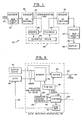
- Input data on line 22 is applied to an encoder 24 which encodes the data in the format of a limited run-length code.
- the encoder 24 may be that disclosed in the aforementioned Adler patent.
- An output signal of the encoder 24 is applied to an encoder 26 which operates in accordance with the invention for modifying the code of the encoder 24 so as to remove the average DC level.
- the modified code appears on line 28 and is coupled via a communications link 30 to a decoder 32 which operates in accordance with the invention to restore the DC level and return the format of the coded data to that appearing at the output terminal of the encoder 24.
- the output signal of the decoder 32 is applied to a further decoder 34 which provides the inverse operation of the encoder 24 so as to present the data on line 36 in the same form as the data appears on line 22.
- the data on line 36 is applied to a utilization device such as a display 38. It is noted that the data on lines 22 and 36 may be in an encoded form such as the ascii code of alpha-numeric characters, or may be a digitized version of sample analog data as would be provided by an analog-to-digital converter (not shown).
- the communication link 30 may employ a radio transmitter and receiver, or a telephone link (not shown) or as presented in the example of Figure 1, comprises a magnetic medium 40 with a recording head 42 and a playback head 44 connected thereto. Signals on line 28 are applied to the medium 40 via the recording head 42 to be stored in the medium 40. The stored data is read out of the medium 40 by means of the playback head 44, and applied by the playback head 44 to the input terminal of the decoder 32.
- the role played by the invention is found in the use of the encoder 26 and the decoder 32.
- the encoder 26 modifies an incoming digitized signal, such as that exemplified by the aforementioned code of the Adler patent, so as to remove the DC level and thereby prepare the digitized signal for further communication and by a capacitive coupling (not shown) or by the magnetic media 40.
- the decoder 32 Upon retrieval of the digitized signal from the magnetic medium 40, the decoder 32 restores the digitized signal to its previous form, such as the code of the Adler patent, so that, the digitized signal can then be utilized for its intended purpose, such as for the presentation of information on the display 38.
- the removal of the DC level is based on an examination of a present block of the code and one or more preceding blocks of the code to determine their respective contributions to a build-up of charge.
- charge herein is the same usage set forth in the foregoing patent of Patel wherein the term is used to describe both the charging which would be experienced by a capacitor through which the code is transmitted, as well as an analogous increase of voltage or current which would be experienced by an integrator through which the coded waveform passes.
- Figure 2 shows a block diagram of the encoder 26 coupled to the output terminal of the encoder 24 via a line 46 and providing the DC-free code on line 28.
- a stylized portrayal of a code signal propagating along line 46 is shown at 48.
- the encoder 26 comprises an up-down counter 50, a toggle flip-flop 52 responsive to positive and negative transitions in the waveform of the code signal 48 and providing an output signal on line 54, a clock 56, a counter 58, an accumulator 60, a frequency scaler 62, a buffer store 64, a code modifier 66, and a logic unit 68 with two sign detectors 70 and 72 coupled to input terminals thereof.
- the counter 50 serves as an integrator which counts clock pulses from the clock 56.
- the output signal of the flip-flop 52 changes state with each transition in the waveform of the code signal 48, and is applied via line 54 to an up/down control terminal of the counter 50.
- the counter 50 counts up in response to a signal on line 54 indicating a relatively high voltage portion of the signal 48, as sensed by the flip-flop 52.
- the counter 50 counts down in response a signal on line 54 indicating a relatively low voltage portion of the signal 48, as sensed by the flip-flop 52.
- pulses of the clock 56 are employed also for driving the encoder 24.
- the counter 58 counts pulses of the clock 56 so as to provide a count representative of the length of a code word of the signal 48.
- the counter 58 is set to provide an output signal on line 74 upon the conclusion of each block of the signal 48.
- each block of the code has 30 bits, and, accordingly, the counter 58 would be set to a value of 30 for use with the foregoing Adler code.
- the counter 58 Upon reaching the count of 30, the counter 58 generates the pulse on line 74 which resets the counter 58, and also resets the counter 50 and strobes the accumulator 60.
- the total count of the counter 50 is representative of the charge accumulated by the block of the code.
- the charge may have a zero value, or a non-zero value which is either positive or negative.
- the count of the counter 50 is stored in the accumulator 60 upon the strobing thereof by the signal on line 74. Thereby, the accumulator 60 stores a history of past buildup of charge, while the output of the counter 50 is the value of the charge of the most recent block.
- the output count of the counter 50 is applied to the detector 70 which detects whether the count, or charge represented by the count, is positive or negative.
- the positive or negative sign of the charge is applied by the detector 70 as an input to the logic unit 68.
- the output count, or charge, of the accumulator 60 is applied to the detector 72 which detects whether the accumulated charge is positive or negative.
- the sign of the accumulated charge is applied by the detector 72 as an input to the logic unit 68.
- the buffer store 64 receives the signal on line 46 from the encoder 24.
- the coded signal on line 46 is clocked into the store 64 by clock pulses of the clock 56.
- the bits of the coded signal are subsequently read out of the store 64 at a higher clocking rate by clock pulses applied by the frequency scaler 62.
- the scaler 62 is driven by pulses of the clock 56, and include well known counting circuitry and, possibly, an additional clock (not shown) synchronized by pulses of the counters of the scaler 62. If desired, circuitry of the scaler 62 and the clock 56 may be combined into a single clock circuit (not shown) providing output clock pulses at both a lower and a higher clock frequency.
- the buffer store 64 provides two functions, namely, the storage of the incoming coded signal on line 46 until such time as charge data of the present code word is made available by the counter 50 and an increasing of the clocking rate so as to accomodate the additional bits which are to be inserted by the code modifier 66.
- This may be explained with reference to the timing diagrams of Figure 3 wherein the upper diagram shows blocks of 30-bit code words propagating on the line 46, while the lower graph shows the corresponding 32-bit blocks appearing at the output of the code modifier 66 on line 28.
- the time duration of the 30-bit block is the same as the time duration of the 32-bit block.
- the clocking rate must be increased by the ratio of the bits (32/30).
- the logic unit 68 directs the modifier 66 either to alter the sense (positive or negative) of the charge buildup of a code block, or to leave the sense in its present state. If the signs detected by the detectors 70 and 72 are of opposite sense, this resulting in a correction of charge buildup and reduction in the DC component, the logic unit 68 commands the modifier 66 to retain the state of the charge of the present code block. In the event that the detectors 70 and 72 detect equal signs in the charges of the counter 50 and the accumulator 60, this indicating a continuing buildup of charge and of the DC component, the logic unit 68 commands the modifier 66 to invert the sense of the charge of the present code block. Thereby, the charge of the code block exiting the modifier 66 is always of the proper sense to correct the accumulation of charge.
- the code modifier 66 comprises a memory 76 which may be a read-only memory, a timing unit 78 and a gating unit 80.
- the code stored in the buffer store 64 is applied to the gating unit 80, and is also applied along with an output signal of the logic unit 68 as an address to the memory 76.
- the timing unit 78 is driven by the high clock pulses of the scaler 62 ( Figure 2), and provides timing signals for operation of the memory 76 and the gating unit 80.
- leading and trailing end portions each of which comprise six bits, are employed in the addressing of the memory 76.
- the timing unit 78 operates the memory 76 to be responsive to the occurrance of the bits in the leading and trailing end portions.
- the timing unit 78 operates the gating unit to receive all of the bits of a code block from the store 64 except for the bits of the leading and trailing end portions of the code word, and to substitute in their stead the modified set of bits for the end portions plus the additional two bits which are inserted between the code blocks.
- the modifier 66 may be constructed in the form of a programmable logic array.
- the programmable logic array (not shown) the bits of an incoming code block would be applied to a set of input lines of the array, and the bits of the output modified code block would appear on a set of output lines of the array. Interconnections between the input and output set are provided so as to perform the same function as that performed by the memory 76 and the gating unit 80 in response to the addressing provided by the signals of the store 64 and the logic unit 68.
- each code block is composed of 30 bits, and wherein two bits are inserted by the circuitry of the invention between successive ones of the code blocks.
- the rate of data propagation of the code, prior to the insertion of the additional two bits is 2/3 because the thirty bits in a code block contain only twenty bits of data.
- the error propagation of the decoder is limited; one error in the encoded bits can result in no more than ten errors in the decoded bits.
- the modification of the end portions of the code blocks results in a change in the total charge which would be accumulated. Such change would not be accounted for by the count of the counter 50, which count is based on the incoming code block, prior to modification. Accordingly, it is desirable to provide still further basis for decision of the logic unit 68, which further basis is applied via line 82 from the modifier 66.
- the memory 76 outputs projected end portions of the code blocks for both of the cases, namely inversion or noninversion of the direction of charge accumulation.
- the projected end portions are coupled via line 84 to a computer 86 of the charge increment which provides two values of charge increment, one corresponding to the case of inversion, and the other corresponding to the case of noninversion of the direction of charge accumulation.
- the modifier 66 further comprises an averaging unit 88 and a sign detector 90.
- the two possible values of charge increment are coupled via lines 92 and 94 to the averaging unit 88 which provides the average value of the two charge increments.
- the detector 90 detects the sign of the average value, and applies the average value along line 82 to the logic unit 68 for a final determination as to whether inversion or noninversion of the direction of charge accumulation is to be ordered by the address lines to the memory 76. The significance of this later step in the process will become apparent from the following mathematical description.
- the encoder inserts two bits ( y l , Y 2 ) between successive blocks of 30 bits ( ⁇ 1 ,..., 1130 ) of output from the (1,7) encoder. It may also change the values of the four bits on each end of this 30-bit block.
- W e denote the new values of the 30-bit block by ⁇ 1 ,..., 30.
- n -5 ... n 0 and ⁇ -5 ... ⁇ 0 refer to the last digits of the previous block.
- n 1 ... n 6 there are two choices for ⁇ -5 ... ⁇ 0 . ⁇ 1 ⁇ 2 . ⁇ 1 ... ⁇ 6 .
- the change in parity coincides with the change in direction of charge accumulation.
- Choice "1” has the effect of changing the direction of charge accumulation, while choice “0” leaves the direction unchanged, i.e. as it would have been in the absence of the present encoding.
- choice 0 yields the string ⁇ 0 -5 ... ⁇ 0 0 . ⁇ 0 1 ⁇ 0 2 , ⁇ 0 1 ... ⁇ 0 6
- choice 1 yields the string ⁇ 1 -5 ... a l o . ⁇ 1 1 ⁇ 1 2 . ⁇ 1 1 ... a 1 6 .
- e 0 denote the charge of the sequence ⁇ 0 -3 ... ⁇ 0 0 . ⁇ 0 1 ⁇ 0 2 . ⁇ 0 1 ... ⁇ 0 4 ' where the superscripted 0 is an index (not an exponent).
- e l denote the charge of the sequence ⁇ 1 -3 ... ⁇ 1 0 . ⁇ 1 1 ⁇ 1 2 . ⁇ 1 1 ... ⁇ 1 4 , where the superscripted 1 is an index (not an exponent).
- a parenthesized argument "(n)" indicates the location at which the function is computed, so that e 0 (n) is computed at the boundary between blocks n and n+1.
- c(n) denote the cumulative charge at four bits before the end of the nth block.
- r(n) denote the direction of charge accumulation (either +1 or -1) at that same time.
- m(n) denote the charge of the sequence n 5 ... n 26 , in block n.
- t denote the parity of the sequence ⁇ 5 ... ⁇ 26 .
- d(n) c(n) + r(n)E(n).
- d(n) will be the average of two possible values of the cumulative charge after four bits into block n+1, corresponding to the choice between blocks n and n+1.
- A(n) r (n-1) F(n-1) + r(n-1)s(n-1)m(n) + r(n-1) s(n-1)t(n)E(n).
- d(n) d(n-1) - r(n-1)F(n-1)- r(n-1)s(n-1)m(n)- r(n-1)s(n-1) t(n)E(n).
- -r(n-1)F(n-1) - r(n-1) (e 0 (n-1)-e 1 (n-1))/2.
- ⁇ (n) is bounded; its absolute value cannot exceed 19.
- d(n) is also bounded; its absolute value cannot exceed 19. Such must be the case because otherwise, the first time that
- the actual cumulative charge at any time is "close” to the value of d(n) at the nearest block boundary, and so is in turn bounded by 30.
- the following tabulation shows the interfacing bits between two contiguous code blocks (the trailing end of one block and the leading end of the succeeding block) in the left column, with substitutions therefor being shown in the middle and the right columns.
- Each substitution includes the two additional bits between the blocks, and may also provide for a change in some of the bits in the leading and the trailing ends.
- the middle column parity change
- the right column no parity change
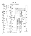
- the decoder 32 recovers the original RLL (run-length limited code) constrained bits from the RLL and charge constrained bits output by the previous encoder. It takes a block of thirty-two bits, composed of thirty data bits and two charge bits and converts it into thirty RLL constrained data bits
- the changes in the beginning and ending four bits may depend on the last (first) six bits of the preceding (succeeding) block as well as the first (last) six bits of the block itself.
- the picture is: determines
- the process described by the foregoing mathematical equations is implemented by the decoder 32 as shown in Figure 5.
- the code free of the DC level, is applied from the communication link 30 ( Figure 1) to an input register 96 of the decoder 32.
- the decoder further comprises an output register 98, a set of ten AND gates 100, 102, 104,...118, and two OR gates 120 and 122 which are connected between the registers 96 and 98.
- Input signals to the AND gates are provided by the input register 96.
- Three input signals are provided to each of the OR gates, two of the three input signals being coupled from AND gates and the third input signal being provided by the register 96.
- the connection of the signals between the register 96 and the gate follows that shown in the foregoing equations.
- the last equation is implemented by the AND gates 110 and 112, and the OR gate 122.
- Error propagation is limited.
- One error in the R L L and charge constrained bits can result in no more than eight errors in the RLL constrained bits.
- the decoder set for the foregoing Adler code (1,7) has an error propagation of six bits. When the bits are decoded to the user by first passing through the decoder 32 and 34, the error propagation is again limited.
- One error in the RLL and charge constrained bits can result in no more than ten errors in the unconstrained user bits.
- the decision process in determining whether or not an inversion is to be made can be accomplished in a further fashion as is shown with reference to Figures 2 and 4.
- the counter 50 may be coupled via a line 124 to the averaging unit 88 of the modifier 66.
- the averaging unit 88 would then sum the count of the counter 50 with each of the signals on the lines 92 and 94 to provide the complete charge accumulation which would occur over the duration of a complete block of the code, including both possible modifications of the end portions of the code block.
- the circuitry of the averaging unit 98 would be modified so that, in lieu of applying the average of the two signals to the detector 90, the averaging unit 88 would apply only the larger (in absolute value) of the two signals to the detector 90.
- the detector 90 would then be connected in lieu of the detector 70 to provide the sign of the maximum possible charge accumulation obtainable by the present code block after modification by the modifier 66.
- circuitry and coding process has provided a convenient transformation of a run-length limited code which removes the average value of the DC level so as to permit the coded signal to be transmitted via a communication link which does not respond to a DC component, and also to permit the coded signal to be stored in magnetic media. While the foregoing description has been directed to such code having a limitation (1,7), it is to be understood that the teachings of the invention are applicable to codes having other restrictions on the number of logic 0's which may be placed between logic Its.
Landscapes
- Engineering & Computer Science (AREA)
- Theoretical Computer Science (AREA)
- Compression, Expansion, Code Conversion, And Decoders (AREA)
- Signal Processing For Digital Recording And Reproducing (AREA)
- Dc Digital Transmission (AREA)
Applications Claiming Priority (2)
| Application Number | Priority Date | Filing Date | Title |
|---|---|---|---|
| US725954 | 1985-04-22 | ||
| US06/725,954 US4675650A (en) | 1985-04-22 | 1985-04-22 | Run-length limited code without DC level |
Publications (3)
| Publication Number | Publication Date |
|---|---|
| EP0199088A2 true EP0199088A2 (de) | 1986-10-29 |
| EP0199088A3 EP0199088A3 (en) | 1990-03-07 |
| EP0199088B1 EP0199088B1 (de) | 1992-12-16 |
Family
ID=24916609
Family Applications (1)
| Application Number | Title | Priority Date | Filing Date |
|---|---|---|---|
| EP86103742A Expired EP0199088B1 (de) | 1985-04-22 | 1986-03-19 | Verfahren und Anordnung zur Modifizierung eines lauflängenbegrenzten Codes |
Country Status (5)
| Country | Link |
|---|---|
| US (1) | US4675650A (de) |
| EP (1) | EP0199088B1 (de) |
| JP (1) | JPS61245720A (de) |
| CA (1) | CA1285650C (de) |
| DE (1) | DE3687285T2 (de) |
Cited By (3)
| Publication number | Priority date | Publication date | Assignee | Title |
|---|---|---|---|---|
| EP0355999A2 (de) * | 1988-07-22 | 1990-02-28 | Matsushita Electric Industrial Co., Ltd. | Kodierungs/Dekodierungssystem für optische Aufzeichnung/Wiedergabe |
| EP0503863A2 (de) * | 1991-03-15 | 1992-09-16 | International Business Machines Corporation | Lexikographisches Kodieren und Dekodieren von Zustandsabhängigen Kodes |
| EP0885978A1 (de) * | 1996-12-06 | 1998-12-23 | Kawasaki Steel Corporation | Stahlblech für doppeltgewundenes rohr und verfahren zu dessen herstellung |
Families Citing this family (22)
| Publication number | Priority date | Publication date | Assignee | Title |
|---|---|---|---|---|
| US5060242A (en) * | 1989-02-24 | 1991-10-22 | General Electric Company | Non-destructive lossless image coder |
| US5144304A (en) * | 1989-07-17 | 1992-09-01 | Digital Equipment Corporation | Data and forward error control coding techniques for digital signals |
| US5151699A (en) * | 1990-09-05 | 1992-09-29 | Pioneer Electronic Corporation | Data converting apparatus |
| JPH04185119A (ja) * | 1990-11-20 | 1992-07-02 | Matsushita Electric Ind Co Ltd | 可変長符号化装置 |
| US5625644A (en) * | 1991-12-20 | 1997-04-29 | Myers; David J. | DC balanced 4B/8B binary block code for digital data communications |
| SG85049A1 (en) * | 1992-02-19 | 2001-12-19 | Mitsubishi Electric Corp | Data conversion method and recording/reproducing apparatus using the same |
| US5550683A (en) * | 1992-12-11 | 1996-08-27 | Eastman Kodak Company | Magnetic recording channel employing a non-ideal d.c.-free equalizer and a d.c.-free modulation code |
| US5341134A (en) * | 1992-12-30 | 1994-08-23 | Datatape Incorporated | Simple coding scheme for DC free channel codes of form M/N, where M=N-1 and M and N are positive integers |
| US5424881A (en) | 1993-02-01 | 1995-06-13 | Cirrus Logic, Inc. | Synchronous read channel |
| JPH0729307A (ja) * | 1993-07-06 | 1995-01-31 | Eastman Kodak Co | データを制御極性方式で記録および検索するためのシステム |
| KR0135793B1 (ko) * | 1994-11-29 | 1998-05-15 | 김광호 | (4,20)런렝쓰 리미티드 코드 생성방법 및 장치 |
| JP3243140B2 (ja) * | 1995-02-20 | 2002-01-07 | パイオニア株式会社 | データ変換方式 |
| US6195764B1 (en) | 1997-01-30 | 2001-02-27 | Fujitsu Network Communications, Inc. | Data encoder/decoder for a high speed serial link |
| EP0944039B1 (de) * | 1997-10-07 | 2008-10-29 | Sony Corporation | Magnetaufzeichnungs - /wiedergabevorrichtung |
| US6195025B1 (en) * | 1998-07-13 | 2001-02-27 | International Business Machines Corporation | Method and means for invertibly mapping binary sequences into rate 2/3 (1,K) run-length-limited coded sequences with maximum transition density constraints |
| US7286065B1 (en) | 2001-03-05 | 2007-10-23 | Marvell International Ltd. | Method and apparatus for DC-level constrained coding |
| US6661356B1 (en) | 2001-03-05 | 2003-12-09 | Marvell International, Ltd. | Method and apparatus for DC-level constrained coding |
| KR100669623B1 (ko) * | 2001-03-12 | 2007-01-15 | 엘지전자 주식회사 | 디지털 데이터 변환방법 |
| US7084789B2 (en) * | 2003-11-17 | 2006-08-01 | Seagate Technology Llc | DC-free code having limited error propagation and limited complexity |
| US7002492B2 (en) * | 2004-07-07 | 2006-02-21 | Seagate Technology Llc | High rate running digital sum-restricted code |
| US8139628B1 (en) | 2005-01-10 | 2012-03-20 | Marvell International Ltd. | Method and device to compensate for baseline wander |
| KR20080096745A (ko) * | 2006-01-23 | 2008-11-03 | 로무 가부시키가이샤 | 부호화 장치, 복호 장치, 진폭 조정 장치, 기록 정보 판독장치, 신호 처리 장치 및 기억 시스템 |
Citations (4)
| Publication number | Priority date | Publication date | Assignee | Title |
|---|---|---|---|---|
| FR2486740A1 (fr) * | 1980-07-14 | 1982-01-15 | Philips Nv | Procede pour le codage d'une serie de blocs de bits de donnees binaires sous la forme d'une serie de blocs de bits de canal binaire et dispositif pour le decodage des bits de donnees codes selon le procede et porteur d'enregistrement pourvu d'une structure d'information |
| GB2111805A (en) * | 1981-10-29 | 1983-07-06 | Pioneer Electronic Corp | Method for converting a binary data train |
| EP0178813A2 (de) * | 1984-10-01 | 1986-04-23 | Matsushita Electric Industrial Co., Ltd. | Verfahren und Vorrichtung zur numerischen Datenkodierung |
| US4833471A (en) * | 1984-03-26 | 1989-05-23 | Canon Kabushiki Kaisha | Data processing apparatus |
Family Cites Families (6)
| Publication number | Priority date | Publication date | Assignee | Title |
|---|---|---|---|---|
| JPS5356917A (en) * | 1976-11-02 | 1978-05-23 | Olympus Optical Co Ltd | Coding system |
| JPS5619506A (en) * | 1979-07-23 | 1981-02-24 | Sony Corp | Code converting method |
| JPS5632851A (en) * | 1979-08-24 | 1981-04-02 | Matsushita Electric Ind Co Ltd | Coding and decoding system for binary information |
| JPS57132461A (en) * | 1981-02-09 | 1982-08-16 | Sony Corp | Converter for binary data code |
| US4547890A (en) * | 1982-09-28 | 1985-10-15 | Abraham M. Gindi | Apparatus and method for forming d.c. free codes |
| JPS59112409A (ja) * | 1982-12-17 | 1984-06-28 | Hitachi Denshi Ltd | 符号方式 |
-
1985
- 1985-04-22 US US06/725,954 patent/US4675650A/en not_active Expired - Fee Related
- 1985-09-18 CA CA000490980A patent/CA1285650C/en not_active Expired - Fee Related
-
1986
- 1986-03-18 JP JP61058467A patent/JPS61245720A/ja active Pending
- 1986-03-19 DE DE8686103742T patent/DE3687285T2/de not_active Expired - Fee Related
- 1986-03-19 EP EP86103742A patent/EP0199088B1/de not_active Expired
Patent Citations (4)
| Publication number | Priority date | Publication date | Assignee | Title |
|---|---|---|---|---|
| FR2486740A1 (fr) * | 1980-07-14 | 1982-01-15 | Philips Nv | Procede pour le codage d'une serie de blocs de bits de donnees binaires sous la forme d'une serie de blocs de bits de canal binaire et dispositif pour le decodage des bits de donnees codes selon le procede et porteur d'enregistrement pourvu d'une structure d'information |
| GB2111805A (en) * | 1981-10-29 | 1983-07-06 | Pioneer Electronic Corp | Method for converting a binary data train |
| US4833471A (en) * | 1984-03-26 | 1989-05-23 | Canon Kabushiki Kaisha | Data processing apparatus |
| EP0178813A2 (de) * | 1984-10-01 | 1986-04-23 | Matsushita Electric Industrial Co., Ltd. | Verfahren und Vorrichtung zur numerischen Datenkodierung |
Non-Patent Citations (2)
| Title |
|---|
| IBM TECHNICAL DISCLOSURE BULLETIN, vol. 19, no. 7, December 1976, pages 2715-2717, New York, US; A.M. PATEL: "Charge-constrained byte-oriented (0,3) code * |
| PHILIPS TECHNICAL REVIEW, vol. 40, no. 6, 1982, pages 157-165, Eindhoven, NL; J.P.J. HEEMSKERK et al.: "Compact disc: system aspects and modulation" * |
Cited By (6)
| Publication number | Priority date | Publication date | Assignee | Title |
|---|---|---|---|---|
| EP0355999A2 (de) * | 1988-07-22 | 1990-02-28 | Matsushita Electric Industrial Co., Ltd. | Kodierungs/Dekodierungssystem für optische Aufzeichnung/Wiedergabe |
| EP0355999A3 (de) * | 1988-07-22 | 1992-01-22 | Matsushita Electric Industrial Co., Ltd. | Kodierungs/Dekodierungssystem für optische Aufzeichnung/Wiedergabe |
| EP0503863A2 (de) * | 1991-03-15 | 1992-09-16 | International Business Machines Corporation | Lexikographisches Kodieren und Dekodieren von Zustandsabhängigen Kodes |
| EP0503863A3 (en) * | 1991-03-15 | 1995-07-12 | Ibm | Lexicographical encoding and decoding of state-dependent codes |
| EP0885978A1 (de) * | 1996-12-06 | 1998-12-23 | Kawasaki Steel Corporation | Stahlblech für doppeltgewundenes rohr und verfahren zu dessen herstellung |
| EP0885978A4 (de) * | 1996-12-06 | 2000-02-09 | Kawasaki Steel Co | Stahlblech für doppeltgewundenes rohr und verfahren zu dessen herstellung |
Also Published As
| Publication number | Publication date |
|---|---|
| EP0199088B1 (de) | 1992-12-16 |
| US4675650A (en) | 1987-06-23 |
| JPS61245720A (ja) | 1986-11-01 |
| DE3687285D1 (de) | 1993-01-28 |
| CA1285650C (en) | 1991-07-02 |
| EP0199088A3 (en) | 1990-03-07 |
| DE3687285T2 (de) | 1993-07-01 |
Similar Documents
| Publication | Publication Date | Title |
|---|---|---|
| EP0199088B1 (de) | Verfahren und Anordnung zur Modifizierung eines lauflängenbegrenzten Codes | |
| US4216460A (en) | Transmission and/or recording of digital signals | |
| JP3258669B2 (ja) | 改善した誤り伝搬によるトレリス・コード | |
| US4353130A (en) | Device for processing serial information which includes synchronization words | |
| US3810111A (en) | Data coding with stable base line for recording and transmitting binary data | |
| EP0415853B1 (de) | Digitales Datenübertragungssystem mit Fehlererkennung und Fehlerkorrektur | |
| EP0193153A2 (de) | Digitales Datenaufzeichnungs- und -wiedergabeverfahren | |
| PL319407A1 (en) | Method of converting a number of m-bit information words into modulated signal, method of making a record carrier medium, encoding device, decoding device, recording device, reading out device, signal as well as record carrier medium | |
| EP1056209B1 (de) | Vier-zu-sechs Kodierungstabelle, Modulation die diese anwendet, aber ohne Vereinigungsbit ,sowie ihre Anwendung für optische Plattenaufzeichnungs- oder Wiedergabesysteme | |
| GB1578635A (en) | Dc free encoding for data transmission system | |
| US3945002A (en) | Block digital processor for use with nonuniformly encoded digital words | |
| EP0577401A2 (de) | Detektion eines Synchronisationssignals und Datendemodulation | |
| KR100573626B1 (ko) | 엠비트정보워드의시퀀스를변조신호로변환하는장치및방법 | |
| EP0059224B1 (de) | Binäres datenkodier- und -dekodiersystem | |
| US4617553A (en) | Enhanced Miller code | |
| US5625505A (en) | Method of and apparatus for regenerating partial-response record signal | |
| US5175545A (en) | Data coding system in a magnetic recording apparatus | |
| GB1599155A (en) | Transmission and/or recording of digital signals | |
| EP0702827B1 (de) | Verfahren zur umwandlung von m-bit informationsworten in ein moduliertes signal, verfahren zum herstellen eines aufzeichnungsträgers, kodiervorrichtung, dekodiervorrichtung, aufzeichnungsvorrichtung, lesevorrichtung, sowie ein aufzeichnungsträger | |
| JPH05235920A (ja) | 同期化方法及びこの方法を実施する回路配置 | |
| GB2032228A (en) | DC free encoding for data transmission | |
| EP0234070B1 (de) | Vorrichtung zur binären Festlängen-Kodierung und Dekodierung | |
| US7843366B2 (en) | DVD EFM modulation architecture using two passes to reduce circuit size | |
| RU1795446C (ru) | Многоканальное устройство дл сравнени кодов | |
| JP3018980B2 (ja) | 記録符号変換装置 |
Legal Events
| Date | Code | Title | Description |
|---|---|---|---|
| PUAI | Public reference made under article 153(3) epc to a published international application that has entered the european phase |
Free format text: ORIGINAL CODE: 0009012 |
|
| AK | Designated contracting states |
Kind code of ref document: A2 Designated state(s): DE FR GB |
|
| 17P | Request for examination filed |
Effective date: 19870224 |
|
| PUAL | Search report despatched |
Free format text: ORIGINAL CODE: 0009013 |
|
| AK | Designated contracting states |
Kind code of ref document: A3 Designated state(s): DE FR GB |
|
| 17Q | First examination report despatched |
Effective date: 19901220 |
|
| GRAA | (expected) grant |
Free format text: ORIGINAL CODE: 0009210 |
|
| AK | Designated contracting states |
Kind code of ref document: B1 Designated state(s): DE FR GB |
|
| REF | Corresponds to: |
Ref document number: 3687285 Country of ref document: DE Date of ref document: 19930128 |
|
| PGFP | Annual fee paid to national office [announced via postgrant information from national office to epo] |
Ref country code: GB Payment date: 19930216 Year of fee payment: 8 |
|
| PGFP | Annual fee paid to national office [announced via postgrant information from national office to epo] |
Ref country code: FR Payment date: 19930226 Year of fee payment: 8 |
|
| ET | Fr: translation filed | ||
| PGFP | Annual fee paid to national office [announced via postgrant information from national office to epo] |
Ref country code: DE Payment date: 19930406 Year of fee payment: 8 |
|
| PLBE | No opposition filed within time limit |
Free format text: ORIGINAL CODE: 0009261 |
|
| STAA | Information on the status of an ep patent application or granted ep patent |
Free format text: STATUS: NO OPPOSITION FILED WITHIN TIME LIMIT |
|
| 26N | No opposition filed | ||
| PG25 | Lapsed in a contracting state [announced via postgrant information from national office to epo] |
Ref country code: GB Effective date: 19940319 |
|
| GBPC | Gb: european patent ceased through non-payment of renewal fee |
Effective date: 19940319 |
|
| PG25 | Lapsed in a contracting state [announced via postgrant information from national office to epo] |
Ref country code: FR Effective date: 19941130 |
|
| PG25 | Lapsed in a contracting state [announced via postgrant information from national office to epo] |
Ref country code: DE Effective date: 19941201 |
|
| REG | Reference to a national code |
Ref country code: FR Ref legal event code: ST |