EP0198429A2 - Mémoire à longueur de mot sélectionnée - Google Patents
Mémoire à longueur de mot sélectionnée Download PDFInfo
- Publication number
- EP0198429A2 EP0198429A2 EP86104924A EP86104924A EP0198429A2 EP 0198429 A2 EP0198429 A2 EP 0198429A2 EP 86104924 A EP86104924 A EP 86104924A EP 86104924 A EP86104924 A EP 86104924A EP 0198429 A2 EP0198429 A2 EP 0198429A2
- Authority
- EP
- European Patent Office
- Prior art keywords
- output
- memory
- mode
- external terminal
- transfer gate
- Prior art date
- Legal status (The legal status is an assumption and is not a legal conclusion. Google has not performed a legal analysis and makes no representation as to the accuracy of the status listed.)
- Granted
Links
Images


Classifications
-
- G—PHYSICS
- G11—INFORMATION STORAGE
- G11C—STATIC STORES
- G11C7/00—Arrangements for writing information into, or reading information out from, a digital store
- G11C7/10—Input/output [I/O] data interface arrangements, e.g. I/O data control circuits, I/O data buffers
- G11C7/1006—Data managing, e.g. manipulating data before writing or reading out, data bus switches or control circuits therefor
Definitions
- the present invention relates to an integrated circuit memory which can be used as a read only memory, a random access memory, and the like, and more specifically to such a memory whose word length can be selected in accordance with selection of a code mask.
- a integrated circuit memory such as a read only memory (ROM), a random access memory (RAM) and the like is forced to shift from N words of 8 bits to N words of 16 bits and further to N words of 32 bits.
- ROM read only memory
- RAM random access memory
- all the types of memory structures are still much in commercial demand.
- makers have to prepare all the types of memory structures. For the purpose, the makers must design a memory for each required memory structure. Otherwise, it is necessary to prepare a memory adapted such that the memory structure can be modified from external terminals.
- the former method needs a large steps of design processes and a variety of memories must be inevitably prepared, so that the efficiency of production will be low and at the same time the memories are expensive.
- the latter method is not practical since the number of the terminals is limited.
- Another object of the present invention is to provide a memory whose memory structure can be modified in the course of manufacturing process with no additional terminal.
- Still another object of the present invention is to provide a memory whose word length can be changed by only selection of a code mask used in the course of memory producing process, so that a variety of memories can be inexpensively produced at a high productivity without requiring many steps of design process.
- a memory comprising a memory cell matrix having a plurality of groups of output lines each group including at least two output lines; a plurality of groups of external terminals each group including at least two external terminals; output selection means connected between the output lines and the external terminals and adapted to connect the output lines to the corresponding external terminals in a first mode and to alternatively connect output lines of each output line group to one predetermined external terminal of the corresponding external terminal group in a second mode; control means connected to at least one given external terminal which is disconnected from the corresponding output line when the output selecting means is in the second mode, the control means being in response to a signal from the given external terminal to control the output selection means so as to cause it to selectively connect one output line of each output line group to the above predetermined external terminal of the corresponding external terminal group; and mode selection means associated to the output selection means and having a circuit structure fixed by a selected code mask so as to put the output selection means in a predetermined one of the first
- the output selection means is put either in the first mode or in the second mode by the mode selection means. If each group of output lines has two output lines, all the external terminals are active in the first mode, and therefore, the memory will have the word length equal to the number of the external terminals. In this case, the number of the words is determined by the number of the memory cells associated with each output line. In the case that the output selection means is in the second mode, one half of the external terminals are active but the other half of the external terminals are inactive. Therefore, the word length is a half of the number of the output lines, but the number of the words is twice the number of the memory cells associated with each output line.
- the one predetermined external terminal which is inactive as a data output is used as an additional address input.
- the two types of memory structures can be produced with only change of a code mask without increase of external terminal and without requiring two memory designs.
- various memory structures can be produced.
- the output selection means includes pass-through transfer gate means connected between the above predetermined external terminal of each external terminal group and the corresponding one output line of the corresponding output line group, cross transfer gate means connected between the above predetermined external terminal of each external terminal group and at least one remaining output line of the same output line group, and isolation transfer gate means connected between at least one remaining external terminal of each external terminal group and the corresponding output line.
- control means includes one input connected to the given external terminal and an output connected directly to one of the pass-through and cross transfer gate means and though an inverter to the other of the pass-through and cross transfer gate means.
- control means includes an OR gate connected at its one input to the given external terminal, and the mode selection means is connected at its output to the isolation transfer gate means and another input of the OR gate.
- mode selection means has an input selectively and fixedly connected to one of the ground and a supply voltage in accordance with the selected code mask.
- the memory cell matrix has (i+ 1 ) address input lines and 2i output lines divided into i groups each including two output lines.
- the memory has the memory structure of 2i + words of 2i bits.
- the output selection means is in the second mode, the given external terminal is used as an additional address input and the memory has the memory structure of 2 j_2 words of i bits.
- the memory cell matrix has (i+1) address input lines and 4i output lines divided into i groups each including four output lines
- the cross transfer gate means includes first, second and third cross transfer gates connected at their one end to the predetermined external terminal of each external terminal group. The other ends of these cross transfer gates are connected to the remaining three output lines of the corresponding output line group, respectively.
- the isolation transfer gate means has three isolation transfer gates between the remaining three output lines of each output line group and the corresponding external terminals, respectively, so that when the output selection means is in the second mode, all the isolation transfer gates are put in an OFF condition, and the pass-through transfer gate means and the first, second and third transfer gates are alternatively put in an ON condition by the control means.
- the mode selection means includes a first output connected to all the isolation transfer gates and a second output adapted to have the same logical level as that of the first output and connected to all the pass-through transfer gate means.
- the mode selection means also includes an input selectively and fixedly connected to one of the ground and a supply voltage in accordance with the selected code mask.
- control means includes a decoder having two inputs connected to two given external terminals which are disconnected from the corresponding output lines when the output selection means is in the first mode.
- This decoder also has four outputs connected to the pass-through transfer gate means and the first, second and third cross transfer gates, respectively, so as to put one of these transfer gates in the ON condition.
- the decoder is adapted to be activated by the mode selection means when the output selection means is in the second mode.
- the memory has the memory structure of 2 1 "words of 4i bits. But, if the output selection means is in the second mode, the two given external terminals are used as additional address inputs and the memory has the memory structure of 2 j+4 words of i bits.
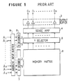
- a conventional ROM which includes a memory cell matrix 6 having a plurality of parallel outputs, which are in turn connected through a Y-selector 5, a sense amplifier 4 and an output buffer 3 to a number of output or external terminals O 0 , O 1 ... O m .
- address inputs A 0 , A 1 ... A j-1 , A j are connected to an address input buffer 9, whose outputs are connected to a X-decoder 7 and a Y-decoder 8.
- the X-decoder 7 is connected to the memory matrix 6 and the Y-decoder 8 is connected to the Y-selector.
- an address data is inputted into the address input buffer, the X-decoder 7 and the Y-decoder 8 cooperate to select memory cells to be read out.
- the data stored in the selected memory cells is read out through the Y-selector 5 and detected by the sense amplifier 4, whose outputs are further amplified by the output buffer 3 and outputted to the external terminals.
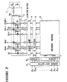
- the ROM shown in Figure 2 comprises an output selection logical circuit 2 connected between the output lines of the output buffer 3 and output or external terminals O 1 , O 2 ... O i-1 , O i , O i+1 ... O 2i-1 , O 2i /A -1 , which are divided into i pairs.
- the first pair consists of the external terminals 0, and O i+1 , the second pair of O2 and O i+2 , ... the (i-1)th pair of 0 i-1 and O 2i-1 , and the (i)-th pair of 0; and O 2i /A -1 .
- the logical circuit 2 is associated with a mode selector 1.
- the logical circuit 2 includes a pass-through transfer gates Q, connected between the first external terminal 0; - (O 1 , O 2 ... O i ) of each external terminal pair and the output of the corresponding buffer amplifier Q 5 .
- an isolation transfer gate Q3 is connected between the second external terminal Q 2i /A -1 (O i+1 , O i+2 ... O 2i-1 , O 2i /A -1 ) of each external terminal pair and the output of the corresponding buffer amplifier Q 6 .
- each first external terminal O is connected through a cross transfer gate Q2 to the connection node between the isolation transfer gate Q 3 and the corresponding buffer amplifier Q 6 .
- the second external terminal Q 2i /A -1 of the final external terminal pair is connected to one input of a NOR gate Q4, whose output CO is connected directly to a gate electrode of each cross transfer gate Q 2 and also connected through an inverter Q7 to a gate gate electrode of each pass-through gate Q 2 .
- the mode selector 1 includes a switch adapted to be connected to either the ground or a positive supply voltage Vcc in accordance with a code mask used in the course of memory production.
- An fixed terminal of the switch is connected through two cascade-connected inverters Q 8 and Q 9 to a gate electrode of each isolation transfer gate Q3 and another input of the NOR gate Q 4 .
- the output signal Bm of the inverter Q 8 is at a high level, so that the output signal CO of the NOR gate Q 4 is maintained at a low level irrespectively of the signal level of the external terminal O 2i /A -1 .
- the pass-through transfer gate Q, and the isolation transfer gate Q3 are fixed in an ON condition while the cross transfer gate Q 2 is fixed in an OFF condition. Therefore, the output signals a 2 and a 1 of the buffer amplifiers Q 5 and Q 6 are outputted to the external terminals O i and O 2i /A -1 , respectively. Namely, all the external terminals are used as data outputs, and the circuit shown in Figure 3 acts as two-bit memory output.
- the isolation transfer gate Q3 is fixed in the OFF condition, so that the external terminal O 2i /A -1 is isolated from the output a, of the buffer amplifier Q 6 .
- the output CO of the NOR gate Q 4 is determined by the logical level of the external terminal Q 2i /A -1 . Therefore, in this case, the terminal O 2i /A -1 can be used as an additional address input. If the terminal O 2i /A -1 is at a high level, the gate Q, is put in an ON condition while the gate Q 2 is put in an OFF condition.
- the output a 2 of the buffer amplifier Q 5 is outputted to the terminal Q,. If the terminal Q 2i /A -1 is at a low level, the gate Q, is OFF and the gate Qz is ON so that the output a, of the buffer amplifier Q6 is outputted to the terminal O i . Therefore, the circuit portion shown in Figure 3 functions as one-bit memory output.
- Figure 6 shows the logical conditions and the signal conditions at various points as mentioned above.
- the ROM has the address inputs A o ... A j and the output bits O, ... O 2i , i.e., the memory structure of 2 j+1 words of 2 i bits, as shown in Figure 4. In this case, all the address terminals and the external terminals are used.
- the mode selector 1 is connected to the ground by selection of another code mask, the ROM has the address inputs A -1 , A o ... A j and the output bits O 1 ... Q i , i.e., the memory structure of 2 j+2 words of i bits, as shown in Figure 5.
- the additional address input is given by the external terminal O 2i /A -1 which is one of the external terminals not used, it is not necessary to increase the terminals of the ROM.
- the above modification of the memory structure can be easily realized by selection of a code mask used in an ion implantation, a contact formation or any one of other various steps in the course of memory fabrication process. Therefore, different structures of memories can be produced in the same fabrication process just fill the fixing of the connection pattern of the mode selector. This will results in greatly increased productivity, and does not require two different memory designs for two different structurs of memories.
- FIG. 7 there is shown another embodiment of the ROM in accordance with the present invention.
- This ROM has (j+1) address inputs A o ... A (not shown) and 4i external terminals O 1 , O 2 ..., O i , ..., O 2i , ..., O 3i /A -1 , ..., O 4i /A -2 , - (only a portion is shown). Further, each four external terminals constitute one external terminal group.
- a first external terminal O; of each external terminal group is connected through a pass-through transfer gate Q, to the corresponding buffer amplifier 3.
- the remaining three external terminals O 2 ;, O 3i /A -1 and O 4i /A -2 of each group are connected to the corresponding buffer amplifiers 3 through three isolation transfer gates Q,,, Q 32 and Q 23 , respectively. Further, the external terminal O i is connected through three cross transfer gates Q 21 , Q 22 and Q 33 to the outputs of the buffer amplifiers 3 which are connected to the transfer gates Q3,, Q 32 and Q 33 .
- the mode selector 1 is connected through two cascade-connected inverters Q 8 , and Q 9 to the gate electrodes of all the isolation transfer gates Q 31 , Q 32 and Q 33 .
- the output of the inverter Q 9 is connected through an inverter 82 and an OR gate Q 41 to the gate electrode of the pass-through transfer gate Q,.
- the external terminals Q 3i /A -1 and O 4i /A -2 are connected to a decoder which includes four AND gates Q,,, Q 12 , Q 13 and Q 14 and two inverters Q, 5 and Q 16 connected as shown in Figure 7 for decoding a binary data of two bits.
- the AND gate Q is a two-input AND gate whose output is connected to another input of the OR gate Q 41 .
- the AND gates Q 12 , Q 13 and Q,4 are three-input AND gates, each of which has its one input connected to the output of the inverter Q 9 .
- the AND gates Q 12 , Q 13 and Q 14 are connected at their outputs to the gate electrodes of the cross transfer gates Q 21 , 022 and Q 23 , respectively.
- the terminal O 3i /A -1 is connected directly to the AND gates Q,, and Q 13 and also through the inverter Q 15 to the AND gates Q 12 and Q 14 .
- the terminal Q 3i /A -2 is connected to directly to the AND gates Q,, and Q,. and through the inverter Q 16 to the AND gates Q 12 and Q 13 .
- the mode selector 1 is connected to Vcc, the output signal of the inverters Q 81 and Q 82 is at a high level, so- that the output signal of the OR gate Q 41 is maintained at a low level irrespectively of the signal level of the external terminals Q 3i /A -1 and O 4i /A -2 .
- the pass-through transfer gate Q, and the isolation transfer gates Q 31 , Q 32 and Q 33 are fixed in an ON condition.
- the output of the inverter Q 9 since the output of the inverter Q 9 is low, the outputs of the AND gates Q 12 , Q, 3 and Q 14 are fixed at a low level, so that the cross transfer gates Q 21 , Q 22 and Q 23 are fixed in an OFF condition.
- the output signals of the buffer amplifiers 3 are outputted to the external terminals O i , O 2i , O 3i /A -1 and O 4i /A -1 , respectively. Namely, all the external terminals are used as data outputs. Therefore, the ROM has the address inputs A o ... A j and the output bits O i ... O 4i /A -2 , i.e., the memory structure of 2 j+1 words of 4•i bits.
- the isolation transfer gates Q 31 , Q 32 and Q 33 are fixed in the OFF condition, so that the external terminals O 2i , O 3i /A -1 and O 4i /A -2 are isolated from the outputs of the associated buffer amplifiers.
- the conditions of the transfer gates Q 1 , Q 21 , Q 22 and Q 23 are determined by the logical levels of the terminals O 3i /A -1 and O 4i /A -2 . Therefore, these external terminals are used as additional address inputs.
- the transfer gate Q With the terminals O 3i /A -1 and 0 4i /A -2 of "1, 1 ", the transfer gate Q, is ON, and Q 21 , Q 22 and Q 23 are OFF. With the combination of “0, 0", the transfer gate Q 21 is ON, and Q,, Q22 and Q n are OFF. With “1, 0”, Q 22 is ON, and Q,, Q 21 and Q,, are OFF. Further, with “0, 1 ", Q 23 is ON and Q,, Q 21 and Q 22 are OFF. Therefore, the ROM has the address inputs A. 2 , A -1 , A o ...A j and the output bits 0.... O;, i.e., the memory structure of 2 j+4 words of i bits.
Landscapes
- Read Only Memory (AREA)
- Semiconductor Memories (AREA)
Applications Claiming Priority (2)
| Application Number | Priority Date | Filing Date | Title |
|---|---|---|---|
| JP7573485 | 1985-04-10 | ||
| JP75734/85 | 1985-04-10 |
Publications (3)
| Publication Number | Publication Date |
|---|---|
| EP0198429A2 true EP0198429A2 (fr) | 1986-10-22 |
| EP0198429A3 EP0198429A3 (en) | 1988-08-17 |
| EP0198429B1 EP0198429B1 (fr) | 1991-07-24 |
Family
ID=13584796
Family Applications (1)
| Application Number | Title | Priority Date | Filing Date |
|---|---|---|---|
| EP86104924A Expired EP0198429B1 (fr) | 1985-04-10 | 1986-04-10 | Mémoire à longueur de mot sélectionnée |
Country Status (4)
| Country | Link |
|---|---|
| US (1) | US4706219A (fr) |
| EP (1) | EP0198429B1 (fr) |
| JP (1) | JPH079976B2 (fr) |
| DE (1) | DE3680371D1 (fr) |
Cited By (8)
| Publication number | Priority date | Publication date | Assignee | Title |
|---|---|---|---|---|
| EP0590953A2 (fr) * | 1992-09-29 | 1994-04-06 | Nec Corporation | Dispositif de mémoire à semi-conducteurs |
| EP0785556A3 (fr) * | 1995-12-22 | 1998-07-01 | Colwell, Robert C. | Tampons de sortie en parallèle dans des circuits de mémoire |
| EP0696801A3 (fr) * | 1994-08-12 | 1998-09-23 | Nec Corporation | Dispositif de mémoire à semi-conducteurs synchrone à basse consommation |
| EP0869617A1 (fr) * | 1997-04-04 | 1998-10-07 | Nippon Steel Semiconductor Corp. | Circuit de sélection d'entrée pour utilisation avec configuration par fil de liaison |
| WO2005022542A1 (fr) * | 2003-08-25 | 2005-03-10 | Zentrum Mikroelektronik Dresden Ag | Procede et dispositif de production de puces memoire contenant differentes largeurs de bits de donnees |
| EP1587112A2 (fr) * | 2004-01-28 | 2005-10-19 | Rambus Inc. | Module de mémoire à tampon avec largeur d'interface configurable. |
| US9865329B2 (en) | 2005-09-26 | 2018-01-09 | Rambus Inc. | Memory system topologies including a buffer device and an integrated circuit memory device |
| US11328764B2 (en) | 2005-09-26 | 2022-05-10 | Rambus Inc. | Memory system topologies including a memory die stack |
Families Citing this family (11)
| Publication number | Priority date | Publication date | Assignee | Title |
|---|---|---|---|---|
| JPH0736269B2 (ja) * | 1985-08-30 | 1995-04-19 | 株式会社日立製作所 | 半導体記憶装置 |
| US4819212A (en) * | 1986-05-31 | 1989-04-04 | Kabushiki Kaisha Toshiba | Nonvolatile semiconductor memory device with readout test circuitry |
| JPS635444A (ja) * | 1986-06-25 | 1988-01-11 | Hitachi Ltd | マイクロプロセツサ |
| US5265045A (en) * | 1986-10-31 | 1993-11-23 | Hitachi, Ltd. | Semiconductor integrated circuit device with built-in memory circuit group |
| US5257234A (en) * | 1987-07-15 | 1993-10-26 | Hitachi, Ltd. | Semiconductor integrated circuit device |
| EP0299697B1 (fr) * | 1987-07-15 | 1993-09-29 | Hitachi, Ltd. | Dispositif de circuit intégré à semi-conducteurs |
| JPH0697560B2 (ja) * | 1987-11-19 | 1994-11-30 | 三菱電機株式会社 | 半導体記憶装置 |
| JP2600304B2 (ja) * | 1988-06-30 | 1997-04-16 | 三菱電機株式会社 | 半導体記憶装置とこれを用いたデータパス |
| JPH02168496A (ja) * | 1988-09-14 | 1990-06-28 | Kawasaki Steel Corp | 半導体メモリ回路 |
| KR100532471B1 (ko) * | 2003-09-26 | 2005-12-01 | 삼성전자주식회사 | 입출력 데이터 위스 조절이 가능한 메모리 장치 및 그위스 조절 방법 |
| US7464225B2 (en) | 2005-09-26 | 2008-12-09 | Rambus Inc. | Memory module including a plurality of integrated circuit memory devices and a plurality of buffer devices in a matrix topology |
Citations (4)
| Publication number | Priority date | Publication date | Assignee | Title |
|---|---|---|---|---|
| JPS5357932A (en) * | 1976-11-05 | 1978-05-25 | Hitachi Ltd | Semiconductor memory element |
| JPS54128226A (en) * | 1978-03-29 | 1979-10-04 | Hitachi Ltd | Random access memory |
| EP0018843A1 (fr) * | 1979-05-04 | 1980-11-12 | Fujitsu Limited | Dispositif de mémoire à semi-conducteurs avec portes de sortie parallèles |
| JPS5860480A (ja) * | 1981-10-06 | 1983-04-09 | Nippon Telegr & Teleph Corp <Ntt> | 半導体メモリ |
Family Cites Families (2)
| Publication number | Priority date | Publication date | Assignee | Title |
|---|---|---|---|---|
| JPS57127989A (en) * | 1981-02-02 | 1982-08-09 | Hitachi Ltd | Mos static type ram |
| JPH0652784B2 (ja) * | 1984-12-07 | 1994-07-06 | 富士通株式会社 | ゲートアレイ集積回路装置及びその製造方法 |
-
1986
- 1986-04-10 US US06/850,302 patent/US4706219A/en not_active Expired - Lifetime
- 1986-04-10 DE DE8686104924T patent/DE3680371D1/de not_active Expired - Lifetime
- 1986-04-10 JP JP8349586A patent/JPH079976B2/ja not_active Expired - Lifetime
- 1986-04-10 EP EP86104924A patent/EP0198429B1/fr not_active Expired
Patent Citations (4)
| Publication number | Priority date | Publication date | Assignee | Title |
|---|---|---|---|---|
| JPS5357932A (en) * | 1976-11-05 | 1978-05-25 | Hitachi Ltd | Semiconductor memory element |
| JPS54128226A (en) * | 1978-03-29 | 1979-10-04 | Hitachi Ltd | Random access memory |
| EP0018843A1 (fr) * | 1979-05-04 | 1980-11-12 | Fujitsu Limited | Dispositif de mémoire à semi-conducteurs avec portes de sortie parallèles |
| JPS5860480A (ja) * | 1981-10-06 | 1983-04-09 | Nippon Telegr & Teleph Corp <Ntt> | 半導体メモリ |
Non-Patent Citations (4)
| Title |
|---|
| EDN ELECTRICAL DESIGN NEWS, vol. 23, no. 17, 20th September 1978, pages 89-93, Denver, US; C.A. OGDIN: "Reconfigurable memory scheme suits 8- or 16-bit words" * |
| PATENT ABSTRACTS OF JAPAN, vol. 2, no. 94, 5th August 1978, page 4403 E 78; & JP-A-53 57 932 (HITACHI SEISAKUSHO K.K.) 25-05-1978 * |
| PATENT ABSTRACTS OF JAPAN, vol. 3, no. 149 (E-157), 8th December 1979, page 57 E 157; & JP-A-54 128 226 (HITACHI SEISAKUSHO K.K.) 04-10-1979 * |
| PATENT ABSTRACTS OF JAPAN, vol. 7, no. 150 (P-207)[1295], 30th June 1983; & JP-A-58 60 480 (NIPPON DENSHIN DENWA KOSHA) 09-04-1983 * |
Cited By (17)
| Publication number | Priority date | Publication date | Assignee | Title |
|---|---|---|---|---|
| EP0590953A2 (fr) * | 1992-09-29 | 1994-04-06 | Nec Corporation | Dispositif de mémoire à semi-conducteurs |
| EP0590953A3 (fr) * | 1992-09-29 | 1994-08-03 | Nec Corp | |
| US5381378A (en) * | 1992-09-29 | 1995-01-10 | Nec Corporation | Semiconductor memory device |
| EP0696801A3 (fr) * | 1994-08-12 | 1998-09-23 | Nec Corporation | Dispositif de mémoire à semi-conducteurs synchrone à basse consommation |
| EP0785556A3 (fr) * | 1995-12-22 | 1998-07-01 | Colwell, Robert C. | Tampons de sortie en parallèle dans des circuits de mémoire |
| EP0869617A1 (fr) * | 1997-04-04 | 1998-10-07 | Nippon Steel Semiconductor Corp. | Circuit de sélection d'entrée pour utilisation avec configuration par fil de liaison |
| US5900021A (en) * | 1997-04-04 | 1999-05-04 | United Memories, Inc. | Pad input select circuit for use with bond options |
| WO2005022542A1 (fr) * | 2003-08-25 | 2005-03-10 | Zentrum Mikroelektronik Dresden Ag | Procede et dispositif de production de puces memoire contenant differentes largeurs de bits de donnees |
| EP1587112A2 (fr) * | 2004-01-28 | 2005-10-19 | Rambus Inc. | Module de mémoire à tampon avec largeur d'interface configurable. |
| EP1587112A3 (fr) * | 2004-01-28 | 2006-06-21 | Rambus Inc. | Module de mémoire à tampon avec largeur d'interface configurable. |
| US9865329B2 (en) | 2005-09-26 | 2018-01-09 | Rambus Inc. | Memory system topologies including a buffer device and an integrated circuit memory device |
| US10381067B2 (en) | 2005-09-26 | 2019-08-13 | Rambus Inc. | Memory system topologies including a buffer device and an integrated circuit memory device |
| US10535398B2 (en) | 2005-09-26 | 2020-01-14 | Rambus Inc. | Memory system topologies including a buffer device and an integrated circuit memory device |
| US10672458B1 (en) | 2005-09-26 | 2020-06-02 | Rambus Inc. | Memory system topologies including a buffer device and an integrated circuit memory device |
| US11043258B2 (en) | 2005-09-26 | 2021-06-22 | Rambus Inc. | Memory system topologies including a memory die stack |
| US11328764B2 (en) | 2005-09-26 | 2022-05-10 | Rambus Inc. | Memory system topologies including a memory die stack |
| US11727982B2 (en) | 2005-09-26 | 2023-08-15 | Rambus Inc. | Memory system topologies including a memory die stack |
Also Published As
| Publication number | Publication date |
|---|---|
| JPH079976B2 (ja) | 1995-02-01 |
| JPS6242444A (ja) | 1987-02-24 |
| DE3680371D1 (de) | 1991-08-29 |
| US4706219A (en) | 1987-11-10 |
| EP0198429A3 (en) | 1988-08-17 |
| EP0198429B1 (fr) | 1991-07-24 |
Similar Documents
| Publication | Publication Date | Title |
|---|---|---|
| US4706219A (en) | Word length selectable memory | |
| EP0096359B1 (fr) | Dispositif de mémoire semi-conductrice | |
| US5089992A (en) | Semiconductor memory device and a data path using the same | |
| US5590084A (en) | Semiconductor memory device having a column selector | |
| EP0361404B1 (fr) | Circuit de mémoire muni d'une structure de redondance améliorée | |
| EP0385389B1 (fr) | Circuit de mémoire à semi-conducteurs intégré pouvant masquer l'écriture de mémoire | |
| EP0408002A2 (fr) | Appareil de mémoire programmable à semi-conducteurs | |
| EP0171718B1 (fr) | Circuit décodeur dans un chip de mémoire intégrée | |
| JPH0378720B2 (fr) | ||
| US5452258A (en) | Semiconductor read only memory | |
| US4922441A (en) | Gate array device having a memory cell/interconnection region | |
| EP0213835B1 (fr) | Dispositif de mémoire semi-conductrice | |
| US4634900A (en) | Sense amplifier | |
| EP0202910B1 (fr) | Circuit décodeur pour un dispositif de mémoire semi-conducteur | |
| US5218572A (en) | Semiconductor memory device | |
| EP0055582B1 (fr) | Circuit de mémoire à décodeur | |
| US6304480B1 (en) | Read only memory integrated semiconductor device | |
| EP0264933B1 (fr) | Système avec rétrocouplage négatif pour réduire le temps de réponse d'une cellule de mémoire | |
| JP2982902B2 (ja) | 半導体メモリ | |
| GB2163616A (en) | A memory device | |
| US4719595A (en) | Data output circuit for a dynamic memory | |
| USRE38651E1 (en) | Variable depth and width memory device | |
| JP2658267B2 (ja) | 半導体メモリの冗長回路 | |
| US20010028574A1 (en) | Via code Mask ROM | |
| KR100280391B1 (ko) | 소수의 셀을 갖는 롬 구조 |
Legal Events
| Date | Code | Title | Description |
|---|---|---|---|
| PUAI | Public reference made under article 153(3) epc to a published international application that has entered the european phase |
Free format text: ORIGINAL CODE: 0009012 |
|
| 17P | Request for examination filed |
Effective date: 19860410 |
|
| AK | Designated contracting states |
Kind code of ref document: A2 Designated state(s): DE FR GB |
|
| PUAL | Search report despatched |
Free format text: ORIGINAL CODE: 0009013 |
|
| AK | Designated contracting states |
Kind code of ref document: A3 Designated state(s): DE FR GB |
|
| 17Q | First examination report despatched |
Effective date: 19890613 |
|
| GRAA | (expected) grant |
Free format text: ORIGINAL CODE: 0009210 |
|
| AK | Designated contracting states |
Kind code of ref document: B1 Designated state(s): DE FR GB |
|
| REF | Corresponds to: |
Ref document number: 3680371 Country of ref document: DE Date of ref document: 19910829 |
|
| ET | Fr: translation filed | ||
| PLBE | No opposition filed within time limit |
Free format text: ORIGINAL CODE: 0009261 |
|
| STAA | Information on the status of an ep patent application or granted ep patent |
Free format text: STATUS: NO OPPOSITION FILED WITHIN TIME LIMIT |
|
| 26N | No opposition filed | ||
| REG | Reference to a national code |
Ref country code: GB Ref legal event code: IF02 |
|
| REG | Reference to a national code |
Ref country code: GB Ref legal event code: 732E |
|
| REG | Reference to a national code |
Ref country code: FR Ref legal event code: TQ |
|
| PGFP | Annual fee paid to national office [announced via postgrant information from national office to epo] |
Ref country code: GB Payment date: 20050406 Year of fee payment: 20 |
|
| PGFP | Annual fee paid to national office [announced via postgrant information from national office to epo] |
Ref country code: DE Payment date: 20050407 Year of fee payment: 20 |
|
| PGFP | Annual fee paid to national office [announced via postgrant information from national office to epo] |
Ref country code: FR Payment date: 20050408 Year of fee payment: 20 |
|
| REG | Reference to a national code |
Ref country code: GB Ref legal event code: PE20 |
|
| PG25 | Lapsed in a contracting state [announced via postgrant information from national office to epo] |
Ref country code: GB Free format text: LAPSE BECAUSE OF EXPIRATION OF PROTECTION Effective date: 20060409 |