EP0184290B1 - Verfahren zum Herstellen von Halbleiterbauelementen unter Verwendung eines Dual-Peak-Laserstrahls - Google Patents
Verfahren zum Herstellen von Halbleiterbauelementen unter Verwendung eines Dual-Peak-Laserstrahls Download PDFInfo
- Publication number
- EP0184290B1 EP0184290B1 EP85307109A EP85307109A EP0184290B1 EP 0184290 B1 EP0184290 B1 EP 0184290B1 EP 85307109 A EP85307109 A EP 85307109A EP 85307109 A EP85307109 A EP 85307109A EP 0184290 B1 EP0184290 B1 EP 0184290B1
- Authority
- EP
- European Patent Office
- Prior art keywords
- laser beam
- polycrystalline silicon
- silicon film
- power distribution
- fresnel
- Prior art date
- Legal status (The legal status is an assumption and is not a legal conclusion. Google has not performed a legal analysis and makes no representation as to the accuracy of the status listed.)
- Expired - Lifetime
Links
Images


Classifications
-
- G—PHYSICS
- G02—OPTICS
- G02B—OPTICAL ELEMENTS, SYSTEMS OR APPARATUS
- G02B27/00—Optical systems or apparatus not provided for by any of the groups G02B1/00 - G02B26/00, G02B30/00
- G02B27/09—Beam shaping, e.g. changing the cross-sectional area, not otherwise provided for
-
- H—ELECTRICITY
- H10—SEMICONDUCTOR DEVICES; ELECTRIC SOLID-STATE DEVICES NOT OTHERWISE PROVIDED FOR
- H10P—GENERIC PROCESSES OR APPARATUS FOR THE MANUFACTURE OR TREATMENT OF DEVICES COVERED BY CLASS H10
- H10P14/00—Formation of materials, e.g. in the shape of layers or pillars
- H10P14/20—Formation of materials, e.g. in the shape of layers or pillars of semiconductor materials
- H10P14/38—Formation of materials, e.g. in the shape of layers or pillars of semiconductor materials characterised by treatments done after the formation of the materials
- H10P14/3802—Crystallisation or recrystallisation of non-monocrystalline semiconductor materials, e.g. regrowth
- H10P14/3808—Crystallisation or recrystallisation of non-monocrystalline semiconductor materials, e.g. regrowth using laser beams
-
- G—PHYSICS
- G02—OPTICS
- G02B—OPTICAL ELEMENTS, SYSTEMS OR APPARATUS
- G02B27/00—Optical systems or apparatus not provided for by any of the groups G02B1/00 - G02B26/00, G02B30/00
- G02B27/09—Beam shaping, e.g. changing the cross-sectional area, not otherwise provided for
- G02B27/0911—Anamorphotic systems
-
- G—PHYSICS
- G02—OPTICS
- G02B—OPTICAL ELEMENTS, SYSTEMS OR APPARATUS
- G02B27/00—Optical systems or apparatus not provided for by any of the groups G02B1/00 - G02B26/00, G02B30/00
- G02B27/09—Beam shaping, e.g. changing the cross-sectional area, not otherwise provided for
- G02B27/0938—Using specific optical elements
- G02B27/095—Refractive optical elements
- G02B27/0972—Prisms
-
- H—ELECTRICITY
- H10—SEMICONDUCTOR DEVICES; ELECTRIC SOLID-STATE DEVICES NOT OTHERWISE PROVIDED FOR
- H10P—GENERIC PROCESSES OR APPARATUS FOR THE MANUFACTURE OR TREATMENT OF DEVICES COVERED BY CLASS H10
- H10P14/00—Formation of materials, e.g. in the shape of layers or pillars
- H10P14/20—Formation of materials, e.g. in the shape of layers or pillars of semiconductor materials
- H10P14/29—Formation of materials, e.g. in the shape of layers or pillars of semiconductor materials characterised by the substrates
- H10P14/2901—Materials
- H10P14/2902—Materials being Group IVA materials
- H10P14/2905—Silicon, silicon germanium or germanium
-
- H—ELECTRICITY
- H10—SEMICONDUCTOR DEVICES; ELECTRIC SOLID-STATE DEVICES NOT OTHERWISE PROVIDED FOR
- H10P—GENERIC PROCESSES OR APPARATUS FOR THE MANUFACTURE OR TREATMENT OF DEVICES COVERED BY CLASS H10
- H10P14/00—Formation of materials, e.g. in the shape of layers or pillars
- H10P14/20—Formation of materials, e.g. in the shape of layers or pillars of semiconductor materials
- H10P14/32—Formation of materials, e.g. in the shape of layers or pillars of semiconductor materials characterised by intermediate layers between substrates and deposited layers
- H10P14/3202—Materials thereof
- H10P14/3238—Materials thereof being insulating materials
-
- H—ELECTRICITY
- H10—SEMICONDUCTOR DEVICES; ELECTRIC SOLID-STATE DEVICES NOT OTHERWISE PROVIDED FOR
- H10P—GENERIC PROCESSES OR APPARATUS FOR THE MANUFACTURE OR TREATMENT OF DEVICES COVERED BY CLASS H10
- H10P14/00—Formation of materials, e.g. in the shape of layers or pillars
- H10P14/20—Formation of materials, e.g. in the shape of layers or pillars of semiconductor materials
- H10P14/32—Formation of materials, e.g. in the shape of layers or pillars of semiconductor materials characterised by intermediate layers between substrates and deposited layers
- H10P14/3242—Structure
-
- H—ELECTRICITY
- H10—SEMICONDUCTOR DEVICES; ELECTRIC SOLID-STATE DEVICES NOT OTHERWISE PROVIDED FOR
- H10P—GENERIC PROCESSES OR APPARATUS FOR THE MANUFACTURE OR TREATMENT OF DEVICES COVERED BY CLASS H10
- H10P14/00—Formation of materials, e.g. in the shape of layers or pillars
- H10P14/20—Formation of materials, e.g. in the shape of layers or pillars of semiconductor materials
- H10P14/34—Deposited materials, e.g. layers
- H10P14/3402—Deposited materials, e.g. layers characterised by the chemical composition
- H10P14/3404—Deposited materials, e.g. layers characterised by the chemical composition being Group IVA materials
- H10P14/3411—Silicon, silicon germanium or germanium
-
- H—ELECTRICITY
- H10—SEMICONDUCTOR DEVICES; ELECTRIC SOLID-STATE DEVICES NOT OTHERWISE PROVIDED FOR
- H10P—GENERIC PROCESSES OR APPARATUS FOR THE MANUFACTURE OR TREATMENT OF DEVICES COVERED BY CLASS H10
- H10P14/00—Formation of materials, e.g. in the shape of layers or pillars
- H10P14/20—Formation of materials, e.g. in the shape of layers or pillars of semiconductor materials
- H10P14/34—Deposited materials, e.g. layers
- H10P14/3451—Structure
- H10P14/3452—Microstructure
- H10P14/3458—Monocrystalline
-
- H—ELECTRICITY
- H10—SEMICONDUCTOR DEVICES; ELECTRIC SOLID-STATE DEVICES NOT OTHERWISE PROVIDED FOR
- H10P—GENERIC PROCESSES OR APPARATUS FOR THE MANUFACTURE OR TREATMENT OF DEVICES COVERED BY CLASS H10
- H10P14/00—Formation of materials, e.g. in the shape of layers or pillars
- H10P14/20—Formation of materials, e.g. in the shape of layers or pillars of semiconductor materials
- H10P14/38—Formation of materials, e.g. in the shape of layers or pillars of semiconductor materials characterised by treatments done after the formation of the materials
- H10P14/3802—Crystallisation or recrystallisation of non-monocrystalline semiconductor materials, e.g. regrowth
- H10P14/3808—Crystallisation or recrystallisation of non-monocrystalline semiconductor materials, e.g. regrowth using laser beams
- H10P14/381—Beam shaping, e.g. using a mask
-
- H—ELECTRICITY
- H10—SEMICONDUCTOR DEVICES; ELECTRIC SOLID-STATE DEVICES NOT OTHERWISE PROVIDED FOR
- H10P—GENERIC PROCESSES OR APPARATUS FOR THE MANUFACTURE OR TREATMENT OF DEVICES COVERED BY CLASS H10
- H10P14/00—Formation of materials, e.g. in the shape of layers or pillars
- H10P14/20—Formation of materials, e.g. in the shape of layers or pillars of semiconductor materials
- H10P14/38—Formation of materials, e.g. in the shape of layers or pillars of semiconductor materials characterised by treatments done after the formation of the materials
- H10P14/3802—Crystallisation or recrystallisation of non-monocrystalline semiconductor materials, e.g. regrowth
- H10P14/3808—Crystallisation or recrystallisation of non-monocrystalline semiconductor materials, e.g. regrowth using laser beams
- H10P14/3814—Continuous wave laser beam
-
- H—ELECTRICITY
- H10—SEMICONDUCTOR DEVICES; ELECTRIC SOLID-STATE DEVICES NOT OTHERWISE PROVIDED FOR
- H10P—GENERIC PROCESSES OR APPARATUS FOR THE MANUFACTURE OR TREATMENT OF DEVICES COVERED BY CLASS H10
- H10P14/00—Formation of materials, e.g. in the shape of layers or pillars
- H10P14/20—Formation of materials, e.g. in the shape of layers or pillars of semiconductor materials
- H10P14/38—Formation of materials, e.g. in the shape of layers or pillars of semiconductor materials characterised by treatments done after the formation of the materials
- H10P14/3802—Crystallisation or recrystallisation of non-monocrystalline semiconductor materials, e.g. regrowth
- H10P14/382—Scanning of a beam
-
- H—ELECTRICITY
- H10—SEMICONDUCTOR DEVICES; ELECTRIC SOLID-STATE DEVICES NOT OTHERWISE PROVIDED FOR
- H10P—GENERIC PROCESSES OR APPARATUS FOR THE MANUFACTURE OR TREATMENT OF DEVICES COVERED BY CLASS H10
- H10P34/00—Irradiation with electromagnetic or particle radiation of wafers, substrates or parts of devices
- H10P34/40—Irradiation with electromagnetic or particle radiation of wafers, substrates or parts of devices with high-energy radiation
- H10P34/42—Irradiation with electromagnetic or particle radiation of wafers, substrates or parts of devices with high-energy radiation with electromagnetic radiation, e.g. laser annealing
-
- Y—GENERAL TAGGING OF NEW TECHNOLOGICAL DEVELOPMENTS; GENERAL TAGGING OF CROSS-SECTIONAL TECHNOLOGIES SPANNING OVER SEVERAL SECTIONS OF THE IPC; TECHNICAL SUBJECTS COVERED BY FORMER USPC CROSS-REFERENCE ART COLLECTIONS [XRACs] AND DIGESTS
- Y10—TECHNICAL SUBJECTS COVERED BY FORMER USPC
- Y10S—TECHNICAL SUBJECTS COVERED BY FORMER USPC CROSS-REFERENCE ART COLLECTIONS [XRACs] AND DIGESTS
- Y10S117/00—Single-crystal, oriented-crystal, and epitaxy growth processes; non-coating apparatus therefor
- Y10S117/903—Dendrite or web or cage technique
- Y10S117/904—Laser beam
Definitions
- This invention relates to a process for the production of semiconductor devices, in which a SOI (Silicon on Insulator) technique is employed with a laser beam.
- SOI Silicon on Insulator
- the laser recrystallization method comprises forming a silicon oxide film on a silicon substrate and forming an amorphous or polycrystalline silicon film on the silicon oxide film, followed by irradiating the amorphous or polycrystalline silicon film with a scanning laser beam to achieve a single crystallization of the amorphous or polycrystalline silicon film.
- the laser beam in order to melt the silicion film by the irradiation of the scanning laser beam, the laser beam should be focused into a spot with a diameter of approximately 100 pm and scanned on the whole surface of the wafer.
- the trailing edge i.e., the interface between the solid region and the molten region
- An approach for attaining such a concaved trailing edge is essential to get a single crystalline region.
- the silicon film to be recrystallized is made of a particular lamination structure to control the reflectivity and/or the thermal conductivity to the substrate, resulting in a concaved trailing edge.
- This approach is disadvantageous in that the single crystalline region must have a width of as small as approximately 20 11m since the trailing edge must be changed from convex to concave due to the particular structure of the sample film. This causes power losses.
- the Gaussian distribution of the laser beam is transformed into a dual peak type power distribution with peaks at both ends and a valley in the center portion, and then the silicon film is irradiated with the laser beam having a dual type power distribution resulting in a concaved trialing edge.
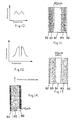
- the Gaussian beam ( Figure 7(a)) is used for the irradiation of the sample film, the film is molten and a number of grains start to grow from both ends of the molten region of a low temperature to the center portion thereof of a high temperature, resulting in aggregation of polycrystals as shown in Figure 14.
- the laser beam used for the achievement of a single recrystallization must exhibit a dual peak type power distribution rather than the Gaussian distribution.
- EP-A-0071471 uses a plurality of high energy beams which have a Gaussian distribution.
- the molten film recrystallizes from the central part toward the outer edge.
- the process for the production of semiconductor devices of this invention comprises (I) forming a first oxide film on a semiconductor substrate, (II) forming a groove or grooves on the first oxide film, (III) forming a first polycrystalline silicon film as an active layer on the whole surface of the first oxide film, (IV) forming a second oxide film on the first polycrystalline silicon film, (V) forming a second polycrystalline silicon film on the second oxide film, said second polycrystalline silicon film serving as a buffer layer which absorbs the fluctuation of a scanning laser beam irradiating the first polycrystalline silicon film in step (VII), (VI) forming an antireflection film made of an oxide film on said buffer layer, and (VII) irradiating the first polycrystalline silicon film with a scanning laser beam having a dual peak type power distribution to melt said first polycrystalline silicon film in such a manner that both peaks in the power distribution of the laser beam are positioned at both outer sides of said
- the center of the Gaussian distribution of the power distribution of a laser beam is, in a preferred embodiment, split and the resulting halves are shifted and recombined, resulting in said scanning laser beam exhibiting a dual peak type power distribution with peaks at both ends and a valley in the center.
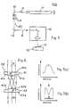
- the optical system comprises, in a preferred embodiment, in turn a laser beam source 11, a first reflecting mirror, a beam expander, a pair of Fresnel biprisms, a second reflecting mirror, scanning optics, and a heater for heating a sample disposed thereon to be subjected to a recrystallization treatment, said pair of Fresnel biprisms being positioned in such a manner that the surface containing the vertical angle of the first Fresnel biprism faces the surface containing the vertical angle of the second Fresnel biprism and the plane surface of the first Fresnel biprism is parallel to the plane surface of the second Fresnel biprism.
- the optical system comprises, in a preferred embodiment, in turn a laser beam source 11, a first reflecting mirror, a beam expander, a pair of V-shaped reflecting mirrors, a second reflecting mirror, scanning optics, and a heater for heating a sample disposed thereon to be subjected to a recrystallization treatment, said pair of V-shaped reflecting mirrors being positioned in such a manner that the reflecting surface containing the vertical angle (n-e) of the first V-shaped mirror faces and is parallel to the reflecting surface containing the vertical angle (n-e) of the second V-shaped mirror.
- the invention described herein makes possible the objects of (1) providing a recrystallization process in which single crystallization of non-single crystalline thin films such as a polycrystalline silicon film, an amorphous silicon film, etc., can be stably attained on the whole region of a wafer, using a scanning laser beam having a power distribution with peaks at both ends and a valley in the center; (2) providing a process for the production of semiconductor devices in which good quality devices can be fabricated on the single crystalline region obtained by the above-mentioned recrystallization process; (3) providing a process for the production of semiconductor devices from which three-dimensional integrated circuits can be produced; (4) providing an apparatus with a simple structure for the production of single crystalline thin films, which comprises a known laser-annealing apparatus and a pair of Fresnel biprisms onr a pair of V-shaped reflecting mirrors; and (5) providing an apparatus for the emission of laser beam with a dual peak type power distribution which allows for the formation of widely striped single-crystalline regions on
- the process for the production of semiconductor devices of this invention comprises forming a first oxide film on a semiconductor substrate; forming grooves on the area to be single-crystallized in such a manner that the bottom of each of the grooves does not penetrate the first oxide film; forming a first polycrystalline silicon film serving as an active layer on the whole surface of the first oxide film including the grooves; forming a second oxide film on the first polycrystalline silicon film serving as an active layer; forming a second polycrystalline silicon film on the second oxide film, said second polycrystalline silicon film serving as a buffer layer for absorbing the fluctuation of a scanning laser beam irradiating the first polycrystalline silicon film; forming an anti-reflection film made of an oxide film on the second polycrystalline silicon film serving as a buffer layer; irradiating the first polycrystalline silicon film with the scanning laser beam having a dual peak type power distribution to melt the first polycrystalline silicon film in such a manner that both peaks in the power distribution of the laser beam are positioned at both outer sides of the grooves, respectively, thereby
- the temperature distribution of the irradiated area exhibits a pattern in which the temperature in the center of the area to be single-crystallized is significantly lower than that of the outer sides of each of the grooves. This temperature distribution characteristic is maintained, and even though the power distribution of the laser beam varies to a certain extent, the above-mentioned temperature distribution never reverses, resulting in a high quality single crystal in the given area of the active layer.
- turbulence at the interface between the solid area and the molten area in the active layer due to the fluctuation of the laser beam is made smooth by heat diffusion on the surface of the buffer layer positioned above the active layer, so that a stable single crystal growth can be attained in the active layer.
- Figure 1 shows the sectional view of the area in a sample to be subjected to a recrystallization treatment where devices should be fabricated.
- the sample is prepared as followed: On a silicon substrate 1, a silicon oxide film 2 having a thickness of 1.5 11m is formed. Then, grooves 21 having a depth of 0.3 pm, a width of 80 ⁇ m and a space therebetween of approximately 20 11m are formed in the area of the silicon oxide film 2 to be single-crystallized.
- the length of each of the grooves 21 is not limited.
- a polycrystalline silicon film 3a serving as an active layer and a silicon oxide film 4a are successively formed with a thickness of 0.5 11m and 0.2 pm, respectively, by chemical vapor deposition.
- a polycrystalline silicon film 3b serving as a buffer layer and a silicon oxide film 4b serving as an anti-reflection film are successively formed with a thickness of 0.5 11m and 0.26 pm, respectively, by chemical vapor deposition.
- the polycrystalline silicon film 3a is the layer on which devices should be fabricated, and the other polycrystalline silicon film 3b positioned above the polycrystalline silicon film 3a functions as a buffer layer.
- the resulting sample is irradiated with a scanning argon laser beam (with a power of 7 watts and a scanning rate of 10 cm/sec), which exhibits a dual peak type power distribution, in such a manner that, as shown in Figure 2, both peaks 61 in the power distribution of the laser beam 6 are positioned at both outer sides 210 of each of the grooves 21.
- the resulting temperature distribution of the sample exhibits that, as shown in Figure 3, the temperature of the center area of each of the grooves 21 is extremely low as compared with the outer sides 210 of each of the grooves 21.
- each of the grooves 21 at the lowest temperature starts to be crystallized and crystallization stably proceeds toward both sides 210 of each of the grooves 21, resulting in a single crystalline region 8 within each of the grooves 21.
- Reference numeral 7 in Figure 3 indicates subboundaries formed on the outer sides 210 of the grooves 21.
- both polycrystalline silicion films 3a and 3b in the grooves 21 are simultaneously single-crystallized.
- a comparison of the crystalline state ( Figure 4(a)) after achieving recrystallization of the buffer layer (the upper layer) 3b with the crystalline state ( Figure 4(b)) after recrystallization of the active layer (the lower layer) 3a is as follows: Subboundaries derived from the boundaries 9 are limited to the convex area of both the upper layer 3b and the lower layer 3a and do not extend to the area of each of the grooves 21 where devices should be fabricated. However, twin boundaries 10 exist in the region from the convex area to the concave area of the upper layer 3b.
- Figure 5 shows an example of optical systems used to transform the power distribution of a laser beam from the Gaussian distribution ( Figure 7(a)) into a dual peak type distribution ( Figure 7(b)) according to this invention, which comprises a known laser annealing apparatus 100 and a pair of Fresnel biprisms 40.
- the laser annealing apparatus 100 comprises in turn a laser beam source 11, reflecting mirrors 12 and 13, a beam expander 14, scanning optics 15, and a heater 16 for heating a sample 17, which is disposed thereon to be subjected to a recrystallization treatment according to the above-mentioned processes.
- the pair of Fresnel biprisms 40 are disposed between the beam expander 14 and the reflecting mirror 13 in such a manner that, as shown in Figure 6, the surface containing the vertical angle O of the first Fresnel biprism 41 faces the surface containing the vertical angle O of the second Fresnel biprism 42 and the plane surface 41a of the first Fresnel biprism 41 is parallel to the plane surface 42a of the second Fresnel biprism.
- the center of the Gaussian distribution of a laser beam 5 from the laser beam source 11 is split by the first Fresnel biprism 41, and one of the resulting halves reaches the surface 42c of the second Fresnel biprism 42 from the surface 41 b of the first Fresnel biprism 41 and the other half reaches the surface 42b of the second Fresnel biprism 42 from the surface 41 c of the first Fresnel biprism 41, by which these halves are shifted and recombined by the second Fresnel biprism 42, resulting in a laser beam 6, having a power distribution with peaks at both ends and a valley in the center as shown in Figure 7(b).
- the distance d between both peaks of the power distribution depends upon the vertical angle O and refractive index n of the Fresnel biprisms 41 and 42, and the distance I therebetween.
- the distance d is preferably selected to be approximately the diameter of the initial laser beam 5 with the Gaussian distribution.
- the distance I between the Fresnel biprisms 41 and 42 is set to be approximately 83 mm, given that the magnification of the beam expander 14 is 2.5 and the vertical angle O of each of the Fresnel biprisms 41 and 42 is 170°.
- the laser beam 6 from the above-mentioned Fresnel biprisms 41 and 42 exhibits an M-shaped power distribution with peaks at both ends and a valley in the center as shown in Figure 7(b).
- the distance between the two peaks of the power distribution of the resulting laser beam 6 is then reduced by the scanning optics 15 to adjust to several tens ⁇ m at a given position from the focus of the optics 15.
- the laser beam with this M-shaped power distribution enables the formation of striped single-crystalline regions which are wider than those at the time when a laser beam with a power distribution of a type such as that shown in Figure 10 or 12 is employed. If the laser beam 6 is converged at a position which is extremely close to the focus of the scanning optics 15, it will irradiate with a power distribution which is nearly equal to the power distribution shown in Figure 10 due to diffraction. Thus, the sample 7 must be disposed at the position where the M-shaped power distribution shown in Figure 7(b) can be realized.
- more detailed description concerning single crystallization of a polycrystalline silicon is as follows:
- an oxide film having a thickness of 1 pm, a polycrystalline silicon film havina a thickness of 600 nm and an silicon dioxide film having a thickness of 260 nm were e successively formed.
- the laser beam (a power of 7 watts) 6 having a diameter of 5 mm was converged by lenses having a focal distance of 70 mm and scanned at 40 mm/sec, the polycrystalline silicon film positioned above the substrate heated at 400°C was effectively melted at the position of approximately 500 pm from the focus of the lenses.
- the polycrystalline silicon film was effectively melted at the position of approximately 700 ⁇ m from the focus, resulting in the single-crystalline region 81 having a width of 40 pm (Figure 11) out of the molten region having a width of approximately 80 pm for the power distribution shown in Figure 10; the single-crystalline region 81 having a width of 30 ⁇ m (Figure 13) out of the molten region having a width of approximately 80 pm for the power distribution shown in Figure 12; and the single-crystalline region having a width of 60 ⁇ m ( Figure 8) out of the molten region having a width of approximately 80 pm for the power distribution shown in Figure 7(b).
- Reference numerals 82 and 83 in the Figures, respectively, indicate the non- molten region and the polycrystalline region with increased grain diameters. This indicates that the laser beam with the M-shaped power distribution shown in Figure 7(b) allows for the formation of the most widely striped single-crystalline region.
- the pair of V-shaped reflecting mirrors 50 is positioned instead of the afore-mentioned Fresnel biprisms 40 in the optical system 100 in such a manner that the reflecting surface containing the vertical angle (n-e) of the first V-shaped mirror 51 faces and is parallel to the reflecting surface containing the vertical angle (n-e) of the second V-shaped mirror 52.
- the center of the Gaussian distribution of the laser beam 5 from the laser beam source 15 is split by the mirror surfaces 51a a and 51b of the first mirror 51 and the reflected light having one of the resulting halves from the mirror surface 51a is incident upon the mirror surface 52b of the second mirror 52 while the reflected light having the other half from the mirror surface 51 b of the first mirror 51 is incident upon the mirror surface 52a of the second mirror 52.
- These halves of the split power distribution are shifted and recombined by the mirror surfaces 52a and 52b of the second mirror 52, resulting in a dual peak type power distribution of the laser beam 6 with peaks at both ends and a valley in the center as shown in Figure 9.
- the distance d between the two peaks of the power distribution of the laser beam 6 can be represented by the equation: wherein I is the distance between the mirrors 51 and 52.
- the distance d must be around the diameter of the laser beam.
- the distance I is approximately 6.8 mm, given that the magnification of the beam expander 14 is 5 and the angle O in the V-shape of each of the mirrors 51 and 52 is 2°.
- the scanning laser beam having a power of 10 watts and the diameter of 60 pm
Landscapes
- Physics & Mathematics (AREA)
- General Physics & Mathematics (AREA)
- Optics & Photonics (AREA)
- Recrystallisation Techniques (AREA)
Claims (4)
Applications Claiming Priority (6)
| Application Number | Priority Date | Filing Date | Title |
|---|---|---|---|
| JP59209196A JPS6185816A (ja) | 1984-10-03 | 1984-10-03 | 単結晶薄膜の製造方法 |
| JP209196/84 | 1984-10-03 | ||
| JP220684/84 | 1984-10-19 | ||
| JP59220684A JPH0656834B2 (ja) | 1984-10-19 | 1984-10-19 | 単結晶薄膜の製造装置 |
| JP19558085A JPS6254910A (ja) | 1985-09-03 | 1985-09-03 | 半導体装置の製造方法 |
| JP195580/85 | 1985-09-03 |
Publications (3)
| Publication Number | Publication Date |
|---|---|
| EP0184290A2 EP0184290A2 (de) | 1986-06-11 |
| EP0184290A3 EP0184290A3 (en) | 1988-08-24 |
| EP0184290B1 true EP0184290B1 (de) | 1991-01-09 |
Family
ID=27327107
Family Applications (1)
| Application Number | Title | Priority Date | Filing Date |
|---|---|---|---|
| EP85307109A Expired - Lifetime EP0184290B1 (de) | 1984-10-03 | 1985-10-03 | Verfahren zum Herstellen von Halbleiterbauelementen unter Verwendung eines Dual-Peak-Laserstrahls |
Country Status (3)
| Country | Link |
|---|---|
| US (1) | US4719183A (de) |
| EP (1) | EP0184290B1 (de) |
| DE (1) | DE3581276D1 (de) |
Families Citing this family (11)
| Publication number | Priority date | Publication date | Assignee | Title |
|---|---|---|---|---|
| US5077235A (en) * | 1989-01-24 | 1991-12-31 | Ricoh Comany, Ltd. | Method of manufacturing a semiconductor integrated circuit device having SOI structure |
| US5930608A (en) * | 1992-02-21 | 1999-07-27 | Semiconductor Energy Laboratory Co., Ltd. | Method of fabricating a thin film transistor in which the channel region of the transistor consists of two portions of differing crystallinity |
| US5346850A (en) * | 1992-10-29 | 1994-09-13 | Regents Of The University Of California | Crystallization and doping of amorphous silicon on low temperature plastic |
| TW403972B (en) | 1993-01-18 | 2000-09-01 | Semiconductor Energy Lab | Method of fabricating mis semiconductor device |
| JPH06252073A (ja) * | 1993-02-26 | 1994-09-09 | Mitsubishi Electric Corp | 半導体基板及びその製造方法 |
| US5405659A (en) * | 1993-03-05 | 1995-04-11 | University Of Puerto Rico | Method and apparatus for removing material from a target by use of a ring-shaped elliptical laser beam and depositing the material onto a substrate |
| US6236061B1 (en) * | 1999-01-08 | 2001-05-22 | Lakshaman Mahinda Walpita | Semiconductor crystallization on composite polymer substrates |
| US6856630B2 (en) * | 2000-02-02 | 2005-02-15 | Semiconductor Energy Laboratory Co., Ltd. | Beam homogenizer, laser irradiation apparatus, semiconductor device, and method of fabricating the semiconductor device |
| US8198564B2 (en) * | 2008-09-09 | 2012-06-12 | Electro Scientific Industries, Inc. | Adaptive optic beamshaping in laser processing systems |
| EP2478990B1 (de) | 2011-01-21 | 2019-04-17 | Leister Technologies AG | Verfahren zum Einstellen eines Laserlichtspots zur Laserbearbeitung von Werkstücken sowie Laseranordnung zur Durchführung des Verfahrens |
| CN111952159B (zh) * | 2020-08-17 | 2024-01-26 | 北京中科镭特电子有限公司 | 一种激光退火装置 |
Family Cites Families (10)
| Publication number | Priority date | Publication date | Assignee | Title |
|---|---|---|---|---|
| US4448632A (en) * | 1981-05-25 | 1984-05-15 | Mitsubishi Denki Kabushiki Kaisha | Method of fabricating semiconductor devices |
| US4406709A (en) * | 1981-06-24 | 1983-09-27 | Bell Telephone Laboratories, Incorporated | Method of increasing the grain size of polycrystalline materials by directed energy-beams |
| NL188550C (nl) * | 1981-07-02 | 1992-07-16 | Suwa Seikosha Kk | Werkwijze voor het vervaardigen van een halfgeleidersubstraat. |
| JPS5821319A (ja) * | 1981-07-30 | 1983-02-08 | Fujitsu Ltd | レ−ザアニ−ル方法 |
| JPS5891621A (ja) * | 1981-11-26 | 1983-05-31 | Mitsubishi Electric Corp | 半導体装置の製造方法 |
| JPS59205712A (ja) * | 1983-04-30 | 1984-11-21 | Fujitsu Ltd | 半導体装置の製造方法 |
| US4619034A (en) * | 1983-05-02 | 1986-10-28 | Ncr Corporation | Method of making laser recrystallized silicon-on-insulator nonvolatile memory device |
| JPS6089953A (ja) * | 1983-10-22 | 1985-05-20 | Agency Of Ind Science & Technol | 積層型半導体装置の製造方法 |
| US4545823A (en) * | 1983-11-14 | 1985-10-08 | Hewlett-Packard Company | Grain boundary confinement in silicon-on-insulator films |
| KR900001267B1 (ko) * | 1983-11-30 | 1990-03-05 | 후지쓰 가부시끼가이샤 | Soi형 반도체 장치의 제조방법 |
-
1985
- 1985-10-02 US US06/783,105 patent/US4719183A/en not_active Expired - Lifetime
- 1985-10-03 EP EP85307109A patent/EP0184290B1/de not_active Expired - Lifetime
- 1985-10-03 DE DE8585307109T patent/DE3581276D1/de not_active Expired - Lifetime
Also Published As
| Publication number | Publication date |
|---|---|
| EP0184290A2 (de) | 1986-06-11 |
| EP0184290A3 (en) | 1988-08-24 |
| DE3581276D1 (de) | 1991-02-14 |
| US4719183A (en) | 1988-01-12 |
Similar Documents
| Publication | Publication Date | Title |
|---|---|---|
| EP1076359B1 (de) | Laserbestrahlungsgerät | |
| EP0078681B1 (de) | Verfahren zur Herstellung von monokristallinen Halbleiterzonen | |
| US5304357A (en) | Apparatus for zone melting recrystallization of thin semiconductor film | |
| US4309225A (en) | Method of crystallizing amorphous material with a moving energy beam | |
| US6372039B1 (en) | Method and apparatus for irradiation of a pulse laser beam | |
| US4330363A (en) | Thermal gradient control for enhanced laser induced crystallization of predefined semiconductor areas | |
| EP0037685B1 (de) | Verfahren zur Herstellung einer Halbleiteranordnung | |
| CA1066432A (en) | Method for improving the crystallinity of semiconductor films by laser beam scanning | |
| EP1063049B1 (de) | Vorrichtung mit einem optischen System zur Laserwärmebehandlung und ein diese Vorrichtung verwendendes Verfahren zur Herstellung von Halbleiteranordnungen | |
| EP0184290B1 (de) | Verfahren zum Herstellen von Halbleiterbauelementen unter Verwendung eines Dual-Peak-Laserstrahls | |
| US4888302A (en) | Method of reduced stress recrystallization | |
| JP2641101B2 (ja) | 半導体装置の製造方法および装置 | |
| US7097709B2 (en) | Laser annealing apparatus | |
| JPH0420254B2 (de) | ||
| JPH06140321A (ja) | 半導体薄膜の結晶化方法 | |
| Biegelsen et al. | Laser induced crystal growth of silicon islands on amorphous substrates | |
| Sasaki et al. | Melt‐width enhancement in the recrystallization of polycrystalline silicon‐on‐insulator by twin‐laser‐beam‐induced substrate interheating | |
| JPH10178178A (ja) | 半導体装置の製造方法 | |
| JPH06168876A (ja) | 半導体結晶の形成方法及び半導体素子 | |
| JPS641046B2 (de) | ||
| EP0319082A1 (de) | Verfahren zur Bildung einer aus halbleitendem Material bestehenden dünnen monokristallinen Schicht auf einem Substrat | |
| JPS5952831A (ja) | 光線アニ−ル方法 | |
| JPH03289128A (ja) | 半導体薄膜結晶層の製造方法 | |
| JPH05211118A (ja) | 半導体製造装置および半導体装置の製造方法 | |
| JPS6254910A (ja) | 半導体装置の製造方法 |
Legal Events
| Date | Code | Title | Description |
|---|---|---|---|
| PUAI | Public reference made under article 153(3) epc to a published international application that has entered the european phase |
Free format text: ORIGINAL CODE: 0009012 |
|
| 17P | Request for examination filed |
Effective date: 19851025 |
|
| AK | Designated contracting states |
Kind code of ref document: A2 Designated state(s): DE FR GB |
|
| PUAL | Search report despatched |
Free format text: ORIGINAL CODE: 0009013 |
|
| AK | Designated contracting states |
Kind code of ref document: A3 Designated state(s): DE FR GB |
|
| 17Q | First examination report despatched |
Effective date: 19881215 |
|
| GRAA | (expected) grant |
Free format text: ORIGINAL CODE: 0009210 |
|
| AK | Designated contracting states |
Kind code of ref document: B1 Designated state(s): DE FR GB |
|
| REF | Corresponds to: |
Ref document number: 3581276 Country of ref document: DE Date of ref document: 19910214 |
|
| ET | Fr: translation filed | ||
| PLBE | No opposition filed within time limit |
Free format text: ORIGINAL CODE: 0009261 |
|
| STAA | Information on the status of an ep patent application or granted ep patent |
Free format text: STATUS: NO OPPOSITION FILED WITHIN TIME LIMIT |
|
| 26N | No opposition filed | ||
| PGFP | Annual fee paid to national office [announced via postgrant information from national office to epo] |
Ref country code: GB Payment date: 20011003 Year of fee payment: 17 |
|
| PGFP | Annual fee paid to national office [announced via postgrant information from national office to epo] |
Ref country code: FR Payment date: 20011010 Year of fee payment: 17 |
|
| PGFP | Annual fee paid to national office [announced via postgrant information from national office to epo] |
Ref country code: DE Payment date: 20011015 Year of fee payment: 17 |
|
| REG | Reference to a national code |
Ref country code: GB Ref legal event code: IF02 |
|
| PG25 | Lapsed in a contracting state [announced via postgrant information from national office to epo] |
Ref country code: GB Free format text: LAPSE BECAUSE OF NON-PAYMENT OF DUE FEES Effective date: 20021003 |
|
| PG25 | Lapsed in a contracting state [announced via postgrant information from national office to epo] |
Ref country code: DE Free format text: LAPSE BECAUSE OF NON-PAYMENT OF DUE FEES Effective date: 20030501 |
|
| GBPC | Gb: european patent ceased through non-payment of renewal fee |
Effective date: 20021003 |
|
| PG25 | Lapsed in a contracting state [announced via postgrant information from national office to epo] |
Ref country code: FR Free format text: LAPSE BECAUSE OF NON-PAYMENT OF DUE FEES Effective date: 20030630 |
|
| REG | Reference to a national code |
Ref country code: FR Ref legal event code: ST |