EP0183274B1 - Kreuzpolarisationsinterferenzkompensator - Google Patents
Kreuzpolarisationsinterferenzkompensator Download PDFInfo
- Publication number
- EP0183274B1 EP0183274B1 EP85115177A EP85115177A EP0183274B1 EP 0183274 B1 EP0183274 B1 EP 0183274B1 EP 85115177 A EP85115177 A EP 85115177A EP 85115177 A EP85115177 A EP 85115177A EP 0183274 B1 EP0183274 B1 EP 0183274B1
- Authority
- EP
- European Patent Office
- Prior art keywords
- signal
- output
- demodulator
- gate
- wave
- Prior art date
- Legal status (The legal status is an assumption and is not a legal conclusion. Google has not performed a legal analysis and makes no representation as to the accuracy of the status listed.)
- Expired - Lifetime
Links
- 238000005388 cross polarization Methods 0.000 title claims description 29
- 230000004044 response Effects 0.000 claims description 10
- 238000004891 communication Methods 0.000 claims description 9
- 230000002159 abnormal effect Effects 0.000 claims description 3
- 238000010586 diagram Methods 0.000 description 18
- 230000005540 biological transmission Effects 0.000 description 8
- 238000005562 fading Methods 0.000 description 6
- 230000000875 corresponding effect Effects 0.000 description 5
- 230000000694 effects Effects 0.000 description 5
- 238000000034 method Methods 0.000 description 5
- 230000004048 modification Effects 0.000 description 5
- 238000012986 modification Methods 0.000 description 5
- 230000001276 controlling effect Effects 0.000 description 4
- 230000002452 interceptive effect Effects 0.000 description 3
- 238000013459 approach Methods 0.000 description 2
- 230000008901 benefit Effects 0.000 description 2
- 230000008033 biological extinction Effects 0.000 description 2
- 238000012937 correction Methods 0.000 description 2
- 230000002596 correlated effect Effects 0.000 description 2
- 230000009977 dual effect Effects 0.000 description 2
- 239000000284 extract Substances 0.000 description 2
- 230000008569 process Effects 0.000 description 2
- 230000001052 transient effect Effects 0.000 description 2
- 230000008859 change Effects 0.000 description 1
- 230000003111 delayed effect Effects 0.000 description 1
- 230000002542 deteriorative effect Effects 0.000 description 1
- 230000010287 polarization Effects 0.000 description 1
- 238000011084 recovery Methods 0.000 description 1
- 238000001228 spectrum Methods 0.000 description 1
Images


Classifications
-
- H—ELECTRICITY
- H04—ELECTRIC COMMUNICATION TECHNIQUE
- H04B—TRANSMISSION
- H04B7/00—Radio transmission systems, i.e. using radiation field
- H04B7/002—Reducing depolarization effects
Definitions
- This invention relates to a cross-polarization interference canceller for use in a digital radio communications receiver which is supplied with dual, independent input signals.
- the canceller in general, does not operate properly in the event that a demodulator generates abnormal outputs due to carrier-wave asynchronism caused by fading (for example). Further, when a proper transmission path is re-established due to extinction of fading, the canceller does not quickly regains to its normal operation. Viz., the convergence process of the canceller is delayed.
- a known approach to solving these difficulties is that when poor signal reception is detected, the cross-polarization interference canceller is reset using a carrier-wave async signal obtained from a demodulator(s).
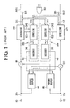
- Fig. 1 is a block diagram showing a known resettable canceller together with associated circuitry, which generally comprises dual, independent input terminals 10 and 12 for respectively receiving horizontally and vertically polarized IF (Intermediate Frequency) signals IFh and IFv, two resetable variable couplers 14 and 16, two subtracters 18 and 20, two demodulators 22 and 24, two control signal generators 26 and 28, an OR gate 30, two output terminals 33 and 35, all of which are coupled as shown.
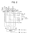
- Each variable coupler (14 or 16) is of a transversal filter type as shown in Fig. 2.
- the control signal generator 26 includes a correlator 32 and an integrator 34, while the other control signal generator 28 similarly includes a correlator 36 and an integrator 38.
- the independent signals IFh and IFv are respectively applied to the input terminals 10, 12 from separate receiving sections (not shown).
- the canceller generally includes the two symmetrical sections arranged for removing contaminating components from the two incoming IF signals, and hence only one symmetrical section will be referred in detail throughout this specification.
- the signal IFh is fed to the variable coupler 14 and also to the subtracter 18.
- the subtracter 18 subtracts the output of the variable coupler 16 from the signal IFh in order to reduce or cancel the components of the other signal IFv deteriorating IFh.
- the subtracter 18 applies the output thereof to the demodulator 22, which produces a digital data signal D1, an error signal E1, a carrier-wave async signal AS1, and a clock signal CK1 reproduced from the recieved IF signal.
- the demodulator 24 produces a digital data signal D2, an error signal E2, a carrier-wave async signal AS2, and a clock signal CK2.
- the error and data signals E1, D2 are correlated, using the clock signal CK1, at the correlator 32 which applies a correction signal 40 to the integrator 34.
- the integrator 34 outputs a control signal 42 which is used to control the variable coupler 16.
- the error and data signals E2, D1 are correlated, using the clock signal CK2, at the correlator 36 which applies a correction signal 44 to the integrator 38.
- the integrator 38 produces a control signal 46 by which the variable coupler 14 is controlled.
- Fig. 2 is a block diagram showing a known transversal filter used as the variable coupler 14 (or 16).
- the transversal filter is a three-tap type for purposes of simplicity. It should be noted that the same device can be utilized in each of the preferred embodiments of this invention.
- the Fig. 2 block diagram which is assumed to be the variable coupler 14 in this instance, comprises an input terminal 50 to which the incoming signal IFh (Fig. 1) is applied, two delay circuits 52 and 54, six tap weighting circuits 56a through 56f, two summing circuits 58 and 60, a 90 o -directional coupler 62 whose output is coupled to the subtracter 20 (Fig. 1), and a controller 64.
- This controller 64 is supplied with the control signal 46 from the integrator 38, and outputs tap coefficient control signals I ⁇ 1, R ⁇ 1, I0, R0, I+1 and R+1 which are respectively applied to the tap weighting circuits 56a-56f.
- the controller 64 also receives the output of the OR gate 30 and is reset in response thereto.
- the operation of the transversal filter shown in Fig. 2 is well known in the art and hence the details thereof will be omitted for brevity.
- the demodulator 22 outputs the carrier-wave async signal AS1 which is applied, via the OR gate 30, to the controller 64 (Fig. 2).
- the controller 64 is responsive to the signal AS1 resetting the tap weighting circuits 56a-56f by allowing each circuit to produce its output with a minimum value. It is clear that when one of the async signals AS1 and AS2 is outputted, both of the variable couplers 14 and 16 are reset.
- the canceller is reset in response to the carrier-wave async signal, the normally operated demodulator of the interferred transmission path tends to be forced into the carrier-wave async state due to the cross-interference before resetting the canceller.
- the canceller is reset and maintained at this state irrespective of the fact that the interfering side demodulator is still able to operate normally.
- the another object of this invention is to provide a cross-polarization interference canceller which is provided with two polarized-signal discriminators each of which is coupled to the corresponding demodulator in order to overcome the difficulty discussed with reference to Fig. 1.
- Still another object of this invention is to provide a cross-polarization interference canceller which enables the demodulator of cross-interfered transmission path to be normally operated until the canceller is reset, and which prolongs the canceller reset as long as the cross-interfering transmission path side demodulator operates normally.
- Still another object of this invention is to provide a cross-polarization interference canceller which includes a high-speed flip-flop for improving the cancellation operation.
- a first aspect of this invention takes the form of a cross-polarization interference canceller for use in a digital radio communications receiver, comprising: first and second variable couplers for receiving respectively first and second IF signals which are orthogonally polarized with respect to each other; a first subtracter to which the first IF signal and the output of the second variable coupler are applied; a second subtracter to which the second IF signal and the output of the first variable coupler are applied; a first demodulator demodulating the output of the first subtracter, and producing first error and data signals; a second demodulator demodulating the output of the second subtracter, and producing second error and data signals; a first control signal generator receiving the first error signal and the second data signal to correlate same, and controlling the second variable coupler; a second control signal generator receiving the second error signal and the first data signal to correlate same, and controlling the first variable coupler; a first polarized-signal discriminator for determining if the first demodulator demodulates the first data signal, and for resetting at least the first
- a second aspect of this invention takes the form of a cross-polarization interference canceller for use in a digital radio communications receiver, comprising: first and second variable couplers for receiving respectively first and second IF signals which are orthogonally polarized with each other; a first subtracter to which the first IF signal and the output of the second variable coupler are applied; a second subtracter to which the second IF signal and the output of the first variable coupler are applied; a first demodulator demodulating the output of the first subtracter, and producing first error and data signals; a second demodulator demodulating the output of the second subtracter, and producing second error and data signals; a first control signal generator receiving the first error signal and the second data signal to correlate same, and controlling the second variable coupler; a second control signal generator receiving the second error signal and the first data signal to correlate same, and controlling the first variable coupler; a first bit error rate detector coupled to the output of the first demodulator, and receiving the first data signal to detect a bit error rate thereof; a first reset signal generator which
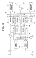
- the cross-polarization interference canceller shown in Fig. 3 is identical to that of Fig. 1 except that the former arrangement further includes two polarized-signal discriminators 70 and 72 which are arranged between the corresponding demodulators and the OR gate 30. Each of the discriminators 70 and 72 has an identical circuit configuration.
- the discriminator 70 has its input and output terminals respectively coupled to the output of demodulator 22 and to the input of the OR gate 30.
- the other discriminator 72 has its input and output terminals respectively coupled to the output of demodulator 24 and to the input of the OR gate 30.
- the polarized-signal discriminator 70 is supplied with the digital data signal D1, and discriminates whether the received signal D1 is in fact the demodulated signal of the incoming IFh. In the event that the received signal D1 is the demodulated signal of IFv instead of IFh, the discriminator 70 produces a reset signal 71 which is applied, via the OR gate 30, to the variable couplers 14 and 16. Similarly, the other discriminator 72 produces a reset signal 73 if the demodulator 24 demodulates the incoming signal IFh instead of IFv. Discriminating the received data signals D1 (or D2), is implemented, by way of example, such that the frame sync signals reproduced at the demodulator 22 and 24 are rendered different. It should be noted that the variable couplers 14 and 16 can concurrently be reset when one of the the demodulators 22, 24 is unable to reproduce the carrier-wave.
- a feature of the first embodiment shown in Fig. 3 is that it can be reset if (a) one incoming IF signal is lowered in level and (b) the cross-polarization interference is high to an extent that the level of the one incoming IF signal is lowered considerably relative to that of the other incoming IF signal at the input of the demodulator provided for the first mentioned incoming IF signal.
- the first embodiment shown in Fig. 3 can be modified such that the discriminators 70 and 72 independently reset the variable couplers 14 and 16 respectively. In this case the OR gate 30 is omitted.
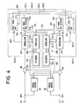
- Fig. 4 show a second embodiment of this invention.
- This second embodiment is identical to that of Fig. 3 except that the former arrangement lacks the polarized-signal discriminators 70 and 72, and, instead thereof, is provided with two bit error rate detectors 50, 54 and two reset signal generators 52, 56, as shown.
- the bit error rate detector 50 receives the data signal D1 from the demodulator 22, and allows its output 62 to assume a logic "1” if the bit error rate exceeds a predetermined value. Otherwise the signal 62 assumes a logic "0".
- the signal 62 is applied to the reset signal generator 52 to which the carrier-wave async signals AS1 and AS2 are also applied.
- Each of the signals AS1 and AS2 assumes a logic "1” when the corresponding demodulator 22 (or 24) is unable to reproduce the carrier wave, and assumes a logic "0" while the corresponding demodulator operates normally.
- each of the reset signals RS1 and RS2 changes its logic value from "1" to "0", respectively.
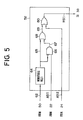
- FIG. 5 is a block diagram showing in detail the reset signal generator 52 (or 54), while Figs. 6 and 7 are timing charts of the signals applied to and derived from the generator 52.
- the reset signal generator 52 comprises a monostable multivibrator 64 to which the signal 62 is applied, an AND gate 66, an OR gate 68 and a NOR gate 80, all of which are coupled as shown.
- the AND gate 66 receives an inverted signal at one input terminal thereof, while receiving the signal AS1 from the demodulator 22 at the other input terminal.
- the NOR gate 80 receives the output signal 69 of the OR gate 68 and the signal AS2 and applies the signal RS1 to the integrator 38.
- the demodulator 24 operates normally.
- the bit error rate becomes high. If the bit error rate increases up to a predetermined value, the signal 62 is allowed to assume a logic "1" (Fig. 6(b)) at time point T1 before the signal AS1 turns to a logic "1".
- the one-shot multivibrator 64 outputs a logic "1" for a predetermined time duration L1 (Fig.
- the integrator 38 is responsive to the reset signal RS1 outputting the control signal 46 which terminates the variable coupler 14 to produce its output.
- the time duration L1 is previously determined to be longer than a time interval L2 shown in Fig. 6(d).
- the time interval L2 is defined from T1 to a time point when the signal AS1 assumes a logic "1" (T2).
- T3 a time point when the signal AS1 assumes a logic "1"
- the reset signal RS1 is maintained at a logic "0" (Fig. 6(g)) in that at this time point the output signal 65 of the monostable multivibrator 64 assumes a logic "0".
- Figs. 6(e) and 6(f) shows timing charts of the signals 67 and 69, respectively.
- variable detector 14 If the variable detector 14 is reset after the demodulator 22 becomes unable to reproduce the carrier-wave as mentioned with reference to the prior art, then there is an undesirable possibility that the normally operated demodulator 24 is rendered incapable of reproducing the carrier-wave. This is because the data signal D1 contains no received information, so that the variable coupler 14 no longer produces an output for cancelling the cross-interference and moreover tends to increase the interference effects.
- variable coupler 14 when the demodulator 22 is unable to reproduce the carrier-wave at time point T3, the variable coupler 14 has already been reset at time point T1 by detecting the bit error rate exceeding the predetermined value. Thus, the difficulty inherent in the prior art can be removed.
- variable coupler 14 restores its normal operation after the predetermined time duration L1. This means that the canceller does not continue to be reset. This advantage is not obtained from the prior art as mentioned previously.
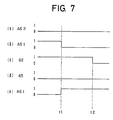
- Fig. 7 shows timing charts which depict another operation of the second embodiment (Figs. 4 and 5) when the incoming signal IFh recovers its normal level. Also in this case it is assumed that the signal AS2 remains a logic "0" (Fig. 7(a)).
- the demodulator 22 begins to reproduce the carrier-wave and hence the logic level of the signal AS1 changes from “1” to "0” at time point t1. Thereafter, the logic level of the signal 62 changes from "1” to "0” at time point t2. Since the signal 65 remains at a logic "0" (Fig.
- the reset signal RS1 changes from a logic "0" to "1" at time point t1 and hence the reset condition is released. Consequently, upon the demodulator 22 restoring normal operation, the canceller begins to function without waiting for the bit error rate to lower. It follows that the arrangement shown in Fig. 4 is able to provide fast convergence.
- the demodulator 24 when the demodulator 24 is brought into a carrier-wave async state while the demodulator 22 operates normally, the signal AS2 changes from a logic "0" to "1". Consequently, the reset signal RS1 assumes a logic "0" and hence resets the variable coupler 14. Thus, the variable coupler 14 ceases to apply its output to the subtracter 20. Resetting the variable coupler 14 under the above circumstances, features fast recovery of the demodulator 24. This is because the output of the variable coupler 14 is unstable until the demodulator 24 restores its normal operation and hence causes a delay of the restoration of the demodulator 24.
- NOR gate 80 can be readily replaced with an OR gate if so desired.
- control signal generators 26, 28 need be adapted to be responsive to a signal of opposite polarity.
- FIG. 8 a third embodiment of this invention is shown in block diagram form. This embodiment is directed to improve the characteristics of the canceller by adding a high-speed flip-flop. This high-speed flip-flop is provided for extracting the error or data signals before correlating them.
- Fig. 8 includes, for purposes of simplicity, only a portion for cancelling the components of the incoming signal IFv which cross-interfers the other signal IFh, and is identical to that of the Fig. 3 arrangment except that a high-speed type flip-flop 100 is added between the correlator 32 and the demodulator 24.
- the correlator 32 includes a flip-flop (not shown) for use in extracting error and data signals to correlate them. Howevever, only low-speed type flip-flops have been employed in the prior art, resulting in the difficulty mentioned below.
- the incoming signals IFh and IFv are independently transmitted through differing path lengths. Therefore, the data transient points of the bit stream reproduced from the signal IFh, are usually different in time from those of the bit stream reproduced from the other signal IFv. Consequently, there is an uncertain time period during which the flip-flop can not extract the error and data signals E1, D2 at the same time. It follows that if the flip-flop provided in the correlator 32 is a slow-speed type, then the uncertain time period becomes large. The possibility that the signals E1 and D2 can not be extracted simultaneously, lessens the cancellation capability.
- Fig. 10 illustrates schematically the uncertain time periods each of which centers around a data transient point, in which Fig. 10(a) is for this invention while Fig. 10(b) is for the prior art.
- the clock signal CK1 is applied to the correlator 32 and also to the high-speed flip-flop 100.
- the data signal D2 is extracted using the clock signal CK1 at the flip-flop 100, and is applied to the correlator 32.
- the correlator 32 extracts the error signal E1 using a relatively slow-speed flip-flop (not shown) using the same clock signal CK1, and then correlates the signals E1 and D2. It is therefore understood that according to the Fig. 8 arrangement, the uncertain time period can be narrowed relative to the case where the signals E1 and D2 are extracted by a slow-speed flip-flop at the correlator 32.
- Fig. 9 is a modification of the arrangement shown in Fig. 8.
- the modification includes the high-speed flip-flop 100 arranged between the demodulator 22 and the correlator 32 in order to extract the error signals E1 using the clock signal CK2. It is clear that this modification has the same effects as the Fig. 8 arrangement.
Landscapes
- Engineering & Computer Science (AREA)
- Computer Networks & Wireless Communication (AREA)
- Signal Processing (AREA)
- Noise Elimination (AREA)
Claims (9)
- Kreuzpolarisationsinterferenz-Löscheinrichtung zur Verwendung in einem digitalen Funkverbindungsempfänger mit:
einem ersten und einem zweiten variablen Koppler (14), (16) zum jeweiligen Empfangen von ersten und zweiten IF-Signalen, die zueinander senkrecht polarisiert sind,
einem ersten Subtrahierer (18), an den das erste IF-Signal und die Ausgabe des zweiten variablen Kopplers angelegt werden,
einem zweiten Subtrahierer (20), an den das zweite IF-Signal und die Ausgabe des ersten variablen Kopplers angelegt werden,
einem ersten Demodulator (22) zum Demodulieren der Ausgabe des ersten Subtrahierers und Erzeugen eines ersten Fehler- und Datensignals (E1, D1),
einem zweiten Demodulator (24) zum Demodulieren der Ausgabe des zweiten Subtrahierers und Erzeugen eines zweiten Fehler- und Datensignals (E2, D2),
einem ersten Steuersignalgenerator (26), der das erste Fehlersignal und das zweite Datensignal empfängt und diese korreliert und den zweiten variablen Koppler steuert,
einem zweiten Steuersignalgenerator (28), der das zweite Fehlersignal und das erste Datensignal empfängt und diese korreliert und den ersten variablen Koppler steuert, gekennzeichnet durch
einen ersten Polarisationssignaldiskriminator (70) zum Bestimmen, ob der erste Demodulator das erste Datensignal demoduliert und zum Zurücksetzen zumindest des ersten variablen Kopplers, wenn der erste Polarisationssignaldiskriminator nicht feststellt, daß der erste Demodulator das erste Datensignal demoduliert, und
einen zweiten Polarisationssignaldiskriminator (72) zum Bestimmen, ob der zweite Demodulator das zweite Datensignal demoduliert und zum Zurücksetzen zumindest des zweiten variablen Kopplers, wenn der zweite Polarisationssignaldiskriminator nicht feststellt, daß der zweite Demodulator das zweite Datensignal demoduliert. - Kreuzpolarisationsinterferenz-Löscheinrichtung nach Anspruch 1, ferner mit einem ODER-Gatter (30), der zwei Eingangsanschlüsse aufweist, die jeweils zum Empfangen der Ausgaben des ersten und zweiten Polarisationssignaldiskriminators verbunden sind, und der einen Ausgangsanschluß aufweist, der zum Anlegen seiner Ausgabe an den ersten und den zweiten variablen Koppler verbunden ist.
- Kreuzpolarisationsinterferenz-Löscheinrichtung zur Verwendung in einem digitalen Funkverbindungsempfänger mit:
einem ersten und einem zweiten variablen Koppler (14), (16) zum jeweiligen Empfangen von ersten und zweiten IF-Signalen, die senkrecht zueinander polarisiert sind,
einem ersten Subtrahierer (18), an den das erste IF-Signal und die Ausgabe des zweiten variablen Kopplers angelegt werden,
einem zweiten Subtrahierer (20), an den das zweite IF-Signal und die Ausgabe des ersten variablen Kopplers angelegt werden,
einem ersten Demodulator (22) zum Demodulieren der Ausgabe des ersten Subtrahierers und Erzeugen eines ersten Fehler- und Datensignals (E1, D1),
einem zweiten Demodulator (24) zum Demodulieren der Ausgabe des zweiten Subtrahierers und Erzeugen eines zweiten Fehler- und Datensignals (E2, D2),
einem ersten Steuersignalgenerator (26) zum Empfangen des ersten Fehlersignals und des zweiten Datensignals zum Korrelieren derselben und Steuern des zweiten variablen Kopplers,
einem zweiten Steuersignalgenerator (28) zum Empfangen des zweiten Fehlersignals und des ersten Datensignals, zum Korrelieren derselben und Steuern des ersten variablen Kopplers, gekennzeichnet durch
einen ersten Bitfehlerrate-Detektor (50), der zum Empfangen des ersten Datensignals (D1) verbunden ist, zum Detektieren dessen erster Bitfehlerrate und Erzeugen einer Ausgabe (62), die einen ersten Pegel annimmt, wenn die erste Bitfehlerrate kleiner als ein erster bestimmter Wert ist, und einen zweiten Pegel annimmt, wenn die erste Bitfehlerrate den ersten bestimmten Wert übersteigt,
einen ersten Rücksetzsignalgenerator (52), der die Ausgabe des ersten Bitfehlerrate-Detektors (50) empfängt, und der außerdem jeweils von dem ersten und dem zweiten Demodulator (22, 24) gelieferte erste und zweite Trägerwellen-Asynchron-Signale (AS1, AS2) empfängt und der ein erstes Rücksetzsignal (RS1) ausgibt, wobei das erste Trägerwellen-Asynchronsignal einen ersten und einen zweiten Pegel annimmt, die jeweils einen Normal- und einen Nichtnormalbetrieb des ersten Demodulators (22) anzeigen, während das zweite Trägerwellen-Asynchronsignal erste und zweite Pegel annimmt, die jeweils einen Normal- und einen Nichtnormalbetrieb des zweiten Demodulators (24) anzeigen, wobei der erste Rücksetzsignalgenerator (52) das erste Rücksetzsignal (RS1) an den zweiten Steuersignalgenerator (28) liefert, der den Betrieb des ersten variablen Kopplers (14) in Abhängigkeit von der Ausgabe des ersten Bitfehlerrate-Detektors (50) beendet, wenn dieser den zweiten Pegel annimmt, und der den ersten variablen Koppler (14) normal weiterarbeiten läßt, in Abhängigkeit von dem ersten Pegel des ersten Trägerwellen-Asynchronsignals (AS1),
einen zweiten Bitfehlerrate-Detektor (54), der zum Empfangen des zweiten Datensignals (D2) verbunden ist, zum Detektieren dessen zweiter Bitfehlerrate und Erzeugen einer Ausgabe, die einen ersten Pegel annimmt, wenn die zweite Bitfehlerrate kleiner als ein zweiter bestimmter Wert ist, und die einen zweiten Pegel annimmt, wenn die zweite Bitfehlerrate den zweiten bestimmten Wert übersteigt und einen zweiten Rücksetzsignalgenerator (56), der die Ausgabe des zweiten Bitfehlerrate-Detektors (54) empfängt und der außerdem die erste und die zweite Trägerwellen-Asynchronsignale (AS1, AS2) empfängt und ein zweites Rücksetzsignal (RS2) ausgibt, wobei der zweite Rücksetzsignalgenerator (56) das zweite Rücksetzsignal (RS2) an den ersten Steuersignalgenerator (26) liefert, der den Betrieb des zweiten variablen Kopplers (16) in Abhängigkeit von der Ausgabe des zweiten Bitfehlerrate-Detektors (54) beendet, wenn dieser den zweiten Pegel annimmt, und der den zweiten variablen Koppler (16) normal weiter arbeiten läßt, in Abhängigkeit von dem ersten Pegel des zweiten Trägerwellen-Asynchronsignals (AS2). - Kreuzpolarisationsinterferenz-Löscheinrichtung nach Anspruch 3, wobei der erste Rücksetzsignalgenerator (52) aufweist:
eine Einrichtung (64), die zum Empfangen der Ausgabe des ersten Bitfehlerrate-Detektors (50) verbunden ist, die die Einrichtung (64) für eine bestimmte Zeitdauer in einen nicht-stabilen Zustand setzt,
ein UND-Gatter (66), das die Ausgabe der Einrichtung (64) und das Trägerwellen-Asynchronsignal (AS1) von dem ersten Demodulator (22) empfängt,
ein ODER-Gatter (68), der die Ausgaben der Einrichtung (64) und des UND-Gatters (66) empfängt und
ein NOR-Gatter (80), der die Ausgabe des ODER-Gatters (68) und das Trägerwellen-Asynchronsignal (AS2) von dem zweiten Demodulator (24) empfängt, wobei die Ausgabe des NOR-Gatters (80) dem ersten Rücksetzsignal (RS1) entspricht. - Kreuzpolarisationsinterferenz-Löschungseinrichtung nach Anspruch 3, wobei der erste Rücksetzsignalgenerator (52) aufweist:
eine Einrichtung (64), die zum Empfangen der Ausgabe des ersten Bitfehlerrate-Detektors (50) verbunden ist, die die Einrichtung (64) für eine bestimmte Zeitdauer in einen nicht-stabilen Zustand setzt,
ein UND-Gatter (66), das die Ausgabe der Einrichtung (64) und das Trägerwellen-Asynchronsignal (AS1) von dem ersten Demodulator (22) empfängt,
ein erstes ODER-Gatter (68), das die Ausgaben der Einrichtung (64) und des UND-Gatters (66) empfängt, und
ein zweites ODER-Gatter, das die Ausgabe des ersten ODER-Gatters (68) und das Trägerwellen-Asynchronsignal (AS2) von dem zweiten Demodulator (24) empfängt, wobei die Ausgabe des zweiten ODER-Gatters dem ersten Rücksetzsignal (RS1) entspricht. - Kreuzpolarisationsinterferenz-Löscheinrichtung nach Anspruch 3, wobei der zweite Rücksetzsignalgenerator (56) aufweist:
eine Einrichtung, die zum Empfangen der Ausgabe des zweiten Bitfehlerrate-Detektors (54) verbunden ist, die die Einrichtung für eine bestimmte Zeitdauer in einen nicht-stabilen Zustand setzt,
ein UND-Gatter, das die Ausgabe der Einrichtung und das Trägerwellen-Asynchronsignal (AS2) von dem zweiten Demodulator (24) empfängt,
ein ODER-Gatter, das die Ausgaben der Einrichtung und des UND-Gatters empfängt, und
ein NOR-Gatter, das die Ausgabe des ODER-Gatters und das Trägerwellen-Asynchronsignal (AS1) von dem ersten Demodulator (22) empfängt, wobei die Ausgabe des NOR-Gatters dem zweiten Rücksetzsignal (RS2) entspricht. - Kreuzpolarisationsinterferenz-Löscheinrichtung nach Anspruch 3, wobei der zweite Rücksetzsignalgenerator (56) aufweist:
eine Einrichtung, die zum Empfangen der Ausgabe des zweiten Bitfehlerrate-Detektors (54) verbunden ist, der die Einrichtung für eine bestimmte Zeitdauer in einen nicht-stabilen Zustand setzt,
ein UND-Gatter, das die Ausgabe der zweiten Einrichtung und das Trägerwellen-Asynchronsignal (AS2) von dem zweiten Demodulator (24) empfängt,
ein erstes ODER-Gatter, das die Ausgaben der Einrichtung und des UND-Gatters empfängt, und
ein zweites ODER-Gatter, das die Ausgabe des ersten ODER-Gatters und das Trägerwellen-Asynchronsignal (AS1) von dem ersten Demodulator (22) empfängt, wobei die Ausgabe des zweiten ODER-Gatters dem zweiten Rücksetzsignal (RS2) entspricht. - Kreuzpolarisationsinterferenz-Löscheinrichtung nach einem der Ansprüche 1 bis 7, ferner mit einem Hochgeschwindigkeits-Flip-Flop (100), das zwischen einem ersten Korrelator (32) des ersten Steuersignalgenerators (26) und dem zweiten Demodulator (24) angeordnet ist, so daß das zweite Datensignal (D2) unter Verwendung des von dem ersten Demodulator (22) gelieferten Taktsignal gewonnen wird.
- Kreuzpolarisationsinterferenz-Löscheinrichtung nach einem der Ansprüche 1 bis 7, ferner mit einem Hochgeschwindigkeits-Flip-Flop (100), das zwischen einem ersten Korrelator (32) des ersten Steuersignalgenerators (26) und dem ersten Demodulator (22) angeordnet ist, so daß das erste Fehlersignal (E1) unter Verwendung eines von dem zweiten Demodulator (24) gelieferten Taktsignal gewonnen wird.
Applications Claiming Priority (6)
| Application Number | Priority Date | Filing Date | Title |
|---|---|---|---|
| JP25289384A JPS61131635A (ja) | 1984-11-30 | 1984-11-30 | 交差偏波干渉除去装置のリセツト方式 |
| JP252893/84 | 1984-11-30 | ||
| JP11573585A JPS61274439A (ja) | 1985-05-29 | 1985-05-29 | 交差偏波干渉除去装置のリセツト方式 |
| JP115735/85 | 1985-05-29 | ||
| JP115736/85 | 1985-05-29 | ||
| JP11573685A JPS61274440A (ja) | 1985-05-29 | 1985-05-29 | 交差偏波干渉除去回路 |
Publications (3)
| Publication Number | Publication Date |
|---|---|
| EP0183274A2 EP0183274A2 (de) | 1986-06-04 |
| EP0183274A3 EP0183274A3 (en) | 1988-01-27 |
| EP0183274B1 true EP0183274B1 (de) | 1991-11-13 |
Family
ID=27313018
Family Applications (1)
| Application Number | Title | Priority Date | Filing Date |
|---|---|---|---|
| EP85115177A Expired - Lifetime EP0183274B1 (de) | 1984-11-30 | 1985-11-29 | Kreuzpolarisationsinterferenzkompensator |
Country Status (4)
| Country | Link |
|---|---|
| US (1) | US4688235A (de) |
| EP (1) | EP0183274B1 (de) |
| CA (1) | CA1253573A (de) |
| DE (1) | DE3584662D1 (de) |
Families Citing this family (20)
| Publication number | Priority date | Publication date | Assignee | Title |
|---|---|---|---|---|
| NL190886C (nl) * | 1986-05-19 | 1994-10-03 | Nippon Telegraph & Telephone | Digitaal signaaldemodulatiesysteem. |
| JPS63272238A (ja) * | 1987-04-30 | 1988-11-09 | Nec Corp | 復調装置 |
| JPS6477235A (en) * | 1987-09-18 | 1989-03-23 | Fujitsu Ltd | Compensating device for interference between cross-polarized waves |
| US4932039A (en) * | 1989-06-08 | 1990-06-05 | The United States Of America As Represented By The Secretary The Navy | Pulse interference canceler of high power out-of-band pulse interference signals |
| CA2022050C (en) * | 1989-07-27 | 1993-03-23 | Toru Matsuura | Cross-polarization interference cancellation system capable of stably carrying out operation |
| JP3225560B2 (ja) * | 1991-11-27 | 2001-11-05 | 日本電気株式会社 | 交差偏波干渉補償装置 |
| US5710799A (en) * | 1992-06-01 | 1998-01-20 | Fujitsu Limited | Cross polarization interference canceler and cross polarization interference eliminating apparatus using the same |
| EP0777341B1 (de) | 1995-11-30 | 2002-02-13 | Loral Aerospace Corporation | Adaptiver Kreuzpolarisationsentzerrer |
| US6268767B1 (en) * | 1999-09-08 | 2001-07-31 | Atmel Corporation | Dual bit error rate estimation in a QAM demodulator |
| US7046753B2 (en) * | 2004-06-29 | 2006-05-16 | Provigent Ltd. | Interference canceller with fast phase adaptation |
| US7613260B2 (en) * | 2005-11-21 | 2009-11-03 | Provigent Ltd | Modem control using cross-polarization interference estimation |
| US7796708B2 (en) * | 2006-03-29 | 2010-09-14 | Provigent Ltd. | Adaptive receiver loops with weighted decision-directed error |
| US7643512B2 (en) | 2006-06-29 | 2010-01-05 | Provigent Ltd. | Cascaded links with adaptive coding and modulation |
| US7839952B2 (en) * | 2006-12-05 | 2010-11-23 | Provigent Ltd | Data rate coordination in protected variable-rate links |
| US7720136B2 (en) | 2006-12-26 | 2010-05-18 | Provigent Ltd | Adaptive coding and modulation based on link performance prediction |
| US8315574B2 (en) | 2007-04-13 | 2012-11-20 | Broadcom Corporation | Management of variable-rate communication links |
| US7821938B2 (en) * | 2007-04-20 | 2010-10-26 | Provigent Ltd. | Adaptive coding and modulation for synchronous connections |
| US8001445B2 (en) * | 2007-08-13 | 2011-08-16 | Provigent Ltd. | Protected communication link with improved protection indication |
| US8040985B2 (en) | 2007-10-09 | 2011-10-18 | Provigent Ltd | Decoding of forward error correction codes in the presence of phase noise |
| GB2474180A (en) * | 2008-07-25 | 2011-04-06 | Smith International | PDC bit having split blades |
Family Cites Families (9)
| Publication number | Priority date | Publication date | Assignee | Title |
|---|---|---|---|---|
| US4112370A (en) * | 1976-08-06 | 1978-09-05 | Signatron, Inc. | Digital communications receiver for dual input signal |
| US4100376A (en) * | 1977-01-03 | 1978-07-11 | Raytheon Company | Pilot tone demodulator |
| CA1112300A (en) * | 1978-01-23 | 1981-11-10 | Gerald J.P. Lo | Circuit and method for reducing polarization crosstalk caused by rainfall |
| US4220923A (en) * | 1978-03-29 | 1980-09-02 | Harris Corporation | Adaptive interference reduction system for crosstalk cancellation in a dual polarization system |
| US4321705A (en) * | 1979-03-02 | 1982-03-23 | Nippon Electronics Co., Ltd. | Digital equalizer for a cross-polarization receiver |
| US4479258A (en) * | 1981-09-30 | 1984-10-23 | Nippon Electric Co., Ltd. | Cross-polarization crosstalk canceller |
| US4438530A (en) * | 1982-06-14 | 1984-03-20 | Bell Telephone Laboratories, Incorporated | Adaptive cross-polarization interference cancellation system |
| CA1215430A (en) * | 1982-12-20 | 1986-12-16 | Toshihiko Ryu | Cross-polarization distortion canceller for use in digital radio communication receiver |
| US4577330A (en) * | 1984-04-19 | 1986-03-18 | At&T Bell Laboratories | Cross-polarization interference cancellation arrangement for digital radio channels |
-
1985
- 1985-11-27 US US06/803,132 patent/US4688235A/en not_active Expired - Lifetime
- 1985-11-29 EP EP85115177A patent/EP0183274B1/de not_active Expired - Lifetime
- 1985-11-29 DE DE8585115177T patent/DE3584662D1/de not_active Expired - Lifetime
- 1985-11-29 CA CA000496504A patent/CA1253573A/en not_active Expired
Also Published As
| Publication number | Publication date |
|---|---|
| CA1253573A (en) | 1989-05-02 |
| EP0183274A2 (de) | 1986-06-04 |
| US4688235A (en) | 1987-08-18 |
| DE3584662D1 (de) | 1991-12-19 |
| EP0183274A3 (en) | 1988-01-27 |
Similar Documents
| Publication | Publication Date | Title |
|---|---|---|
| EP0183274B1 (de) | Kreuzpolarisationsinterferenzkompensator | |
| US5075697A (en) | Dual polarization transmission system | |
| EP0307950B1 (de) | Kreuzpolarisationsinterferenzkompensator | |
| EP0315990B1 (de) | Interferenzkompensator und Verfahren zur Kompensation einer Interferenz | |
| EP0216141B1 (de) | Kombinierte Kreuzpolarisationsinterferenzkompensation und Intersymbolinterferenzentzerrung für erdgebundene digitale Funksysteme | |
| US5327458A (en) | Automatic equalizer capable of effectively cancelling intersymbol interference and cross polarization interference in co-channel dual polarization | |
| JPS6412136B2 (de) | ||
| US4803438A (en) | 8-phase phase-shift keying demodulator | |
| JPS6350231A (ja) | 通信システムとこれに用いる受信装置 | |
| GB2314488A (en) | MRC diversity circuit uses branch with maximum RSSI | |
| JP2569665B2 (ja) | 2偏波ディジタル復調方式 | |
| JPH04150320A (ja) | ダイバシティ受信装置 | |
| JP2669235B2 (ja) | 交差偏波干渉補償装置 | |
| JPH0436614B2 (de) | ||
| JP2526475B2 (ja) | 交差偏波間干渉除去器付復調装置 | |
| JPH01125135A (ja) | 交差偏波間干渉補償装置 | |
| JP2580015B2 (ja) | 交差偏波間干渉補償装置 | |
| JP2680373B2 (ja) | 交差偏波間干渉補償装置 | |
| JP2560339B2 (ja) | ディジタル復調装置 | |
| JP2674399B2 (ja) | 交差偏波干渉除去装置 | |
| JP2504184B2 (ja) | 直交偏波通信方式 | |
| CA2164018C (en) | Adaptive cross-polarization equalizer | |
| JPH0548567A (ja) | デイジタル多重無線方式 | |
| JPH04286234A (ja) | 交差偏波干渉除去回路 | |
| JPH05122189A (ja) | 交差偏波間干渉除去装置 |
Legal Events
| Date | Code | Title | Description |
|---|---|---|---|
| PUAI | Public reference made under article 153(3) epc to a published international application that has entered the european phase |
Free format text: ORIGINAL CODE: 0009012 |
|
| 17P | Request for examination filed |
Effective date: 19851129 |
|
| AK | Designated contracting states |
Kind code of ref document: A2 Designated state(s): DE FR IT |
|
| PUAL | Search report despatched |
Free format text: ORIGINAL CODE: 0009013 |
|
| AK | Designated contracting states |
Kind code of ref document: A3 Designated state(s): DE FR IT |
|
| 17Q | First examination report despatched |
Effective date: 19900629 |
|
| GRAA | (expected) grant |
Free format text: ORIGINAL CODE: 0009210 |
|
| AK | Designated contracting states |
Kind code of ref document: B1 Designated state(s): DE FR IT |
|
| REF | Corresponds to: |
Ref document number: 3584662 Country of ref document: DE Date of ref document: 19911219 |
|
| ET | Fr: translation filed | ||
| ITF | It: translation for a ep patent filed | ||
| PLBE | No opposition filed within time limit |
Free format text: ORIGINAL CODE: 0009261 |
|
| STAA | Information on the status of an ep patent application or granted ep patent |
Free format text: STATUS: NO OPPOSITION FILED WITHIN TIME LIMIT |
|
| 26N | No opposition filed | ||
| PGFP | Annual fee paid to national office [announced via postgrant information from national office to epo] |
Ref country code: FR Payment date: 20021108 Year of fee payment: 18 |
|
| PGFP | Annual fee paid to national office [announced via postgrant information from national office to epo] |
Ref country code: DE Payment date: 20021205 Year of fee payment: 18 |
|
| PG25 | Lapsed in a contracting state [announced via postgrant information from national office to epo] |
Ref country code: DE Free format text: LAPSE BECAUSE OF NON-PAYMENT OF DUE FEES Effective date: 20040602 |
|
| PG25 | Lapsed in a contracting state [announced via postgrant information from national office to epo] |
Ref country code: FR Free format text: LAPSE BECAUSE OF NON-PAYMENT OF DUE FEES Effective date: 20040730 |
|
| REG | Reference to a national code |
Ref country code: FR Ref legal event code: ST |