EP0181149B1 - Matériaux de contact pour interrupteurs à vide - Google Patents
Matériaux de contact pour interrupteurs à vide Download PDFInfo
- Publication number
- EP0181149B1 EP0181149B1 EP85307859A EP85307859A EP0181149B1 EP 0181149 B1 EP0181149 B1 EP 0181149B1 EP 85307859 A EP85307859 A EP 85307859A EP 85307859 A EP85307859 A EP 85307859A EP 0181149 B1 EP0181149 B1 EP 0181149B1
- Authority
- EP
- European Patent Office
- Prior art keywords
- contact material
- prepared
- breaking performance
- samples
- contact
- Prior art date
- Legal status (The legal status is an assumption and is not a legal conclusion. Google has not performed a legal analysis and makes no representation as to the accuracy of the status listed.)
- Expired
Links
- 239000000463 material Substances 0.000 title claims description 71
- 239000010955 niobium Substances 0.000 claims description 48
- 238000000034 method Methods 0.000 claims description 37
- 229910052750 molybdenum Inorganic materials 0.000 claims description 26
- 239000010949 copper Substances 0.000 claims description 23
- 239000000843 powder Substances 0.000 claims description 20
- 229910052758 niobium Inorganic materials 0.000 claims description 18
- 229910052802 copper Inorganic materials 0.000 claims description 17
- 238000005245 sintering Methods 0.000 claims description 11
- 230000008595 infiltration Effects 0.000 claims description 10
- 238000001764 infiltration Methods 0.000 claims description 10
- 229910052715 tantalum Inorganic materials 0.000 claims description 10
- RYGMFSIKBFXOCR-UHFFFAOYSA-N Copper Chemical compound [Cu] RYGMFSIKBFXOCR-UHFFFAOYSA-N 0.000 claims description 7
- 239000011733 molybdenum Substances 0.000 claims description 7
- ZOKXTWBITQBERF-UHFFFAOYSA-N Molybdenum Chemical compound [Mo] ZOKXTWBITQBERF-UHFFFAOYSA-N 0.000 claims description 6
- GUCVJGMIXFAOAE-UHFFFAOYSA-N niobium atom Chemical compound [Nb] GUCVJGMIXFAOAE-UHFFFAOYSA-N 0.000 claims description 4
- GUVRBAGPIYLISA-UHFFFAOYSA-N tantalum atom Chemical compound [Ta] GUVRBAGPIYLISA-UHFFFAOYSA-N 0.000 claims description 4
- 229910045601 alloy Inorganic materials 0.000 claims 1
- 239000000956 alloy Substances 0.000 claims 1
- 239000002131 composite material Substances 0.000 claims 1
- 229910000765 intermetallic Inorganic materials 0.000 claims 1
- 239000000126 substance Substances 0.000 claims 1
- 239000000523 sample Substances 0.000 description 14
- 229910017813 Cu—Cr Inorganic materials 0.000 description 10
- 239000011651 chromium Substances 0.000 description 5
- 229910052804 chromium Inorganic materials 0.000 description 4
- 239000000203 mixture Substances 0.000 description 4
- 239000011812 mixed powder Substances 0.000 description 3
- 238000004663 powder metallurgy Methods 0.000 description 3
- 239000013074 reference sample Substances 0.000 description 3
- UFHFLCQGNIYNRP-UHFFFAOYSA-N Hydrogen Chemical compound [H][H] UFHFLCQGNIYNRP-UHFFFAOYSA-N 0.000 description 2
- 229910052739 hydrogen Inorganic materials 0.000 description 2
- 239000001257 hydrogen Substances 0.000 description 2
- 238000005259 measurement Methods 0.000 description 2
- OKTJSMMVPCPJKN-UHFFFAOYSA-N Carbon Chemical compound [C] OKTJSMMVPCPJKN-UHFFFAOYSA-N 0.000 description 1
- BQCADISMDOOEFD-UHFFFAOYSA-N Silver Chemical compound [Ag] BQCADISMDOOEFD-UHFFFAOYSA-N 0.000 description 1
- 229910052799 carbon Inorganic materials 0.000 description 1
- 238000002844 melting Methods 0.000 description 1
- 230000008018 melting Effects 0.000 description 1
- 238000002360 preparation method Methods 0.000 description 1
- 229910052709 silver Inorganic materials 0.000 description 1
- 239000004332 silver Substances 0.000 description 1
- 229910052721 tungsten Inorganic materials 0.000 description 1
- 239000010937 tungsten Substances 0.000 description 1
Images


Classifications
-
- H—ELECTRICITY
- H01—ELECTRIC ELEMENTS
- H01H—ELECTRIC SWITCHES; RELAYS; SELECTORS; EMERGENCY PROTECTIVE DEVICES
- H01H1/00—Contacts
- H01H1/02—Contacts characterised by the material thereof
- H01H1/0203—Contacts characterised by the material thereof specially adapted for vacuum switches
Definitions
- the present invention relates to vacuum circuit breakers which are excellent in high current breaking characteristics, and more particularly, it relates to contact materials for vacuum circuit breakers.
- Vacuum circuit breakers which are maintenance-free, pollution-free and excellent in breaking performance, have been widely used in the art. However, the art is awaiting development of circuit breakers applicable to both higher voltages and higher currents.
- a vacuum circuit breaker depends mainly upon its contact material.
- a contact material preferably has (1) large breaking capacity, (2) high withstanding voltage, (3) low contact resistance, (4) a requirement for a small force to separate welded contacts, (5) small contact consumption, (6) small chopping current, (7) good machinability and (8) good mechanical strength.
- a contact material having all of these preferred characteristics it is only those particularly important characteristics required for a specific use for which improvements are sought at the sacrifice of the other characteristics.
- a copper (Cu)-tungsten (W) contact material as disclosed in Japanese Patent Laying-Open Gazette No. 78429/1980 is excellent in withstanding voltage performance, and thus commonly applied to load switches and contactors.
- the Cu-W contact material is not as satisfactory in current breaking performance.
- a copper (Cu)-chromium (Cr) contact material disclosed in, e.g., Japanese Patent Laying-Open Gazette No. 71375/1979 is remarkably superior in breaking performance, and thus commonly applied to circuit breakers.
- the Cu-Cr contact material is inferior in withstanding voltage performance to the Cu-W contact material.
- contact materials generally used in air or oil are described in the literature such as "General Lecture of Powder Metallurgy” edited by Yoshiharu Matsuyama et al. and published (1972) by Nikkan Kogyo Shinbun.
- contact materials as silver (Ag)-molybdenum (Mo) and Cu-Mo systems as described in "General Lecture of Powder Metallurgy” pp. 229-230 are inferior in withstanding voltage performance to the Cu-W contact material as well as in current breaking performance to the Cu-Cr contact material, and thus are at present hardly ever applied to vacuum circuit breakers.
- the present invention seeks to provide contact materials for vacuum circuit breakers which exhibit excellent breaking performance with improvements in characteristics.
- the contact materials for vacuum circuit breakers according to the present invention comprise (1) copper, (2) molybdenum and (3) niobium (Nb) or tantalum (Ta).
- Three sample groups of contact materials were prepared by three methods of applied powder metallurgy, i.e., an infiltration method, a powder sintering method and a hot press method.
- Mo powder of 3 um mean grain size, Nb powder of grain size less than 40 ⁇ m and Cu powder of grain size less than 40 ⁇ .1m were mixed in the weight ratio of 75.7:7.8:16.5 for two hours.
- the mixed powder was then filled into dies of prescribed geometry, to be compacted by a press under a pressure of 1 ton/cm 2 .
- the compact thus formed was sintered at 1000°C for two hours in a vacuum, to obtain loosely sintered compact.
- a block of oxygen-free copper was placed on the loosely sintered compact, which were then kept at 1250°C for one hour in a hydrogen atmosphere, to obtain a contact material impregnated with oxygen-free copper.
- the final composition of this contact material was that of a sample 2N as shown in Table 1A.
- Table 1A lists the samples of the Cu-Mo-Nb system prepared by the infiltration method, in which a sample 1 Reference containing no Nb was prepared for reference.
- Table 1B shows samples of the Cu-Mo-Ta system prepared by the infiltration method under the same processing conditions.
- Mo powder of 3 pm mean grain size, Nb powder of grain size less than 40 pm and Cu powder of grain size less than 75 ⁇ m were mixed in the weight ratio 38.1:1.9:60 for two hours.
- the mixed powder was then filled into dies of prescribed geometry, to be compacted by a press under a pressure of 3.3 ton/cm2.
- the compact thus formed was sintered in a hydrogen atmosphere at a temperature just below the melting point of copper for two hours, to obtain a contact material.
- This contact material is shown as a sample 17N in Table 2A, which lists the samples of the Cu-Mo-Nb system obtained by the powder sintering method.
- a sample 16 Reference containing no Nb and a sample 23 Reference of the Cu-Cr system are shown for reference.
- Table 2B shows samples of the Cu-Mo-Ta system prepared by the powder sintering method. These samples were prepared under the same conditions as those for the Cu-Mo-Nb system contact material.
- the contact material thus obtained is shown as a sample 25N in Table 3A, which lists the samples of the Cu-Mo-Nb system prepared by the hot press method.
- a sample 24 Reference containing no Nb was prepared for reference.
- Table 3B shows samples of the Cu-Mo-Ta system prepared by the hot press method. Conditions for preparing these samples were identical to those for the samples of the Cu-Mo-Nb system.
- Fig. 1A shows normalized breaking performance of the samples prepared by the infiltration method as shown in Table 1A.
- the contact materials according to the present invention are of the ternary system, and hence the abscissa indicates the content of Nb with respect to Mo, i.e., the total weight percentage of Mo and Nb is 100%.
- the ordinate indicates the normalized breaking performance with reference to the conventional Cu-50 wt.% Mo contact material, i.e., the value of the current breakable through the standard vacuum circuit breaker, with reference to the Cu-50 wt.% Mo contact material as shown by a double circle 4 in Fig. 1A.
- Curve 1 in Fig. 1A represents breaking performance of the Cu-Mo-Nb samples 2N and 3N respectively containing about 60 wt.% Cu as shown in Table 1A.
- Curve 2 represents breaking performance of the Cu-Mo-Nb samples 4N, 5N, 6N, 8N and 9N respectively containing about 50 wt.% Cu and the Cu-50.2 wt.% Mo sample 1R containing no Nb as shown in Table 1A.
- Curve 3 in Fig. 1A represents breaking performance of the Cu-Mo-Nb samples 10N, 11N, 12N, 13N, 14N and 15N respectively containing about 40 wt.% Cu as shown in Table 1A.
- Line 5 in Fig. 1A represents breaking performance of the sample 23R of the conventional Cu-25 wt.% Cr contact material prepared by the powder sintering method for reference.
- Fig. 1 B shows breaking performance of the Cu-Mo-Ta contact material prepared by the infiltration method as shown in Table 18.
- the contact materials of the Cu-Mo-Nb and Cu-Mo-Ta systems prepared by the infiltration method are superior in breaking performance to the conventional Cu-Cr contact material.
- the samples were prepared within the range of 2.441.4 wt.% Nb and 15.557.2 wt.% Mo, or 4.4-54.0 wt.% Ta and 5.054.7 wt.% Mo.
- contents of Mo and Nb, or Mo and Ta may be in wider ranges.
- increase in the contents of Ta, Nb and Mo generally involves increased cost and reduced machinability. Therefore, optimum compositions can be selected in consideration of electrical characteristics as well as cost and mechanical characteristics.
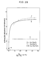
- Fig. 2A shows normalized breaking performance of the Cu-Mo-Nb samples prepared by the powder sintering method as listed in Table 2A.
- the abscissa indicates the Nb content with respect to Mo similar to Fig. 1A, while the ordinate indicates the breaking performance with reference to a contact material of Cu-25 wt.% Mo (sample 16R) as shown by a double circle 8.
- Curve 6 represents breaking performance of samples 20N, 21N, 22N and 23N of the Cu-Mo-Nb contact material respectively containing about 75 wt.% Cu and the reference sample 16R as shown in Table 2A.
- FIG. 2A represents breaking performance of the samples 17N, 18N and 19N of the Cu-Mo-Nb system respectively containing about 60 wt.% as shown in Table 2A.
- Line 5 in Fig. 2A represents breaking performance of conventional Cu-25 wt.% Cr contact material for reference, similar to Fig. 1A.
- Fig. 2B shows breaking performance of the Cu-Mo-Ta contact material prepared by the powder sintering method as shown in Table 2B.
- the contact materials of the Cu-Mo-Nb and Cu-Mo-Ta systems prepared by the powder sintering method are also superior in breaking performance to the conventional Cu-Cr contact material. While compositions of the contact materials prepared by the powder sintering method were within the ranges of 1.2-11.4 wt.% Nb and 1.7938.1 wt.% Mo, or 2.2-11.0 wt.% Ta and 1.40-36.5 wt.% Mo, the contact materials in wider ranges of these contents are believed to be superior in breaking performance to the conventional Cu-Cr contact material.
- Fig. 3A shows breaking performance of the contact material prepared by the hot press method as shown in Table 3A. Similar to Fig. 1A, the abscissa indicates the Nb content with respect to Mo. The ordinate indicates the breaking performance with reference to a contact material of Cu - 25 wt.% Mo (sample 24R) prepared by the hot press method, with the reference being shown by a double circle 11.
- Curve 9 in Fig. 3A represents the breaking performance of the Cu ⁇ Mo ⁇ Nb samples 28N, 29N and 30N respectively containing about 75 wt.% Cu and the reference sample 24R as shown in Table 3A.
- Curve 10 represents the breaking performance of samples 25N, 26N and 27N respectively containing about 60 wt.% Cu as shown in Table 3A. Similar to Fig. 1A, line 5 represents the breaking performance of the conventional contact material of Cu - 25 wt.% Cr (sample 23R) for reference.
- Fig. 3B shows breaking performance of the Cu-Mo-Ta contact material prepared by the hot press method as shown in Table 3B.
- the contact materials of the Cu-Mo-Nb and Cu-Mo-Ta systems prepared by the hot press method are also superior in breaking performance to the conventional Cu-Cr contact material. Similar to Tables 2A and 2B, compositions of the contact material prepared by the hot press method were within the ranges of 1.2-11.4 wt.% Nb and 17.938.1 wt.% Mo, or 2.2-11.0 wt.% Ta and 14.036.5 wt.% Mo, but the contact materials of these systems in wider ranges of the contents are believed to be superior in breaking performance to the conventional Cu-Cr contact. material.
- the Cu-Mo-Nb samples containing 40 wt.% Cu are lower in breaking performance in certain ranges of the Mo and Nb contents than the other Cu-Mo-Nb samples in Fig. 1A, they are sufficiently applicable in practice since the breaking performance increases with increase of the Nb content.
Claims (7)
Applications Claiming Priority (4)
| Application Number | Priority Date | Filing Date | Title |
|---|---|---|---|
| JP23061984A JPS61107619A (ja) | 1984-10-30 | 1984-10-30 | 真空しや断器用接点 |
| JP230619/84 | 1984-10-30 | ||
| JP24751784A JPS61124013A (ja) | 1984-11-20 | 1984-11-20 | 真空しや断器用接点 |
| JP247517/84 | 1984-11-20 |
Publications (3)
| Publication Number | Publication Date |
|---|---|
| EP0181149A2 EP0181149A2 (fr) | 1986-05-14 |
| EP0181149A3 EP0181149A3 (en) | 1987-07-29 |
| EP0181149B1 true EP0181149B1 (fr) | 1990-01-03 |
Family
ID=26529442
Family Applications (1)
| Application Number | Title | Priority Date | Filing Date |
|---|---|---|---|
| EP85307859A Expired EP0181149B1 (fr) | 1984-10-30 | 1985-10-30 | Matériaux de contact pour interrupteurs à vide |
Country Status (3)
| Country | Link |
|---|---|
| US (1) | US4626282A (fr) |
| EP (1) | EP0181149B1 (fr) |
| DE (1) | DE3575234D1 (fr) |
Families Citing this family (13)
| Publication number | Priority date | Publication date | Assignee | Title |
|---|---|---|---|---|
| CN1003329B (zh) * | 1984-12-13 | 1989-02-15 | 三菱电机有限公司 | 真空断路器用触头 |
| KR900001613B1 (ko) * | 1986-01-10 | 1990-03-17 | 미쯔비시 덴끼 가부시기가이샤 | 진공차단기용 접점재료 |
| US5170244A (en) * | 1986-03-06 | 1992-12-08 | Kabushiki Kaisha Toshiba | Electrode interconnection material, semiconductor device using this material and driving circuit substrate for display device |
| EP0236629B1 (fr) * | 1986-03-06 | 1994-05-18 | Kabushiki Kaisha Toshiba | Circuit de commande d'un dispositif d'affichage à cristaux liquides |
| US4788627A (en) * | 1986-06-06 | 1988-11-29 | Tektronix, Inc. | Heat sink device using composite metal alloy |
| JPS6362122A (ja) * | 1986-09-03 | 1988-03-18 | 株式会社日立製作所 | 真空遮断器用電極の製造法 |
| EP0264626A3 (fr) * | 1986-10-17 | 1988-12-28 | Battelle-Institut e.V. | Procédé de fabrication d'alliages à base de cuivre, renforcés par dispersion |
| US5252147A (en) * | 1989-06-15 | 1993-10-12 | Iowa State University Research Foundation, Inc. | Modification of surface properties of copper-refractory metal alloys |
| JP3441331B2 (ja) * | 1997-03-07 | 2003-09-02 | 芝府エンジニアリング株式会社 | 真空バルブ用接点材料の製造方法 |
| US5903203A (en) * | 1997-08-06 | 1999-05-11 | Elenbaas; George H. | Electromechanical switch |
| DE19903619C1 (de) * | 1999-01-29 | 2000-06-08 | Louis Renner Gmbh | Pulvermetallurgisch hergestellter Verbundwerkstoff und Verfahren zu dessen Herstellung sowie dessen Verwendung |
| JP6090388B2 (ja) * | 2015-08-11 | 2017-03-08 | 株式会社明電舎 | 電極材料及び電極材料の製造方法 |
| KR101938488B1 (ko) * | 2017-08-03 | 2019-01-14 | 서울대학교산학협력단 | 내화 금속계 합금과 구리의 이중연속구조 복합재 및 그 제조방법 |
Family Cites Families (8)
| Publication number | Priority date | Publication date | Assignee | Title |
|---|---|---|---|---|
| GB1079013A (en) * | 1964-04-21 | 1967-08-09 | English Electric Co Ltd | Improvements in or relating to contacts and electrodes |
| GB1346758A (en) * | 1970-02-24 | 1974-02-13 | Ass Elect Ind | Vacuum interrupter contacts |
| CA1084565A (fr) * | 1976-07-21 | 1980-08-26 | James M. Lafferty | Commutateur a vide pour courant intense avec erosion reduite des contacts |
| JPS58165225A (ja) * | 1982-03-26 | 1983-09-30 | 株式会社日立製作所 | 真空しや断器 |
| US4517033A (en) * | 1982-11-01 | 1985-05-14 | Mitsubishi Denki Kabushiki Kaisha | Contact material for vacuum circuit breaker |
| DE3362624D1 (en) * | 1982-11-16 | 1986-04-24 | Mitsubishi Electric Corp | Contact material for vacuum circuit breaker |
| JPS6054124A (ja) * | 1983-09-02 | 1985-03-28 | 株式会社日立製作所 | 真空しや断器 |
| JPS59163726A (ja) * | 1983-03-04 | 1984-09-14 | 株式会社日立製作所 | 真空しや断器 |
-
1985
- 1985-10-30 US US06/792,983 patent/US4626282A/en not_active Expired - Lifetime
- 1985-10-30 EP EP85307859A patent/EP0181149B1/fr not_active Expired
- 1985-10-30 DE DE8585307859T patent/DE3575234D1/de not_active Expired - Fee Related
Also Published As
| Publication number | Publication date |
|---|---|
| US4626282A (en) | 1986-12-02 |
| DE3575234D1 (de) | 1990-02-08 |
| EP0181149A3 (en) | 1987-07-29 |
| EP0181149A2 (fr) | 1986-05-14 |
Similar Documents
| Publication | Publication Date | Title |
|---|---|---|
| EP0181149B1 (fr) | Matériaux de contact pour interrupteurs à vide | |
| EP2081200B1 (fr) | Contact électrique pour interrupteur sous vide | |
| EP0227973B1 (fr) | Matériau pour le contact d'une électrode pour un interrupteur à vide et méthode de fabrication d'un tel matériau | |
| EP0101024B1 (fr) | Matériau de contact pour interrupteur à vide et son procédé de fabrication | |
| US5429656A (en) | Silver-based contact material for use in power engineering switchgear | |
| US4870231A (en) | Contact for vacuum interrupter | |
| EP0414709B1 (fr) | Materiau fritte de contact a base d'argent utilise dans des appareils commutateurs d'energie, notamment des plots de contact de commutateurs a basse tension | |
| EP0610018B1 (fr) | Matériau de contact pour un interrupteur à vide | |
| EP0609601B1 (fr) | Matériel de contact pour interrupteur à vide et procédé pour sa fabrication | |
| AU619078B2 (en) | Ag-sno electrical contact materials and manufacturing method thereof | |
| EP0118844A2 (fr) | Interrupteur à vide et méthode de sa fabrication | |
| US5972068A (en) | Contact material for vacuum valve | |
| US4687515A (en) | Vacuum interrupter contact | |
| JPS63118032A (ja) | 真空しや断器用接点材料 | |
| EP0365043B1 (fr) | Matériau pour électrodes de contact des disjoncteurs à vide | |
| JP2003223834A (ja) | 電気接点部材とその製法 | |
| JP2661199B2 (ja) | 真空インタラプタの電極材料 | |
| EP0440340A2 (fr) | Matériaux pour contacts électriques et leur procédé de fabrication | |
| JP2661201B2 (ja) | 真空インタラプタの電極材料 | |
| JP2661202B2 (ja) | 真空インタラプタの電極材料 | |
| JP2661200B2 (ja) | 真空インタラプタの電極材料 | |
| JPH09306268A (ja) | 真空バルブ用接点材料 | |
| JPH0157457B2 (fr) | ||
| JPH02809B2 (fr) | ||
| JPH0145171B2 (fr) |
Legal Events
| Date | Code | Title | Description |
|---|---|---|---|
| PUAI | Public reference made under article 153(3) epc to a published international application that has entered the european phase |
Free format text: ORIGINAL CODE: 0009012 |
|
| AK | Designated contracting states |
Kind code of ref document: A2 Designated state(s): DE FR GB IT SE |
|
| PUAL | Search report despatched |
Free format text: ORIGINAL CODE: 0009013 |
|
| AK | Designated contracting states |
Kind code of ref document: A3 Designated state(s): DE FR GB IT SE |
|
| 17P | Request for examination filed |
Effective date: 19870814 |
|
| 17Q | First examination report despatched |
Effective date: 19890110 |
|
| GRAA | (expected) grant |
Free format text: ORIGINAL CODE: 0009210 |
|
| AK | Designated contracting states |
Kind code of ref document: B1 Designated state(s): DE FR GB IT SE |
|
| REF | Corresponds to: |
Ref document number: 3575234 Country of ref document: DE Date of ref document: 19900208 |
|
| ITF | It: translation for a ep patent filed |
Owner name: MODIANO & ASSOCIATI S.R.L. |
|
| ET | Fr: translation filed | ||
| PLBE | No opposition filed within time limit |
Free format text: ORIGINAL CODE: 0009261 |
|
| STAA | Information on the status of an ep patent application or granted ep patent |
Free format text: STATUS: NO OPPOSITION FILED WITHIN TIME LIMIT |
|
| 26N | No opposition filed | ||
| ITTA | It: last paid annual fee | ||
| EAL | Se: european patent in force in sweden |
Ref document number: 85307859.0 |
|
| REG | Reference to a national code |
Ref country code: GB Ref legal event code: 746 Effective date: 19951026 |
|
| REG | Reference to a national code |
Ref country code: FR Ref legal event code: D6 |
|
| ITPR | It: changes in ownership of a european patent |
Owner name: OFFERTA DI LICENZA AL PUBBLICO |
|
| PGFP | Annual fee paid to national office [announced via postgrant information from national office to epo] |
Ref country code: SE Payment date: 19961016 Year of fee payment: 12 |
|
| PG25 | Lapsed in a contracting state [announced via postgrant information from national office to epo] |
Ref country code: SE Free format text: LAPSE BECAUSE OF NON-PAYMENT OF DUE FEES Effective date: 19971031 |
|
| EUG | Se: european patent has lapsed |
Ref document number: 85307859.0 |
|
| PGFP | Annual fee paid to national office [announced via postgrant information from national office to epo] |
Ref country code: GB Payment date: 20011031 Year of fee payment: 17 |
|
| REG | Reference to a national code |
Ref country code: GB Ref legal event code: IF02 |
|
| PGFP | Annual fee paid to national office [announced via postgrant information from national office to epo] |
Ref country code: FR Payment date: 20021008 Year of fee payment: 18 |
|
| PG25 | Lapsed in a contracting state [announced via postgrant information from national office to epo] |
Ref country code: GB Free format text: LAPSE BECAUSE OF NON-PAYMENT OF DUE FEES Effective date: 20021030 |
|
| PGFP | Annual fee paid to national office [announced via postgrant information from national office to epo] |
Ref country code: DE Payment date: 20021031 Year of fee payment: 18 |
|
| GBPC | Gb: european patent ceased through non-payment of renewal fee | ||
| PG25 | Lapsed in a contracting state [announced via postgrant information from national office to epo] |
Ref country code: DE Free format text: LAPSE BECAUSE OF NON-PAYMENT OF DUE FEES Effective date: 20040501 |
|
| PG25 | Lapsed in a contracting state [announced via postgrant information from national office to epo] |
Ref country code: FR Free format text: LAPSE BECAUSE OF NON-PAYMENT OF DUE FEES Effective date: 20040630 |
|
| REG | Reference to a national code |
Ref country code: FR Ref legal event code: ST |