EP0178660B1 - X-ray exposure apparatus - Google Patents
X-ray exposure apparatus Download PDFInfo
- Publication number
- EP0178660B1 EP0178660B1 EP85113171A EP85113171A EP0178660B1 EP 0178660 B1 EP0178660 B1 EP 0178660B1 EP 85113171 A EP85113171 A EP 85113171A EP 85113171 A EP85113171 A EP 85113171A EP 0178660 B1 EP0178660 B1 EP 0178660B1
- Authority
- EP
- European Patent Office
- Prior art keywords
- gas
- attenuation chamber
- less
- mask
- ray
- Prior art date
- Legal status (The legal status is an assumption and is not a legal conclusion. Google has not performed a legal analysis and makes no representation as to the accuracy of the status listed.)
- Expired - Lifetime
Links
Images

Classifications
-
- H10P95/00—
-
- B—PERFORMING OPERATIONS; TRANSPORTING
- B82—NANOTECHNOLOGY
- B82Y—SPECIFIC USES OR APPLICATIONS OF NANOSTRUCTURES; MEASUREMENT OR ANALYSIS OF NANOSTRUCTURES; MANUFACTURE OR TREATMENT OF NANOSTRUCTURES
- B82Y10/00—Nanotechnology for information processing, storage or transmission, e.g. quantum computing or single electron logic
-
- G—PHYSICS
- G03—PHOTOGRAPHY; CINEMATOGRAPHY; ANALOGOUS TECHNIQUES USING WAVES OTHER THAN OPTICAL WAVES; ELECTROGRAPHY; HOLOGRAPHY
- G03F—PHOTOMECHANICAL PRODUCTION OF TEXTURED OR PATTERNED SURFACES, e.g. FOR PRINTING, FOR PROCESSING OF SEMICONDUCTOR DEVICES; MATERIALS THEREFOR; ORIGINALS THEREFOR; APPARATUS SPECIALLY ADAPTED THEREFOR
- G03F7/00—Photomechanical, e.g. photolithographic, production of textured or patterned surfaces, e.g. printing surfaces; Materials therefor, e.g. comprising photoresists; Apparatus specially adapted therefor
- G03F7/20—Exposure; Apparatus therefor
- G03F7/2037—Exposure with X-ray radiation or corpuscular radiation, through a mask with a pattern opaque to that radiation
- G03F7/2039—X-ray radiation
-
- G—PHYSICS
- G03—PHOTOGRAPHY; CINEMATOGRAPHY; ANALOGOUS TECHNIQUES USING WAVES OTHER THAN OPTICAL WAVES; ELECTROGRAPHY; HOLOGRAPHY
- G03F—PHOTOMECHANICAL PRODUCTION OF TEXTURED OR PATTERNED SURFACES, e.g. FOR PRINTING, FOR PROCESSING OF SEMICONDUCTOR DEVICES; MATERIALS THEREFOR; ORIGINALS THEREFOR; APPARATUS SPECIALLY ADAPTED THEREFOR
- G03F7/00—Photomechanical, e.g. photolithographic, production of textured or patterned surfaces, e.g. printing surfaces; Materials therefor, e.g. comprising photoresists; Apparatus specially adapted therefor
- G03F7/70—Microphotolithographic exposure; Apparatus therefor
- G03F7/70008—Production of exposure light, i.e. light sources
- G03F7/70033—Production of exposure light, i.e. light sources by plasma extreme ultraviolet [EUV] sources
-
- G—PHYSICS
- G03—PHOTOGRAPHY; CINEMATOGRAPHY; ANALOGOUS TECHNIQUES USING WAVES OTHER THAN OPTICAL WAVES; ELECTROGRAPHY; HOLOGRAPHY
- G03F—PHOTOMECHANICAL PRODUCTION OF TEXTURED OR PATTERNED SURFACES, e.g. FOR PRINTING, FOR PROCESSING OF SEMICONDUCTOR DEVICES; MATERIALS THEREFOR; ORIGINALS THEREFOR; APPARATUS SPECIALLY ADAPTED THEREFOR
- G03F7/00—Photomechanical, e.g. photolithographic, production of textured or patterned surfaces, e.g. printing surfaces; Materials therefor, e.g. comprising photoresists; Apparatus specially adapted therefor
- G03F7/70—Microphotolithographic exposure; Apparatus therefor
- G03F7/708—Construction of apparatus, e.g. environment aspects, hygiene aspects or materials
- G03F7/70808—Construction details, e.g. housing, load-lock, seals or windows for passing light in or out of apparatus
- G03F7/70841—Constructional issues related to vacuum environment, e.g. load-lock chamber
-
- G—PHYSICS
- G03—PHOTOGRAPHY; CINEMATOGRAPHY; ANALOGOUS TECHNIQUES USING WAVES OTHER THAN OPTICAL WAVES; ELECTROGRAPHY; HOLOGRAPHY
- G03F—PHOTOMECHANICAL PRODUCTION OF TEXTURED OR PATTERNED SURFACES, e.g. FOR PRINTING, FOR PROCESSING OF SEMICONDUCTOR DEVICES; MATERIALS THEREFOR; ORIGINALS THEREFOR; APPARATUS SPECIALLY ADAPTED THEREFOR
- G03F7/00—Photomechanical, e.g. photolithographic, production of textured or patterned surfaces, e.g. printing surfaces; Materials therefor, e.g. comprising photoresists; Apparatus specially adapted therefor
- G03F7/70—Microphotolithographic exposure; Apparatus therefor
- G03F7/708—Construction of apparatus, e.g. environment aspects, hygiene aspects or materials
- G03F7/70858—Environment aspects, e.g. pressure of beam-path gas, temperature
- G03F7/70866—Environment aspects, e.g. pressure of beam-path gas, temperature of mask or workpiece
Definitions
- the present invention relates to an X-ray exposure apparatus used for manufacturing semiconductor integrated circuits, and particularly to an X-ray exposure apparatus suitable for controlling a supply of a low X-ray absorbing gas to be filled in a less-attenuation chamber interposed between an X-ray source and a mask.
- X-rays 2 generated from an X-ray source 1 including an electron beam generator 1a and an X-ray target 1 b are entered into a less-attenuation chamber 5 through a vacuum chamber 12 and a beryllium window 4, irradiated on a mask 9, and reach a resist on a wafer 11 through a gap 10 between the mask 9 and the wafer 11 so that, the shape of a pattern made of X-ray absorbing material on the mask 9 is transferred onto the resist. If the X-rays were largely absorbed before reaching the resist, under-exposure would be caused as described above.
- the X-ray transmittivity K is defined by in the following equation and variable depending on the absorption coefficiency ⁇ of the material and the passing distance t through which the X-ray is transmitted.
- ⁇ is smaller as the atomic number of the material is smaller and the wavelength of the X-ray is shorter.
- the X-ray transmittivity K is almost 100% in the vacuum chamber 12, 98% in the beryllium window 4, almost 100% in the gap 10, and 95% in the less-attenuation chamber 5 filled with 100% helium.
- the X-ray transmittivity K. is the lowest in the less-attenuation chamber 5. Accordingly, it becomes necessary to make the X-ray transmittivity K, in the low attenuation chamber 5 higher as possible and maintain the higher transmittivity K . stably.
- An object of the present invention is to provide an X-ray exposure apparatus in which the quantity of a low X-ray absorbing gas filled in a less-attenuation chamber interposed between an X-ray source and a mask, is controlled so as to hold it or the X-ray quantity at an optimum state thereby preventing under-exposure of the X-rays.
- an X-ray exposure apparatus having a less-attenuation chamber supplied with a low X-ray absorbing gas having an absorption coefficient for X-rays smaller than that of atmospheric air, said less-attenuation chamber being interposed between an X-ray source and a mask so that X-rays transmitted through said less- attenuation chamber are irradiated on said mask so as to transfer a circuit pattern of the mask onto a resist on a wafer, characterized in that said apparatus further comprises
- the present invention also provides, according to another aspect, said X-ray exposure apparatus wherein said control means are replaced by adjusting means for adjusting a quantity of X-rays effectively irradiating onto said mask in accordance with an output signal of said detecting means.
- the X-rays 2 pass through a low X-ray absorbing gas (a He gas in the this embodiment) filled in the chamber 5 in place of atmospheric air, irradiate a mask 9 supported by a mask chuck 7 by vacuum attraction 8, transmit through the mask 9, and reach a resist on a wafer 11 through a gap 10 between the mask 9 and the wafer 11 to thereby transfer a pattern of the mask 9 onto the resist on the wafer 11.
- a low X-ray absorbing gas a He gas in the this embodiment
- the wafer 11 is mounted on a stage 19 those position is adjusted for the alignment of the wafer 11 with the mask 9 by a laser distance-measuring system 20 and an optical system 18.
- the laser distance-measuring system 20 divides the laser beam to transmit along two optical paths, so as to project the two laser beams toward the stage 19 and the mask chuck 7 respectively, detects the position of the stage relative to the mask by the interference between the laser beams reflected from the stage and the mask, respectively, thereby supplying an output signal to a stage controller 24 which in turn drives an electric motor 26 in accordance with the output signal to adjust roughly the position of the stage.
- the optical system 18 detects offset in alignment between the mask and the wafer in a known manner and produces an output signal which is in turn applied to the stage controller 24 through a main controller 21 so as to drive the motor 20 to perform fine adjustment of the position of the stage.
- An oxygen sensor 13 which acts as a detecting means is provided in the vicinity of the mask chuck 7 in the less-attenuation chamber 5 so as to detect the quantity of oxygen (%) mixed in the He gas in the less-attenuation chamber 5.
- a control means is provided to control the supply of He gas into the chamber 5.
- the means includes a controller 14 connected to the oxygen sensor 13, an exhaust valve 15 the opening/closing of which is controlled by the controller 14, and a He gas supply valve 16 which is communicated with a He gas supply source 6.
- the quantity of He (%) in the less-attenuation chamber 5 is determined from the detected quantity of oxygen (%) and controlled to be held at an optimum value by the controller 14.
- the X-ray transmittivity K is variable depending on the quantity of the He gas and the quantity of the components of the atmospheric air, for example, oxygen, mixed with the He gas after the He gas has been filled, and expressed in the following equation: where, X represents the quantity of the He gas (%), Una . ⁇ 0 , and p N represent the respective absorption coefficients of helium (He), oxygen (O), and nitrogen (N), and t represents a transmitting distance.
- Table 1 shows the relationship between the composition of the mixed gas including the helium and, the oxygen the X-ray transmittivity K, (%)
- Table 2 shows the relationship between the degree of vacuum (mbar) in the less-attenuation chamber 5 and the X-ray transmittivity K, (%).
- the degree of vacuum in the less-attenuation chamber 5 is desirable to be under 1,33 ⁇ 10 -2 mbar.
- the degree of vacuum is 1,33x10- 2 mbar
- the X-ray transmittivity K. becomes 89%.
- the quantity of helium X and the quantity of the oxygen should be about 99.5% and 0.1 %, respectively.
- an oxygen sensor 13 is used for detecting the quantity of the residual oxygen.
- the oxygen sensor 13 is provided in the vicinity of the mask chuck 7 as shown in Fig. 1, it will be understood that the oxygen sensor 13 may be provided at any position in the less attenuation chamber 5 at which the filled gas, that is helium, is considered to be most thin.
- One of the positions satisfying the above-mentioned conditions is in the vicinity of the mask chuck 7 where the helium may be leaked some degree by vacuum 8.
- the position of the sensor is not limited to this.
- the shutter 3, the controller 14, the optical system 18, and the laser system 20 are connected and controlled by the main controller 21.
- a fan 22 is provided for uniformly distribute the helium gas in the less-attenuation chamber 5.
- a drain pipe 17 is provided in a duct line connecting the exhaust valve 15 to the less-attenuation chamber 5.
- atmospheric air exists in the less-attenuation chamber 5.
- the atmospheric air is substituted by a helium gas. That is, the opening of the mask chuck 7 is closed by the mask 9, a shutter (not shown), or a dummy mask (not shown), and the exhaust valve 15 is opened in accordance with the instruction of the controller 14.
- the helium supply valve 16 is opened in accordance with the instructions of the controller 14, so that a helium gas is introduced from the helium supply source 6.
- the quantity of the residual oxygen is detected by the oxygen sensor 13.
- the controller 14 instructs to close the helium supply valve 16 and the exhaust valve 15.
- the substitution of the atmospheric air by helium is completed. Thereafter, the oxygen sensor 13 continuously operates to detect the quantity of the oxygen and the controller 14 operates to supplement helium in accordance with a change in quantity of the oxygen.
- the oxygen sensor is used as a means for detecting a component of the atmospheric air in this embodiment, the sensor is not limited to such an oxygen sensor, according to the invention, but a nitrogen sensor, or a combination of both the oxygen and nitrogen sensors may be employed.
- a sensor for such an X-ray absorbing gas may be employed.
- the quantity of oxygen is selected 0.1 % in the embodiment, it is, of course, unnecessary to be limited to this value.
- the oxygen sensor 13 may be a simple one for producing an output signal when the quantity of the oxygen exceeds a predetermined constant value. It is possible to adjust the amount of X-ray exposure by adjusting the opening or closing time of the shutter 3 by the main controller 21 when the oxygen sensor 13 indicates that the quantity of oxygen is deviated from 0.1 %.
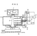
- Fig. 2 is a diagram showing another embodiment of the X-ray exposure apparatus according to the present invention, in which the same reference numerals as those in Fig. 1 designate the same or like components.
- an oxygen sensor 13 is provided outside the less-attenuation chamber 5.
- a plurality of pipes 30 with their respective ends inserted into the less attenuation chamber 5 at selected positions are connected at their other ends to the oxygen sensor 13.
- Valves 31 are interposed in the pipes 30 respectively, and oxygen in the less-attenuation chamber 5 is introduced by a vacuum pump 32 up to the oxygen sensor 13 to be detected there.
- the quantity of oxygen is detected for various portions within the less-attenuation chamber 5, so that there are such advantages that the quantity of oxygen is detected and controlled more accurately than the first embodiment and the maintenance such as calibration or the like for the oxygen sensor 13 can be easily performed.
- the former embodiment is superior to this embodiment in that the inside of the less-attenuation chamber 5 is not disturbed in the former.
- the oxygen sensor in Figs. 1 and 2 is replaced by a mass-analyzer, such as a mass spectrometer, it is possible to directly measure the relative quantity or ratio of helium gas.
- the density of gas may be measured by measuring the reflective index of light.
- a separate gas container having a known weight is provided separately from the less-attenuation chamber 5 and interconnected through a flexible pipe to the chamber so that the gas filled in the chamber 5 is introduced into the container and the gas density is determined by measuring a weight of the container including the introduced gas and calculating a net weight of the introduced gas.
Landscapes
- Physics & Mathematics (AREA)
- Engineering & Computer Science (AREA)
- General Physics & Mathematics (AREA)
- Health & Medical Sciences (AREA)
- Chemical & Material Sciences (AREA)
- Nanotechnology (AREA)
- Toxicology (AREA)
- Environmental & Geological Engineering (AREA)
- Epidemiology (AREA)
- Public Health (AREA)
- Mathematical Physics (AREA)
- Theoretical Computer Science (AREA)
- Life Sciences & Earth Sciences (AREA)
- Crystallography & Structural Chemistry (AREA)
- Atmospheric Sciences (AREA)
- Plasma & Fusion (AREA)
- Exposure Of Semiconductors, Excluding Electron Or Ion Beam Exposure (AREA)
- Exposure And Positioning Against Photoresist Photosensitive Materials (AREA)
Applications Claiming Priority (2)
| Application Number | Priority Date | Filing Date | Title |
|---|---|---|---|
| JP218383/84 | 1984-10-19 | ||
| JP59218383A JPS6197918A (ja) | 1984-10-19 | 1984-10-19 | X線露光装置 |
Publications (3)
| Publication Number | Publication Date |
|---|---|
| EP0178660A2 EP0178660A2 (en) | 1986-04-23 |
| EP0178660A3 EP0178660A3 (en) | 1988-04-20 |
| EP0178660B1 true EP0178660B1 (en) | 1990-09-12 |
Family
ID=16719037
Family Applications (1)
| Application Number | Title | Priority Date | Filing Date |
|---|---|---|---|
| EP85113171A Expired - Lifetime EP0178660B1 (en) | 1984-10-19 | 1985-10-17 | X-ray exposure apparatus |
Country Status (5)
| Country | Link |
|---|---|
| US (1) | US4825453A (Direct) |
| EP (1) | EP0178660B1 (Direct) |
| JP (1) | JPS6197918A (Direct) |
| KR (1) | KR900000437B1 (Direct) |
| DE (1) | DE3579664D1 (Direct) |
Families Citing this family (26)
| Publication number | Priority date | Publication date | Assignee | Title |
|---|---|---|---|---|
| US4648106A (en) * | 1984-11-21 | 1987-03-03 | Micronix Corporation | Gas control for X-ray lithographic system |
| JPS62291028A (ja) * | 1986-06-10 | 1987-12-17 | Nec Corp | X線露光装置 |
| DE68929356T2 (de) * | 1988-06-03 | 2002-05-23 | Canon K.K., Tokio/Tokyo | Verfahren und Vorrichtung zur Belichtung |
| EP0358521B1 (en) * | 1988-09-09 | 1995-06-07 | Canon Kabushiki Kaisha | An exposure apparatus |
| JPH0276212A (ja) * | 1988-09-13 | 1990-03-15 | Canon Inc | 多重露光方法 |
| JP2623127B2 (ja) * | 1988-10-05 | 1997-06-25 | キヤノン株式会社 | X線露光装置 |
| US5267292A (en) * | 1988-10-05 | 1993-11-30 | Canon Kabushiki Kaisha | X-ray exposure apparatus |
| JP2770960B2 (ja) * | 1988-10-06 | 1998-07-02 | キヤノン株式会社 | Sor−x線露光装置 |
| JPH02156625A (ja) * | 1988-12-09 | 1990-06-15 | Canon Inc | 直動案内装置 |
| EP0422814B1 (en) * | 1989-10-02 | 1999-03-17 | Canon Kabushiki Kaisha | Exposure apparatus |
| JP2860578B2 (ja) * | 1990-03-02 | 1999-02-24 | キヤノン株式会社 | 露光装置 |
| JP3184582B2 (ja) * | 1991-11-01 | 2001-07-09 | キヤノン株式会社 | X線露光装置およびx線露光方法 |
| US5512395A (en) * | 1993-04-30 | 1996-04-30 | Lsi Logic Corporation | Image masks for semiconductor lithography |
| US5572562A (en) * | 1993-04-30 | 1996-11-05 | Lsi Logic Corporation | Image mask substrate for X-ray semiconductor lithography |
| AU6853598A (en) * | 1997-04-18 | 1998-11-13 | Nikon Corporation | Aligner, exposure method using the aligner, and method of manufacture of circuitdevice |
| KR20010112265A (ko) * | 1999-02-12 | 2001-12-20 | 시마무라 테루오 | 노광방법 및 장치 |
| US6364386B1 (en) | 1999-10-27 | 2002-04-02 | Agilent Technologies, Inc. | Apparatus and method for handling an integrated circuit |
| US7508487B2 (en) * | 2000-06-01 | 2009-03-24 | Asml Netherlands B.V. | Lithographic apparatus, device manufacturing method, and device manufactured thereby |
| TWI226972B (en) * | 2000-06-01 | 2005-01-21 | Asml Netherlands Bv | Lithographic apparatus, device manufacturing method, and device manufactured thereby |
| US6576912B2 (en) * | 2001-01-03 | 2003-06-10 | Hugo M. Visser | Lithographic projection apparatus equipped with extreme ultraviolet window serving simultaneously as vacuum window |
| JP2002299221A (ja) * | 2001-04-02 | 2002-10-11 | Canon Inc | X線露光装置 |
| SG10201803122UA (en) * | 2003-04-11 | 2018-06-28 | Nikon Corp | Immersion lithography apparatus and device manufacturing method |
| TWI612556B (zh) * | 2003-05-23 | 2018-01-21 | 尼康股份有限公司 | 曝光裝置、曝光方法及元件製造方法 |
| KR20170016532A (ko) * | 2004-06-09 | 2017-02-13 | 가부시키가이샤 니콘 | 노광 장치 및 디바이스 제조 방법 |
| US8698998B2 (en) * | 2004-06-21 | 2014-04-15 | Nikon Corporation | Exposure apparatus, method for cleaning member thereof, maintenance method for exposure apparatus, maintenance device, and method for producing device |
| KR101342303B1 (ko) * | 2004-06-21 | 2013-12-16 | 가부시키가이샤 니콘 | 노광 장치 및 그 부재의 세정 방법, 노광 장치의 메인터넌스 방법, 메인터넌스 기기, 그리고 디바이스 제조 방법 |
Family Cites Families (10)
| Publication number | Priority date | Publication date | Assignee | Title |
|---|---|---|---|---|
| US2307754A (en) * | 1940-08-03 | 1943-01-12 | Allis Chalmers Mfg Co | Hydrogen-filled apparatus |
| US2804102A (en) * | 1954-08-09 | 1957-08-27 | Ralph D Cooksley | Automatic pressure container vacuumizing, filling and charging machine |
| US4119855A (en) * | 1977-07-08 | 1978-10-10 | Massachusetts Institute Of Technology | Non vacuum soft x-ray lithographic source |
| FR2475728A1 (fr) * | 1980-02-11 | 1981-08-14 | Cit Alcatel | Detecteur de fuites a helium |
| JPS57169242A (en) * | 1981-04-13 | 1982-10-18 | Hitachi Ltd | X-ray transferring device |
| US4349418A (en) * | 1981-07-28 | 1982-09-14 | Allied Corporation | Production of methylnaphthalenes and tar bases including indole |
| JPS58191433A (ja) * | 1982-05-04 | 1983-11-08 | Fujitsu Ltd | X線転写方法および装置 |
| JPS59101833A (ja) * | 1982-12-03 | 1984-06-12 | Hitachi Ltd | X線露光装置 |
| JPS6170721A (ja) * | 1984-09-14 | 1986-04-11 | Toshiba Corp | X線露光装置 |
| US4648106A (en) * | 1984-11-21 | 1987-03-03 | Micronix Corporation | Gas control for X-ray lithographic system |
-
1984
- 1984-10-19 JP JP59218383A patent/JPS6197918A/ja active Granted
-
1985
- 1985-10-16 KR KR1019850007603A patent/KR900000437B1/ko not_active Expired
- 1985-10-17 US US06/788,861 patent/US4825453A/en not_active Expired - Fee Related
- 1985-10-17 EP EP85113171A patent/EP0178660B1/en not_active Expired - Lifetime
- 1985-10-17 DE DE8585113171T patent/DE3579664D1/de not_active Expired - Lifetime
Also Published As
| Publication number | Publication date |
|---|---|
| JPH0564453B2 (Direct) | 1993-09-14 |
| DE3579664D1 (de) | 1990-10-18 |
| KR860003649A (ko) | 1986-05-28 |
| EP0178660A2 (en) | 1986-04-23 |
| EP0178660A3 (en) | 1988-04-20 |
| US4825453A (en) | 1989-04-25 |
| JPS6197918A (ja) | 1986-05-16 |
| KR900000437B1 (ko) | 1990-01-30 |
Similar Documents
| Publication | Publication Date | Title |
|---|---|---|
| EP0178660B1 (en) | X-ray exposure apparatus | |
| US6341006B1 (en) | Projection exposure apparatus | |
| EP0422814B1 (en) | Exposure apparatus | |
| EP0676672B1 (en) | Processing method and apparatus for a resist-coated substrate | |
| US6833903B2 (en) | Inert gas purge method and apparatus, exposure apparatus, reticle stocker, reticle inspection apparatus, reticle transfer box, and device manufacturing method | |
| US20030025889A1 (en) | Exposure apparatus and control method therefor, and device manufacturing method | |
| EP0540302B1 (en) | X-ray exposure apparatus and semiconductor-device manufacturing method | |
| JPH02106917A (ja) | 露光装置及び露光方法 | |
| JP3473649B2 (ja) | 投影露光装置 | |
| US4648106A (en) | Gas control for X-ray lithographic system | |
| EP0424181A2 (en) | X-ray exposure apparatus | |
| US5267292A (en) | X-ray exposure apparatus | |
| JP2003133622A (ja) | 紫外線レーザ装置 | |
| EP0363163B1 (en) | X-ray exposure apparatus | |
| JP3734043B2 (ja) | 露光装置 | |
| US6009144A (en) | X-ray system and X-ray exposure apparatus | |
| US20030090644A1 (en) | Mask and exposure apparatus | |
| JP3262138B2 (ja) | 露光方法及び装置 | |
| KR100433811B1 (ko) | 투영노광장치 | |
| Oertel et al. | Exposure instrumentation for the application of x‐ray lithography using synchrotron radiation | |
| JP2997090B2 (ja) | X線露光方法 | |
| JPH03108311A (ja) | X線露光装置 | |
| JP2004047518A (ja) | X線露光装置およびデバイスの製造方法 | |
| JPH0521320A (ja) | X線露光装置 | |
| JPS6258183A (ja) | 多チヤンネル検出器の相対感度較正装置 |
Legal Events
| Date | Code | Title | Description |
|---|---|---|---|
| PUAI | Public reference made under article 153(3) epc to a published international application that has entered the european phase |
Free format text: ORIGINAL CODE: 0009012 |
|
| AK | Designated contracting states |
Kind code of ref document: A2 Designated state(s): DE FR GB |
|
| PUAL | Search report despatched |
Free format text: ORIGINAL CODE: 0009013 |
|
| AK | Designated contracting states |
Kind code of ref document: A3 Designated state(s): DE FR GB |
|
| 17P | Request for examination filed |
Effective date: 19880421 |
|
| 17Q | First examination report despatched |
Effective date: 19890620 |
|
| GRAA | (expected) grant |
Free format text: ORIGINAL CODE: 0009210 |
|
| AK | Designated contracting states |
Kind code of ref document: B1 Designated state(s): DE FR GB |
|
| REF | Corresponds to: |
Ref document number: 3579664 Country of ref document: DE Date of ref document: 19901018 |
|
| ET | Fr: translation filed | ||
| PLBE | No opposition filed within time limit |
Free format text: ORIGINAL CODE: 0009261 |
|
| STAA | Information on the status of an ep patent application or granted ep patent |
Free format text: STATUS: NO OPPOSITION FILED WITHIN TIME LIMIT |
|
| 26N | No opposition filed | ||
| PGFP | Annual fee paid to national office [announced via postgrant information from national office to epo] |
Ref country code: GB Payment date: 19921007 Year of fee payment: 8 |
|
| PG25 | Lapsed in a contracting state [announced via postgrant information from national office to epo] |
Ref country code: GB Effective date: 19931017 |
|
| GBPC | Gb: european patent ceased through non-payment of renewal fee |
Effective date: 19931017 |
|
| PGFP | Annual fee paid to national office [announced via postgrant information from national office to epo] |
Ref country code: FR Payment date: 19960814 Year of fee payment: 12 |
|
| PG25 | Lapsed in a contracting state [announced via postgrant information from national office to epo] |
Ref country code: FR Free format text: THE PATENT HAS BEEN ANNULLED BY A DECISION OF A NATIONAL AUTHORITY Effective date: 19971031 |
|
| REG | Reference to a national code |
Ref country code: FR Ref legal event code: ST |
|
| PGFP | Annual fee paid to national office [announced via postgrant information from national office to epo] |
Ref country code: DE Payment date: 19981230 Year of fee payment: 14 |
|
| PG25 | Lapsed in a contracting state [announced via postgrant information from national office to epo] |
Ref country code: DE Free format text: LAPSE BECAUSE OF NON-PAYMENT OF DUE FEES Effective date: 20000801 |