EP0168351A1 - Générateur laser de motifs et procédé pour son emploi - Google Patents
Générateur laser de motifs et procédé pour son emploi Download PDFInfo
- Publication number
- EP0168351A1 EP0168351A1 EP85810307A EP85810307A EP0168351A1 EP 0168351 A1 EP0168351 A1 EP 0168351A1 EP 85810307 A EP85810307 A EP 85810307A EP 85810307 A EP85810307 A EP 85810307A EP 0168351 A1 EP0168351 A1 EP 0168351A1
- Authority
- EP
- European Patent Office
- Prior art keywords
- laser beam
- writing
- scanning laser
- detector
- scanning
- Prior art date
- Legal status (The legal status is an assumption and is not a legal conclusion. Google has not performed a legal analysis and makes no representation as to the accuracy of the status listed.)
- Granted
Links
Images


Classifications
-
- B—PERFORMING OPERATIONS; TRANSPORTING
- B23—MACHINE TOOLS; METAL-WORKING NOT OTHERWISE PROVIDED FOR
- B23K—SOLDERING OR UNSOLDERING; WELDING; CLADDING OR PLATING BY SOLDERING OR WELDING; CUTTING BY APPLYING HEAT LOCALLY, e.g. FLAME CUTTING; WORKING BY LASER BEAM
- B23K26/00—Working by laser beam, e.g. welding, cutting or boring
- B23K26/02—Positioning or observing the workpiece, e.g. with respect to the point of impact; Aligning, aiming or focusing the laser beam
- B23K26/04—Automatically aligning, aiming or focusing the laser beam, e.g. using the back-scattered light
- B23K26/046—Automatically focusing the laser beam
-
- B—PERFORMING OPERATIONS; TRANSPORTING
- B23—MACHINE TOOLS; METAL-WORKING NOT OTHERWISE PROVIDED FOR
- B23K—SOLDERING OR UNSOLDERING; WELDING; CLADDING OR PLATING BY SOLDERING OR WELDING; CUTTING BY APPLYING HEAT LOCALLY, e.g. FLAME CUTTING; WORKING BY LASER BEAM
- B23K26/00—Working by laser beam, e.g. welding, cutting or boring
- B23K26/02—Positioning or observing the workpiece, e.g. with respect to the point of impact; Aligning, aiming or focusing the laser beam
- B23K26/04—Automatically aligning, aiming or focusing the laser beam, e.g. using the back-scattered light
- B23K26/042—Automatically aligning the laser beam
-
- B—PERFORMING OPERATIONS; TRANSPORTING
- B23—MACHINE TOOLS; METAL-WORKING NOT OTHERWISE PROVIDED FOR
- B23K—SOLDERING OR UNSOLDERING; WELDING; CLADDING OR PLATING BY SOLDERING OR WELDING; CUTTING BY APPLYING HEAT LOCALLY, e.g. FLAME CUTTING; WORKING BY LASER BEAM
- B23K2101/00—Articles made by soldering, welding or cutting
- B23K2101/007—Marks, e.g. trade marks
Definitions
- the present invention relates to a method and a device for determining reference data for determining the position and for correcting mechanical movements when writing lines with a writing laser beam in a workpiece with a metallized, three-dimensional, integrated circuit.
- the aforementioned device is briefly referred to as a "laser pattern generator”.
- the European patent application (publication no. 0 088 045) describes a method for producing electrically conductive regions in integrated monolithic semiconductor arrangements and a semiconductor arrangement of high packing density produced thereafter.
- N and P structures are used, on which, depending on the intended use, specific contact surfaces have to be created to connect these structures.
- galvanically conductive areas with standardized cutouts which are arranged according to a predetermined grid, are produced on a silicon wafer, for example by an etching or application technique.
- the conductive layer made of aluminum is then removed directly or indirectly between these cutouts by means of an electron or electromagnetic beam.
- a laser beam is particularly suitable for this purpose, which can be easily positioned and controlled and is used to expose a photosensitive layer.
- the silicon wafers are continuously moved relative to the laser beam along the predetermined grid and the laser power is switched on and off with a modulator according to the desired ablation geometry.
- the grid spacing is on the order of 1-7 pm
- the width of the lines removed is 0.4-2 pm
- the processing speed is on the order of 1-2 hours per 4 "silicon wafer. This results in a movement speed of 30-100 cm / s and a position tolerance of 0.3-2.5 pm with a displacement length of 4 ". These values of the position tolerance cannot be achieved with mechanical displacement units.
- the insular conductive areas are then produced using a photo-etching technique. With this method, expensive application-specific photomasks can be dispensed with.
- a correspondingly manufactured semiconductor arrangement has on its conductive layer the cutouts arranged according to the predetermined grid, which represent end and / or corner points of insular conductive regions.
- the object of the present invention is to provide a method and a device of the type mentioned at the outset which precisely guide the writing laser beam with respect to the workpiece, even with three-dimensional structures, and enables both position determination or synchronization, as well as position correction or correction of the mechanically non-linear movement.
- This method and device are intended to create e.g. 2 pm wide dividing surfaces, i.e. of so-called lines with a speed of over 300 mm / s.
- the aforementioned object is achieved in that the metallized grid of the workpiece during the line-like working movements with the modulated i.e. by means of a modulator. attenuated or non-attenuated writing laser beam or a scanning laser beam brought on the same axis is scanned such that the reflected laser beam is received in at least one radiation detector and then evaluated, the evaluated signals being used to determine the position and to correct the relative movement of the workpiece and the writing laser beam.
- the advantage of the invention can be seen in the fact that the aforementioned method enables precise guidance of the mutual position of the workpiece and the writing laser beam, even in three-dimensional structures in which the scattered light occurs and could falsify the detection of the reference data, the writing laser beam being used both in the case of Write as can be used for scanning in the possibly weakened state.
- the laser beam or beams are sent vertically or with a deviation of up to + 10 ° on the machined surface of the integrated circuit of the workpiece. In the specified tolerance range, the writing laser beam or the scanning laser beam operates with sufficient reliability.
- the correction of the movement of the workpiece deviating from the line is carried out with a controllable beam deflector, e.g. carried out with a controllable deflecting mirror in front of the lens and / or with a controllable inclined plane plate after the lens and / or with a controllable displacement of the lens.
- a controllable beam deflector e.g. carried out with a controllable deflecting mirror in front of the lens and / or with a controllable inclined plane plate after the lens and / or with a controllable displacement of the lens.
- a modulation signal of the write laser beam directly controls the amplification factor of a signal amplifier, so that the same output signals are achieved even with different beam powers.
- the polarized write laser beam falls through a polarizing beam splitter as an analyzer of the electro-optical modulator beam switch onto the machined surface of the workpiece and the beam detector receives the same power in both states of the modulator beam switch.
- a scanning laser beam is used in addition to the writing laser beam, which is brought onto the same axis with a dichroic beam splitter and passes through the same beam path as the writing laser beam, thus compensating for unfavorable surface conditions of the integrated circuit of the workpiece for the wavelength of the writing laser beam and that The wavelength of the scanning laser beam is chosen differently from that of the writing laser beam.
- the diffuse scattered Light is measured with an additional detector and the ratio of the two signals is formed, thereby compensating for the different local surface properties of the integrated circuits of the workpiece, such as the reflection and scattering behavior of the metallized surface and the underlying materials.
- the writing laser beam (blue beam) and the scanning laser beam (red beam) are reflected in a laser beam collector with a writing laser beam splitter and a scanning laser beam mirror in a lens head and if a part of the writing laser beam is branched off with the writing laser beam splitter into a writing laser beam detector.
- both laser beams can be precisely aligned in the laser beam collector, which is additionally checked and controlled by the responsible write laser beam detector in the case of the writing laser beam.
- the metallized, three-dimensional, integrated circuit is covered with a photoresist layer which is exposed by the writing laser.
- the writing laser beam and the scanning laser beam in the laser beam collector are guided on the same axis to a scanning laser beam splitter of the lens head, from which the scanning laser beam and the writing laser beam are guided through the lens onto the workpiece.
- Part of the reflected scanning laser beam is reflected by the scanning laser beam splitter into a turret.
- the laser light signals detected in detectors and / or from the objective head and / or from the turret head are evaluated and the functional position is thus detected or achieved.
- This method can work automatically with sufficient accuracy using known electronic means.
- the device for carrying out the method according to claim 1 contains, according to claim 11, a writing laser device with a downstream modulator, an expander and an objective, and a beam splitter of the reflected light is assigned to a detector for evaluation.
- the beam splitter is a polarizing beam splitter which is provided as an analyzer of the electro-optical modulator.
- the laser writing device additionally contains a scanning laser device with a wavelength different from the writing laser device and that the device with a dichroic beam splitter for superimposing the scanning laser beam on the axis of the writing laser beam and for subsequently separating the scanning laser beam onto a detector is provided.
- the use of the dichroic beam splitter enables simple evaluation when using two lasers with different wavelengths.
- a control device for achieving the correct mutual position of the integrated circuit and the laser radiation contains a control circuit which consists of an operational amplifier with a downstream high-voltage amplifier and there is at least one piezo element.
- the at least one piezo element is particularly suitable for mechanically very fine and fast control of the moving parts.
- the objective head forms a common optical module with the turret head, the connecting part of which is only the scanning laser beam splitter.
- This solution is particularly expedient because there is no deflection mirror between the lens head and the turret head which influences the scanning surface of the detector and thus its speed.
- the laser beam collector is provided with a writing laser beam detector. This construction makes it possible to correct the direction and possibly also the width of the writing laser beam directly behind the writing laser beam source and to detect any inaccuracies.
- the turret head is provided with at least two of the three units: scanning laser beam detector, shear interferometer eyepiece and microscope eyepiece with crosshairs.
- scanning laser beam detector shear interferometer eyepiece
- microscope eyepiece with crosshairs.
- the writing laser beam source and / or the scanning laser beam source are each provided with at least one pinhole within the expander. This measure ensures sufficient image information-free laser beams, such as are expedient in the novel methods.
- the pinhole is also referred to as a "pinhole”.
- the microscope eyepiece of the objective head is expediently provided with a write laser blocking filter. This solution prevents the human eye from being damaged if the radiation power is too high.
- a detector is arranged behind the scanning laser beam splitter in the direction of the writing and scanning laser beams guided on the same axis. This further detector can control the direction of the common beam path of the scanning and writing laser beams.
- At least one detector consists of several fields. This solution not only signals a possible deviation from the desired direction but also the direction in which this deviation takes place. This facilitates the evaluation of a possible deviation and its automatic correction.
- the writing laser beam source A contains a writing laser device 1, behind which there is a laser beam switch 2 for switching off the writing laser beam 7 when the device is open.
- a pinhole 2 ' is arranged in an expander 4 of the writing laser device 1. Between these components there is a modulator 3 in the optical axis. Lenses of the expander 4 are denoted by the number 4 'and the entire writing laser beam source A is mounted in a housing 5. The modulator 3 and the expander 4 are held in the housing 5 with adjustable fastening elements 6.
- the entire housing 5 is also provided with adjustable fastening elements 6, which make it possible to correctly arrange the optical axis of this writing laser beam source A.
- the writing laser beam is designated by reference number 7.
- the scanning laser beam source B is mounted in a housing 8. It contains a scanning laser device 9, from which a scanning laser beam 9 'is directed into the expander 10 of the scanning laser beam source B. In addition to the already mentioned lenses 4 ', this expander 10 also contains a pinhole 11.
- the scanning laser beam source B also contains other elements which have already been mentioned in the description of the writing laser beam source A.
- a scanning laser beam 9 ' is guided into the expander 10 from the scanning laser device 9.
- the components of the scanning laser beam source are stored in a housing 8 which, like the housing 5 of the writing laser beam source A, is brought into the correct position with adjustable fastening elements 6 can be.
- a laser beam collector C In the direction of the optical axes of the writing laser beam 7 and the scanning laser beam 9 'there is a laser beam collector C.
- These elements are adjustable in the housing 12 by means of adjusting elements 16.
- To the left of the write laser beam splitter 13 is a write laser beam detector 15, which controls the correct starting position of the write laser beam 7.
- the reflected writing laser beam 7 and the reflected scanning laser beam 9 1 connect on the same axis 17, which then leads directly to FIG. 1b.
- 1b has a vertical optical axis.
- the common beam path 17 first falls on a scanning laser beam splitter 18. From this, the major part of the radiation goes into the lens 19 of the lens head D and further onto the workpiece D. In the direction of the writing and scanning laser beams 17 guided on the same axis is located behind the Scanning laser beam splitter 18 a detector 18 '. The task of this detector 18 'is to monitor the correct beam path 17.
- the lens 19 has setting elements 20, some of which are provided with a piezoelectric drive 21.
- a revolver head E is rotatably arranged directly above the objective head D, this objective head D and the revolver head E forming a functional unit, an optical module F.
- the objective head E essentially contains a revolver holder 22, on which, in this example, a scanning laser beam detector 23, a shear interferometer eyepiece 24 (shearing interferometer) and a microscope eyepiece 25 with crosshairs are rotatably located. For safety reasons, this microscope eyepiece 25 is provided with a write laser blocking filter 25 '.
- turret 1b shows the revolver head E in a developed, i.e. linear form. The correct circular shape will be seen later in FIG. 6.
- FIG. 2 shows a front view of the laser beam collector C.
- the write laser beam splitter 13 already described is gimbally suspended in a holder 26.
- the scanning laser beam mirror 14, which has also already been mentioned, is arranged in a similar manner in a holder 27.
- several support elements 28 of the laser beam collector C are not important for the functioning of the method and the device, it goes without saying that they are made sufficiently solid, which incidentally also applies to guide plates 28 ′ of the holders 26, 27 and a connecting body 30. Set screws 29 are used for the adjustment of the holders 26, 27.
- the solid connecting body 30 connects the support elements 28 to a work table 31.
- the already mentioned writing laser beam detector 15 is also attached to a support element 28 in the left part of FIG. 2.
- FIG. 3 illustrates a top view of the construction according to FIG. 2. The components have already been described.
- the set screws 29 'and guide plates 28' are also shown. These set screws 29 together with the set screws 29 'enable the elements 13, 14 to be set correctly.
- FIG 4 shows a partial vertical section through the optics module F, which consists of the objective head D in the lower part and the turret head E in the upper part.
- the components of the lens head D are essentially held by four rods 32 which are guided parallel to the optical axis through the entire lens head D and are mounted in rod holders 33.
- rod holders 33 In the lower part of the lens head D is the mutual position of two Rod holders 33 fixed by means of two leaf springs 34.
- the scanning laser beam splitter 18 is mounted in a holder 35.
- the scanning and scanning laser beams which are guided on the same axis and which are designated in this common beam path with the reference number 17, come from the left onto this scanning laser beam splitter 18.
- a lens holding ring 36 also serves to hold the lens 19.
- the piezoelectric drive 21 is provided for movements perpendicular to the optical axis.
- the rod holder 33 and other fastening elements are held together with screws 37, only a few of which are shown because they do not relate to the inventive idea and screw connections are of course known per se.
- a turret turntable 38 With the upper part of the lens head D, a turret turntable 38 is rotatably connected.
- three independent elements are stored in the turret head E. Above all one should mention a prism 40, with which one can bring the horizontal optical axis in the vertical direction.
- the shear interferometer contains an eyepiece 24 with a focusing screen and a flat plate 39.
- the turret head E further contains the microscope eyepiece 25 with a cross hair and the scanning laser beam detector 23.
- a write laser blocking filter 25 'and a tube lens 41 are mounted in the vertical optical axis under the prism 40.
- FIG. 5 shows the section V-V from FIG. 4. It is therefore the section through the lens head D, where the attachment of this lens head D is also clearly visible.
- the multi-part carrier 43 is shown, which contains a thick plate and serves to receive the fastening screw 44 of the turret head E.
- FIG. 6 shows a simplified top view of the turret E.
- This drawing illustrates the scanning laser beam detector 23 with a locking pin 46 as well as the shear interferometer eyepiece 24 with a plane plate 39 and the microscope eyepiece 25. All of these three parts are rotatably fastened with a holder 45 so that the desired apparatus can be inserted into the optical system as desired Axis of the lens head D can bring.
- the carrier 43 on which the turret head E is fastened is also visible in this drawing.
- FIG. 7 shows in simplified form an example of a detector, in this case the scanning laser beam detector 23, which is composed of several fields 47. If the function is correct, the middle field is irradiated; if there is a deviation from this desired position, one or more secondary fields are recorded. Because these fields 47 can be evaluated individually, this gives the information in which direction the deviation from the correct position extends.
- a naturally air-cooled helium-cadmium laser system (brand Liconix, Sunnyvale, CA 94086, USA) was used as the writing laser device 1.
- This laser device consists of a current-controlled high-voltage power supply Liconix, model 4200 PS, with cold and warm start, with time program and ignition control, as well as a laser device model 4110B.
- the main features of the writing laser device 1 are as follows: light wavelength 442 nm, light output is 10 mW (continuous light), the intensity is normally distributed over the beam diameter, polarization direction is horizontal + -5%, beam diameter 1.1 mm.
- the scanning laser device 9 is a naturally air-cooled Melles Griot, (ILEE AG, CH-Schlieren) helium-neon laser system, consisting of laser device, model 05-LHP-111 and model 05-LPN-340 supply device (1800 V, 6.5 mA ).
- the light wavelength is 633 nm
- light output is 1 mW
- deviation of the beam axis after the cold start is ⁇ 200 pRad
- after 15 minutes of operation 30 uRad after 15 minutes of operation 30 uRad.
- the beam divergence is ⁇ 1.3 mRad
- control deviation of the light output is ⁇ + -5%.
- the modulator 3 is a naturally air-cooled, electrically controlled Coherent blue laser light interrupter system (Coherent Associates, Danbury, Conn. 06810, USA), consisting of the control unit model 31 and the modulator model 3010.
- the modulator tube contains a break-sensitive, Potassium dihydrogen phosphate crystal embedded in liquid with the same refractive index with two control electrodes and a photodiode light meter attached to the output.
- the crystal acts as a polarization filter, the directional angle of which can be rotated with a voltage of approx. 600 V over 90 degrees.
- the expander 4 consists of two converging lenses and a pinhole, which is also called “pinhole”, with a diameter of 10 pm, in the common focus of the converging lenses.
- the expander enlarges the diameter and reduces the divergence of the laser beam in the expansion ratio, that is the ratio of the focal point distances, and transmits the image of the light spot in the pinhole in the output beam, i.e. removes e.g. dark spots of the incoming laser beam created due to dust and makes the direction of the output beam independent of the direction of the input beam.
- a dichroic divider which consists of a plane-parallel glass plate with a dielectric metal layer evaporated on one side. This lets the light of the certain wavelength, i.e. the one color that arrives in the direction of passage, in the same direction, displaces the radiation exit point depending on the refractive index of the glass for the specific wavelength, depending on the thickness of the glass.
- the piezoelectric drive 21 known per se in this example consists of a Burley, model PZ70, 1000 V power supply and a Burley, model PZ40 piezotranslator.
- the piezocrystal stack expands approximately proportionally with the applied voltage and thereby shifts the objective 19 in the horizontal axis.
- a microscope consists of the objective 19 and the microscope eyepiece 25.
- the objective 19 has a converging lens system with or without a standard cover glass on the working side, focuses the concentrically and parallel blue and red laser beam to the smallest possible focal spot in the working distance, guides an enlarged aerial view of the concentric to the focal spot lying green illuminated image field, which can be viewed with the microscope eyepiece 25. It converts the mechanical displacement by the piezoelectric drive 21 into a displacement of the center of the image and focal spot.
- the microscope eyepiece 25 is designed as a converging lens system with the function of a magnifying glass and derives an enlarged, visible image from the aerial image of the objective 19.
- the shear interferometer consists of a mirror that can be inserted into the beam path, a plane-parallel glass plate 39, and an eyepiece 24, and forms a shear interferometer for measuring the deviation of the distance of the reflective aluminum surface from the focusing plane of the Lens 19.
- the detectors 15, 18 1 and 23 expediently each consist of a central, inner insensitive and an outer more sensitive arrangement of silicon photodiodes. They use the laser beam reflected from the workpiece or obtained in another way to determine whether the responsible laser beam is in the correct position or is moving in a certain direction away from this position.
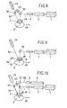
- Figures 8 to 13 show a schematic representation of some possible variants of the subject matter of the invention.
- FIG. 8 shows a simplified functional diagram of the device according to the invention with a single laser device 1.
- a workpiece 9 is made from a silicon plate and provided with a metallic grid, which is only shown in the next drawings.
- An arrow 48 shows the direction of movement of the workpiece G.
- Numeral 49 denotes a writing laser beam which falls from a writing laser 1 through a modulator 3 and an expander 4 onto a deflection mirror 50.
- This writing laser beam 49 corresponds to the writing laser beam 7, but is drawn in dashed lines for reasons of clarity.
- the write laser beam 49 is then guided through the lens head D with a lens onto the machined workpiece G.
- the light 51 reflected by the workpiece G falls on a beam splitter 52. A part of the light is guided by this into a detector 53 and part of the reflected light passes through the beam splitter 52 into a microscope eyepiece 25.
- FIG. 9 essentially corresponds to FIG. 8 with the difference that a polarizing beam splitter 54 is arranged in the objective D, which directs a polarization direction of the reflected light into the detector 53.
- FIG. 10 shows a solution where a scanning laser beam 55 is also used.
- This scanning laser beam 55 corresponds to the Taslaserstrahl 9 'in the first example, but is drawn in dotted lines for the sake of clarity, so that the function of the laser beams can be seen from the drawings.
- This solution is useful when the nature of the surface of the workpiece G needs two different wavelengths.
- the scanning laser beam 55 is generated in a scanning laser device 9 and further guided through an expander 10 onto a deflection mirror 50. From this deflecting mirror 50, the scanning laser beam 55 reflects through the dichroic beam splitter 56 and through the lens head D together with the writing laser beam 49 onto the surface of the workpiece G. Both laser beams hit the workpiece G in the same line and also in the same line they contact the beam splitter 52 The scanning laser beam 55 is reflected by this beam splitter 52 into the detector 53. The reflected writing laser beam 51 enters the microscope eyepiece 25.
- the beam splitter 52 is arranged in front of the objective D and the reflected writing laser beam 49 is then guided into the detector 53 and into the microscope eyepiece 25 with the aid of a further beam splitter 52.
- a polarizing beam splitter 54 is arranged directly in the lens head D, which guides a polarization direction of the reflected light 51 into the beam detector 53, the microscope eyepiece 25 receiving the reflected light directly from the beam splitter 52.
- both the writing laser beam 49 and the scanning laser beam 55 are used again; they are guided perpendicular to the workpiece G.
- a beam splitter 52 is arranged in the common path of the two laser beams and, as in FIG. 12, simultaneously a part of the light conducts into the detector 53 and some of the light into the microscope eyepiece 25.
- FIG. 14 shows a variant in which both the reflected light 51 and the diffuse light 58 are detected.
- a detector 57 is used for the detection of the reflected light 51 and a detector 60 for the detection of the diffuse light 58.
- the detector 60 of the diffuse light 58 is arranged around the laser beam 49.
- 61 denotes the surfaces with an integrated circuit, a metallized grid 62 serving as a reference structure.
- a laser spot 63a lies directly on the metallized grid 62, the second laser spot 63b partially on the metallized grid 62 and the third laser spot 63c directly on the integrated circuit 61.
- FIGS. 16a to 16c The corresponding reflected intensity distributions are shown in FIGS. 16a to 16c.
- the ideal course of the intensity distribution is shown in dashed lines in FIG. 16a, the actual course with the full line 64a. This is similar in FIG. 16b, where a deviation of curve 64b from the ideal state is shown. 17c shows the ideal state, which means that the actual course of the intensity distribution 64c is identical to the ideal course.
- the metallized grid 62 serves as a reference structure in the device according to the invention.
- the distance between two grid strips is, for example, 7 pm and their width is 5 pm (FIG. 15).
- the writing laser device 1 is, for example, an argon ion laser of 1 to 5 mW power at a wavelength of 458 nm (for example Spectra Physics, Mountain View, California, Mod. 162A.07; American Laser Corp., Salt Lake City, Utah, Mod. 60C), or a He-Cd laser from 7 to 40 mW Lei power at 442 nm, or 1 to 10 mW at 325 nm (e.g. Liconix, Sunnyvale, California, Mod. 4200 N or Mod. 4200 NB).
- the switching of the continuous laser power is also carried out with an electro-optical modulator beam switch 3 (e.g. Coherent Inc., Palo Alto, California, Modulator Div. Mod. 3010) or an acousto-optical modulator beam switch (e.g. Coherent Modulator Div. Mod. 304D).
- the required switching time results from the writing speed and the local resolution and is e.g. 2 us.
- the subsequent beam expander 4 increases the beam diameter e.g. ten times.
- the horizontal writing beam 49 is deflected in the vertical direction with the deflecting mirror 50.
- the objective 19 has a focal length of 18 mm and a diameter of 10 mm.
- the resulting spot size is about 2 ⁇ m and the depth of field is about 13 ⁇ m.
- the deflecting mirror 50 can be arranged to be controllable or adjustable.
- the scanning laser device 9 is a He-Ne laser with a power of 1 mW and a beam diameter of 0.65 mm. This is enlarged 4-fold with an expander 10 and superimposed on the writing laser beam 49 with an adjustable deflecting mirror 50.
- FIG. 8 shows separate scanning and writing laser beams 49, 55, which are, however, brought onto the same axis with the help of of dichroic mirror 56.
- This mirror has the advantage that it has 100% transmission for one wavelength and 100% reflection for another wavelength.
- This solution also makes it possible to focus both laser beams 49, 55 with the same objective.
- the variants according to FIGS. 11 to 13 are particularly suitable for workpieces with a high relief.
Priority Applications (1)
| Application Number | Priority Date | Filing Date | Title |
|---|---|---|---|
| AT85810307T ATE37153T1 (de) | 1984-07-10 | 1985-07-04 | Laser-pattern-generator und verfahren zu dessen betrieb. |
Applications Claiming Priority (4)
| Application Number | Priority Date | Filing Date | Title |
|---|---|---|---|
| CH333784 | 1984-07-10 | ||
| CH3337/84 | 1984-07-10 | ||
| CH2174/85A CH667830A5 (de) | 1985-05-22 | 1985-05-22 | Verfahren und vorrichtung zur positionsbestimmung und zur korrektur von mechanischen bewegungen bei einem laser-pattern-generator. |
| CH2174/85 | 1985-05-22 |
Publications (2)
| Publication Number | Publication Date |
|---|---|
| EP0168351A1 true EP0168351A1 (fr) | 1986-01-15 |
| EP0168351B1 EP0168351B1 (fr) | 1988-09-14 |
Family
ID=25689713
Family Applications (1)
| Application Number | Title | Priority Date | Filing Date |
|---|---|---|---|
| EP85810307A Expired EP0168351B1 (fr) | 1984-07-10 | 1985-07-04 | Générateur laser de motifs et procédé pour son emploi |
Country Status (3)
| Country | Link |
|---|---|
| US (1) | US4695698A (fr) |
| EP (1) | EP0168351B1 (fr) |
| DE (1) | DE3564914D1 (fr) |
Cited By (8)
| Publication number | Priority date | Publication date | Assignee | Title |
|---|---|---|---|---|
| EP0252268A2 (fr) * | 1986-07-11 | 1988-01-13 | BIAS Forschungs- und Entwicklungslabor für angewandte Strahltechnik | Procédé pour la surveillance de source d'énergie d'usinage, en particulier d'un laser, et optique d'usinage pour la réalisation de celui-ci |
| EP0253764A1 (fr) * | 1986-06-25 | 1988-01-20 | Lasarray Holding Ag | Méthode et dispositif pour augmenter la sécurité d'un système relatif à un procédé d'écriture par laser |
| EP0262088A1 (fr) * | 1986-09-22 | 1988-03-30 | Lasarray Holding AG | Arrangement pour le positionnement et la synchronisation d'un rayon laser d'écriture |
| EP0299702A1 (fr) * | 1987-07-15 | 1989-01-18 | Westinghouse Electric Corporation | Système de forage avec laser controllé à l'égard de la profondeur |
| FR2657219A1 (fr) * | 1990-01-11 | 1991-07-19 | Gim Ind Sa | Procede de fabrication de circuits imprimes souples, circuit imprime fabrique par ce procede, et dispositif pour la mise en óoeuvre de ce procede. |
| EP0495647A1 (fr) * | 1991-01-17 | 1992-07-22 | United Distillers Plc | Marquage dynamique au laser |
| US6791592B2 (en) | 2000-04-18 | 2004-09-14 | Laserink | Printing a code on a product |
| US10583668B2 (en) | 2018-08-07 | 2020-03-10 | Markem-Imaje Corporation | Symbol grouping and striping for wide field matrix laser marking |
Families Citing this family (20)
| Publication number | Priority date | Publication date | Assignee | Title |
|---|---|---|---|---|
| US4969169A (en) * | 1986-04-15 | 1990-11-06 | Hampshire Instruments, Inc. | X-ray lithography system |
| US5379059A (en) * | 1988-10-03 | 1995-01-03 | Cirrus Technology Inc. | Adjustment mechanism for equipment converting digital data into a light image |
| US4933687A (en) * | 1988-10-03 | 1990-06-12 | Cirrus Technology Inc. | Laser-actuated digital imaging system |
| JP2696364B2 (ja) * | 1988-12-01 | 1998-01-14 | 旭光学工業株式会社 | 走査式光学装置のモニター機構 |
| US5294943A (en) * | 1991-10-31 | 1994-03-15 | Eastman Kodak Company | Method and apparatus for alignment of scan line optics with target medium |
| US5643476A (en) * | 1994-09-21 | 1997-07-01 | University Of Southern California | Laser system for removal of graffiti |
| US6331691B1 (en) * | 1999-09-20 | 2001-12-18 | Automated Laser Corporation | Precision guiding apparatus for laser marking system |
| US7046267B2 (en) | 2003-12-19 | 2006-05-16 | Markem Corporation | Striping and clipping correction |
| US7800014B2 (en) | 2004-01-09 | 2010-09-21 | General Lasertronics Corporation | Color sensing for laser decoating |
| US7633033B2 (en) | 2004-01-09 | 2009-12-15 | General Lasertronics Corporation | Color sensing for laser decoating |
| US20060021977A1 (en) * | 2004-07-30 | 2006-02-02 | Menegus Harry E | Process and apparatus for scoring a brittle material incorporating moving optical assembly |
| US7394479B2 (en) | 2005-03-02 | 2008-07-01 | Marken Corporation | Pulsed laser printing |
| US8536483B2 (en) * | 2007-03-22 | 2013-09-17 | General Lasertronics Corporation | Methods for stripping and modifying surfaces with laser-induced ablation |
| KR100887653B1 (ko) | 2007-06-19 | 2009-03-11 | 연세대학교 산학협력단 | 계측 유닛을 구비한 스캔 타입 레이저 가공 장치 |
| WO2009005840A1 (fr) * | 2007-07-05 | 2009-01-08 | General Lasertronics Corporation | Adaptateurs d'ouverture destinés à un organe terminal effecteur pour l'élimination de revêtement à base de laser |
| US8804102B2 (en) * | 2010-05-19 | 2014-08-12 | Materials Solutions | Laser scan speed calibration |
| GB201008334D0 (en) * | 2010-05-19 | 2010-07-07 | Materials Solutions | Laser scan speed calibration |
| US10112257B1 (en) | 2010-07-09 | 2018-10-30 | General Lasertronics Corporation | Coating ablating apparatus with coating removal detection |
| US9895771B2 (en) | 2012-02-28 | 2018-02-20 | General Lasertronics Corporation | Laser ablation for the environmentally beneficial removal of surface coatings |
| US10086597B2 (en) | 2014-01-21 | 2018-10-02 | General Lasertronics Corporation | Laser film debonding method |
Citations (1)
| Publication number | Priority date | Publication date | Assignee | Title |
|---|---|---|---|---|
| US3626141A (en) * | 1970-04-30 | 1971-12-07 | Quantronix Corp | Laser scribing apparatus |
Family Cites Families (1)
| Publication number | Priority date | Publication date | Assignee | Title |
|---|---|---|---|---|
| US4002829A (en) * | 1974-08-29 | 1977-01-11 | W. R. Grace & Co. | Autosynchronous optical scanning and recording laser system with fiber optic light detection |
-
1985
- 1985-07-02 US US06/751,258 patent/US4695698A/en not_active Expired - Fee Related
- 1985-07-04 DE DE8585810307T patent/DE3564914D1/de not_active Expired
- 1985-07-04 EP EP85810307A patent/EP0168351B1/fr not_active Expired
Patent Citations (1)
| Publication number | Priority date | Publication date | Assignee | Title |
|---|---|---|---|---|
| US3626141A (en) * | 1970-04-30 | 1971-12-07 | Quantronix Corp | Laser scribing apparatus |
Non-Patent Citations (3)
| Title |
|---|
| CONFERENCE ON LASER AND ELECTROOPTICAL SYSTEMS, 7.-9. Februar 1978, Seiten 90-92, Digest of Technical Papers, Optical Society of America, IEEE, Washington, US; M.P. FEDER et al.: "Nitrogen-pumped dye laser tool for fabricating LSI connections" * |
| PATENTS ABSTRACTS OF JAPAN, Band 6, Nr. 267 (M-182)[1145], 25. Dezember 1982, Seite 102 M 182; & JP - A - 57 159 286 (MITSUBISHI DENKI K.K.) 01-10-1982 * |
| PATENTS ABSTRACTS OF JAPAN, Band 7, Nr. 250 (M-254)[1395], 8. November 1983, Seite 118 M 254; & JP - A - 58 135 788 (HITACHI SEISAKUSHO K.K.) 12-08-1983 * |
Cited By (15)
| Publication number | Priority date | Publication date | Assignee | Title |
|---|---|---|---|---|
| EP0253764A1 (fr) * | 1986-06-25 | 1988-01-20 | Lasarray Holding Ag | Méthode et dispositif pour augmenter la sécurité d'un système relatif à un procédé d'écriture par laser |
| US4871896A (en) * | 1986-06-25 | 1989-10-03 | Lasarray Holding Ag | Process and device to enhance system performance accuracy in a laser writing process |
| EP0252268A2 (fr) * | 1986-07-11 | 1988-01-13 | BIAS Forschungs- und Entwicklungslabor für angewandte Strahltechnik | Procédé pour la surveillance de source d'énergie d'usinage, en particulier d'un laser, et optique d'usinage pour la réalisation de celui-ci |
| EP0252268A3 (en) * | 1986-07-11 | 1989-02-01 | Bias Forschungs- Und Entwicklungslabor Fur Angewandte Strahltechnik | Process for monitoring the machining energy source, particularly with a laser, and machining optics for its implementation |
| EP0262088A1 (fr) * | 1986-09-22 | 1988-03-30 | Lasarray Holding AG | Arrangement pour le positionnement et la synchronisation d'un rayon laser d'écriture |
| EP0299702A1 (fr) * | 1987-07-15 | 1989-01-18 | Westinghouse Electric Corporation | Système de forage avec laser controllé à l'égard de la profondeur |
| FR2657219A1 (fr) * | 1990-01-11 | 1991-07-19 | Gim Ind Sa | Procede de fabrication de circuits imprimes souples, circuit imprime fabrique par ce procede, et dispositif pour la mise en óoeuvre de ce procede. |
| WO1991011090A1 (fr) * | 1990-01-11 | 1991-07-25 | Gim Industrie S.A. | Procede de fabrication de circuits imprimes souples, circuit imprime fabrique par ce procede, et dispositif pour la mise en ×uvre de ce procede |
| US5278385A (en) * | 1990-01-11 | 1994-01-11 | Nicolitch S.A. | Method of producing flexible printed circuits, printed circuit produced by this method and device for carrying out this method |
| EP0495647A1 (fr) * | 1991-01-17 | 1992-07-22 | United Distillers Plc | Marquage dynamique au laser |
| WO1992012820A1 (fr) * | 1991-01-17 | 1992-08-06 | United Distillers Plc | Marquage au laser dynamique |
| US5653900A (en) * | 1991-01-17 | 1997-08-05 | United Distillers Plc | Dynamic laser marking |
| US6791592B2 (en) | 2000-04-18 | 2004-09-14 | Laserink | Printing a code on a product |
| US6829000B2 (en) | 2000-04-18 | 2004-12-07 | Laserink | Printing a code on a product |
| US10583668B2 (en) | 2018-08-07 | 2020-03-10 | Markem-Imaje Corporation | Symbol grouping and striping for wide field matrix laser marking |
Also Published As
| Publication number | Publication date |
|---|---|
| US4695698A (en) | 1987-09-22 |
| DE3564914D1 (en) | 1988-10-20 |
| EP0168351B1 (fr) | 1988-09-14 |
Similar Documents
| Publication | Publication Date | Title |
|---|---|---|
| EP0168351B1 (fr) | Générateur laser de motifs et procédé pour son emploi | |
| EP3049755B1 (fr) | Procédé de mesure de la profondeur de pénétration d'un faisceau laser dans une pièce à usiner et dispositif d'usinage laser | |
| DE102015001421B4 (de) | Vorrichtung und Verfahren zur Strahldiagnose an Laserbearbeitungs-Optiken (PRl-2015-001) | |
| EP1097022B1 (fr) | Procede et dispositif pour etalonner une machine d'usinage de pieces par laser | |
| DE2256736C3 (de) | Meßanordnung zur automatischen Prüfung der Oberflächenbeschaffenheit und Ebenheit einer Werkstückoberfläche | |
| EP1656234B1 (fr) | Tete de balayage faisant partie d'un dispositif de forage et de decoupe laser | |
| DE102009059245B4 (de) | Verfahren und Vorrichtung zur Erfassung und Justierung des Fokus eines Laserstrahls bei der Laserbearbeitung von Werkstücken | |
| EP3583390B1 (fr) | Procédé et dispositif de détection d'une position focale d'un faisceau laser | |
| DE112017001222T5 (de) | Laserlicht-Bestrahlungsvorrichtung und Laserlicht-Bestrahlungsverfahren | |
| DE3021622A1 (de) | Optisches abbildungssystem mit einem optoelektronischen detektionssystem zur bestimmung einer abweichung zwischen der bildflaeche des abbildungssystems und einer zweiten flaeche, auf der abgebildet wird | |
| DE3439017A1 (de) | Augenchirurgisches lasergeraet | |
| DE3538062C2 (de) | Positionserfassungsgerät | |
| DE2333281C3 (de) | Verfahren zur Ermittlung der Fokussierung eines auf ein Objekt ausgesandten kohärenten Lichtstrahls | |
| DE3806209A1 (de) | Strukturdefekt-erfassungssystem | |
| EP4041487A1 (fr) | Dispositif d'ajustement pour un système optique d'usinage par faisceau de bessel et procédé correspondant | |
| DE112017000543T5 (de) | Laserstrahl-bestrahlungsvorrichtung | |
| DE2034341B2 (de) | Vorrichtung zur Materialbearbeitung mittels Laserstrahlen | |
| DE4426069A1 (de) | Laser-Zeicheneinrichtung | |
| DE102019201280A1 (de) | Anordnung und Verfahren zum Formen eines Laserstrahls | |
| DE3940694A1 (de) | Strahlengang-einstellvorrichtung | |
| DE2206520A1 (de) | Verfahren zur eliminierung eines systematischen messfehlers bei optischen anemometern | |
| EP0262088B1 (fr) | Arrangement pour le positionnement et la synchronisation d'un rayon laser d'écriture | |
| DE3807659C2 (fr) | ||
| EP0128993B1 (fr) | Procédé de détermination de références pour la correction de mouvements mécaniques lors de l'écriture de lignes dans une trame métallisée à l'aide d'un laser ainsi que l'appareil pour réaliser ce procédé | |
| DE202009014893U1 (de) | Vorrichtung zur Erfassung und Justierung des Fokus eines Laserstrahls bei der Laserbearbeitung von Werkstücken |
Legal Events
| Date | Code | Title | Description |
|---|---|---|---|
| PUAI | Public reference made under article 153(3) epc to a published international application that has entered the european phase |
Free format text: ORIGINAL CODE: 0009012 |
|
| AK | Designated contracting states |
Designated state(s): AT BE CH DE FR GB IT LI LU NL SE |
|
| 17P | Request for examination filed |
Effective date: 19860219 |
|
| RAP1 | Party data changed (applicant data changed or rights of an application transferred) |
Owner name: LASARRAY HOLDING AG |
|
| 17Q | First examination report despatched |
Effective date: 19861203 |
|
| D17Q | First examination report despatched (deleted) | ||
| GRAA | (expected) grant |
Free format text: ORIGINAL CODE: 0009210 |
|
| ITF | It: translation for a ep patent filed |
Owner name: ING. ZINI MARANESI & C. S.R.L. |
|
| AK | Designated contracting states |
Kind code of ref document: B1 Designated state(s): AT BE CH DE FR GB IT LI LU NL SE |
|
| REF | Corresponds to: |
Ref document number: 37153 Country of ref document: AT Date of ref document: 19880915 Kind code of ref document: T |
|
| GBT | Gb: translation of ep patent filed (gb section 77(6)(a)/1977) | ||
| REF | Corresponds to: |
Ref document number: 3564914 Country of ref document: DE Date of ref document: 19881020 |
|
| ET | Fr: translation filed | ||
| PLBE | No opposition filed within time limit |
Free format text: ORIGINAL CODE: 0009261 |
|
| STAA | Information on the status of an ep patent application or granted ep patent |
Free format text: STATUS: NO OPPOSITION FILED WITHIN TIME LIMIT |
|
| 26N | No opposition filed | ||
| PGFP | Annual fee paid to national office [announced via postgrant information from national office to epo] |
Ref country code: SE Payment date: 19910626 Year of fee payment: 7 Ref country code: LU Payment date: 19910626 Year of fee payment: 7 |
|
| PGFP | Annual fee paid to national office [announced via postgrant information from national office to epo] |
Ref country code: FR Payment date: 19910628 Year of fee payment: 7 |
|
| PGFP | Annual fee paid to national office [announced via postgrant information from national office to epo] |
Ref country code: GB Payment date: 19910701 Year of fee payment: 7 Ref country code: BE Payment date: 19910701 Year of fee payment: 7 |
|
| PGFP | Annual fee paid to national office [announced via postgrant information from national office to epo] |
Ref country code: AT Payment date: 19910708 Year of fee payment: 7 |
|
| PGFP | Annual fee paid to national office [announced via postgrant information from national office to epo] |
Ref country code: DE Payment date: 19910729 Year of fee payment: 7 |
|
| ITTA | It: last paid annual fee | ||
| PGFP | Annual fee paid to national office [announced via postgrant information from national office to epo] |
Ref country code: NL Payment date: 19910731 Year of fee payment: 7 |
|
| EPTA | Lu: last paid annual fee | ||
| PG25 | Lapsed in a contracting state [announced via postgrant information from national office to epo] |
Ref country code: LU Free format text: LAPSE BECAUSE OF NON-PAYMENT OF DUE FEES Effective date: 19920704 Ref country code: GB Effective date: 19920704 Ref country code: AT Effective date: 19920704 |
|
| PG25 | Lapsed in a contracting state [announced via postgrant information from national office to epo] |
Ref country code: SE Effective date: 19920705 |
|
| PG25 | Lapsed in a contracting state [announced via postgrant information from national office to epo] |
Ref country code: BE Effective date: 19920731 |
|
| PGFP | Annual fee paid to national office [announced via postgrant information from national office to epo] |
Ref country code: CH Payment date: 19921007 Year of fee payment: 8 |
|
| BERE | Be: lapsed |
Owner name: LASARRAY HOLDING A.G. Effective date: 19920731 |
|
| PG25 | Lapsed in a contracting state [announced via postgrant information from national office to epo] |
Ref country code: NL Effective date: 19930201 |
|
| GBPC | Gb: european patent ceased through non-payment of renewal fee |
Effective date: 19920704 |
|
| NLV4 | Nl: lapsed or anulled due to non-payment of the annual fee | ||
| PG25 | Lapsed in a contracting state [announced via postgrant information from national office to epo] |
Ref country code: FR Effective date: 19930331 |
|
| PG25 | Lapsed in a contracting state [announced via postgrant information from national office to epo] |
Ref country code: DE Effective date: 19930401 |
|
| REG | Reference to a national code |
Ref country code: FR Ref legal event code: ST |
|
| PG25 | Lapsed in a contracting state [announced via postgrant information from national office to epo] |
Ref country code: LI Effective date: 19930731 Ref country code: CH Effective date: 19930731 |
|
| REG | Reference to a national code |
Ref country code: CH Ref legal event code: PL |
|
| EUG | Se: european patent has lapsed |
Ref document number: 85810307.0 Effective date: 19930204 |