EP0166248A2 - Integrierte Halbleiterschaltung zum Austausch von Buszugriffberechtigungen zwischen Mikroprozessoren - Google Patents
Integrierte Halbleiterschaltung zum Austausch von Buszugriffberechtigungen zwischen Mikroprozessoren Download PDFInfo
- Publication number
- EP0166248A2 EP0166248A2 EP85106559A EP85106559A EP0166248A2 EP 0166248 A2 EP0166248 A2 EP 0166248A2 EP 85106559 A EP85106559 A EP 85106559A EP 85106559 A EP85106559 A EP 85106559A EP 0166248 A2 EP0166248 A2 EP 0166248A2
- Authority
- EP
- European Patent Office
- Prior art keywords
- bus
- output
- cycle
- signal
- cpu
- Prior art date
- Legal status (The legal status is an assumption and is not a legal conclusion. Google has not performed a legal analysis and makes no representation as to the accuracy of the status listed.)
- Granted
Links
Images


Classifications
-
- G—PHYSICS
- G06—COMPUTING; CALCULATING OR COUNTING
- G06F—ELECTRIC DIGITAL DATA PROCESSING
- G06F13/00—Interconnection of, or transfer of information or other signals between, memories, input/output devices or central processing units
- G06F13/14—Handling requests for interconnection or transfer
- G06F13/36—Handling requests for interconnection or transfer for access to common bus or bus system
- G06F13/362—Handling requests for interconnection or transfer for access to common bus or bus system with centralised access control
- G06F13/364—Handling requests for interconnection or transfer for access to common bus or bus system with centralised access control using independent requests or grants, e.g. using separated request and grant lines
-
- G—PHYSICS
- G06—COMPUTING; CALCULATING OR COUNTING
- G06F—ELECTRIC DIGITAL DATA PROCESSING
- G06F13/00—Interconnection of, or transfer of information or other signals between, memories, input/output devices or central processing units
- G06F13/14—Handling requests for interconnection or transfer
- G06F13/16—Handling requests for interconnection or transfer for access to memory bus
- G06F13/18—Handling requests for interconnection or transfer for access to memory bus based on priority control
-
- G—PHYSICS
- G06—COMPUTING; CALCULATING OR COUNTING
- G06F—ELECTRIC DIGITAL DATA PROCESSING
- G06F13/00—Interconnection of, or transfer of information or other signals between, memories, input/output devices or central processing units
- G06F13/14—Handling requests for interconnection or transfer
- G06F13/20—Handling requests for interconnection or transfer for access to input/output bus
- G06F13/28—Handling requests for interconnection or transfer for access to input/output bus using burst mode transfer, e.g. direct memory access DMA, cycle steal
- G06F13/30—Handling requests for interconnection or transfer for access to input/output bus using burst mode transfer, e.g. direct memory access DMA, cycle steal with priority control
Definitions
- a present invention relates to a semiconductor integrated circuit. More particularly, it relates to a semiconductor integrated circuit wherein a micro- processor/microcomputer are formed on a same substrate, and wherein a plurality of microprocessors exchange bus access right to a common bus.
- a hold function is used.
- the microprocessor requires a handshake function, such as hold + hold acknowledge, or, request + request grant, and a logic circuit for achieving such a handshake function.
- the device issuing a hold request or a bus-request must wait until the microprocessor receiving the request no longer requires access to the bus. This delay is an obstacle to carrying out an easy and rapid exchange of bus access rights or direct memory access (DMA).
- DMA direct memory access
- An object of the present invention is to provide a semiconductor integrated circuit forming a microprocessor on the same substrate in such a manner that exchange of the bus access right or direct memory access for the microprocessor can be carried out easily and rapidly.
- a semiconductor integrated circuit comprising an internal logic circuit which outputs information for an external bus via buffer circuits; means for placing the output of the buffer circuit in a high impedance state in response to a control signal; holding means for holding the information output from the internal logic circuit to the buffer circuits, during the bus cycle in which the control signal is input; and means for resuming, in response to release of the control signal by the input of the control signal, the interrupted bus cycle, and outputting the information stored in the holding means via the buffer'circuit to the external bus.
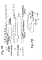
- FIG. 1 is a block diagram of a conventional system which provides a plurality of microprocessors exchanging bus access rights with each other, to which the present invention is applied.
- Fig. 1 designates a microprocessor which commands the bus access right
- 2a, 2b, and 2c are first, second, and third microprocessors, respectively, which receive the bus access right commands output by the microprocessor
- 3 designates a common memory
- 3a, 3b, and 3c are partial memories attached to the microprocessors 2a, 2b, and 2c respectively
- 4 is a common bus
- 5a, 5b, and 5c are bus access requests
- 6a, 6b, and 6c are affirmative acknowledgements for the requests.
- FIG. 2A shows diagrams of the operation of the conventional system shown in Fig. 1.
- Fig. 2A (a) shows a bus request signal 6b of the CPU 2b, (b) shows a bus request signal 6c of the CPU 2c, (c) shows an acknowledge signal of CPU 1 for CPU 2c, and (d) shows a change of the bus access right.
- CPU 2c requires the use of the bus 4 for CPU 1 at the time to during the bus cycle of CPU 2b as shown in (b), however, CPU 2b is using a bus at the time to as shown in (a), and thus CPU 1 does not issue the acknowledge signal to CPU 2c as shown in (c).
- a hold function is conventionally used.
- the microprocessor then requires a handshake function, such as hold hold acknowledge, or, request request grant, and a logic circuit for achieving this handshake function.
- the device issuing the hold request or a bus-request must wait until the microprocessor receiving the bus-request no longer requires access to the bus. This delay becomes an obstacle to carrying out an easy and rapid exchange of the bus access right or a direct memory access (DMA).
- DMA direct memory access
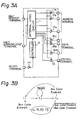
- Figure 3A is a block diagram of the microprocessor.
- 11 is an internal logic circuit
- 12 is a controller
- 14 is an inverter
- 17a N 17n, 18a ⁇ 18n and 19 are tristate output buffer circuits.
- Figure 3B is a chart for explaining the operation of the microprocessor shown in Fig. 3A.
- a bus cycle of the microprocessor of Fig. 3A includes three fundamental cycles T 1 , T 2 , T 3 , as shown in Fig. 3B.
- the address information is output.
- the value of the program counter (the value of the address output by T l ) is incremented (the address for outputting in the next bus cycle is calculated).
- the cycle T 3 the data is read or written.
- T I T 1 ⁇ T 2 ⁇ T 3 means that this cycle is not any of T 1 , T 2 , T 3 .
- the mark " . " signifies the AND logic.
- the output of the three state buffers 17 ⁇ 19 reaches a high impedance, and the bus is released to the other device.
- the bus cycle is looped at T 2 . At this time, the bus is not released. This ready signal is used for awaiting the completion of the access when the access time of the memory is large.
- the case in which the bus access right is removed at T 2 is considered.
- the address is output to 17a ⁇ 17n, and the address which is to be output next is counted in the program counter. Therefore, if the bus cycle is restarted from T 2 by again obtaining the bus access right, the address information before the bus access right is removed is already lost (that is, the next output address is set in the program counter). Therefore, the bus cycle executed immediately before the bus access right is removed is not completed, and the read or write of one piece of data is not performed.
- the change of the bus access right can be carried out without affecting the internal state of the microprocessor.
- the time at which the outputs of 17 to 19 reach a high impedance in response to the halt signal is after the bus cycle is completed at T 3 . Therefore, the other processor must wait until the time at which the bus cycle of the processor shown in Fig. 3A is completed.
- the present invention is intended to solve the above-mentioned problem.
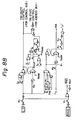
- the basic idea of the present invention is clearly shown in Fig. 2B.
- FIG. 2B shows diagrams for explaining the operation of the system shown in Fig. 1 according to the present invention.
- Fig. 2B shows a bus request signal (6c) of the CPU 2c, an output address ADD of the CPU 2c, and an output data DATA of the CPU 2c
- (b) shows an acknowledge signal 5c output from the CPU 1 to the CPU 2c and an acknowledge signal 5b output from the CPU 1 to the CPU 2b
- (c) shows an output address ADD' of the CPU 2b and an output data DATA' of the CPU 2b
- the acknowledge signal 5b is output from the CPU 2b in immediate response to the bus request of the CPU 2c, so that the bus access right is transferred from CPU 2b to CPU 2c.
- the bus request right 6c is released at the time t l . Consequently, the bus access right is again given to CPU 2b.
- one bus cycle of a CPU is formed with three basic cycles T 1 ⁇ T 3 mentioned above, the bus access right of CPU 2b is forcibly removed during the execution of T l .
- T' 1 shows the basic cycle using the held address A 1 and the held data D l .
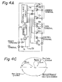
- Figure 4A shows a block diagram of the first embodiment of the present invention.
- lla is an internal logic circuit (CPC)
- 12a is a control circuit
- 13 is a gate
- 14 and 15 are inverters
- 16 is a gate
- 19a, 19b are tristate output buffer circuits.
- a CS terminal is provided which inputs a CS signal (chip select signal).
- the output states of the tristate output circuits 17a ⁇ 17n, 18a ⁇ 18m, and 19a, 19b are, via the gate, forcibly rendered to a high impedance state regardless of the processing state in the internal logic circuit lla.
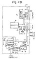
- Figure 4B is a block diagram showing details of the internal logic circuit lla shown in Fig. 4A.
- 31 is a register, 32 a program counter, 33 an address register, 34 a data register, 35 an arithmetic unit, 36 a state counter, 37 a bus cycle enable flag register, and 38 a status flip-flop.
- address calculated from the content of the registers 31 and/or program counter is stored in the address register 33 and these content of the register 31 or output of the ALU is stored in the data register 34, and is output from the address register 33 and the data register 34 (write cycle).
- the characteristic feature of the circuit of Fig. 4B is the provision of a state counter 36, address register 33, and data register 34.
- the state counter in Fig. 4B forms the timing signal T 1 ⁇ T3 which is used for the state transition shown in Fig. 4C.
- the timing signals T 1 ⁇ T 3 shown in Fig. 4B correspond to the basic cycle shown in Fig. 4C, and T is same as in Fig. 3B.
- the differences between Fig. 4C and Fig. 3B are as follows. When the signal supplied to the CS terminal is low, that is, CS ( * ) reaches a high impedance, it is looped at the basic cycle T 2 , and after CS becomes low, the bus cycle is backed from T 2 to T 1 (T l l in Fig. 2C) and is restarted from T l .
- the state counter advances internally to T 2 to become in a loop state.
- the data address immediately before the bus cycle is interrupted is held in the address register 33 and data register 34. Therefore, if the bus cycle is interrupted, the data address before the bus cycle is interrupted is not erased.
- the state counter 36 in Fig. 4B is operated as shown below.
- the bus cycle enable When the bus cycle enable is set (the output of the enable flag 37 is at a high level), when T 3 is placed at a high level, the output of G 3 also is at a high level, and this is returned to an input of the state counter via G 2 .
- the state counter responds to the output of G 2 , and this G 2 output is placed at the state T 1 of the basic cycle. Further, the signal T 1 ⁇ T 2 ⁇ T 3 showing the state not belonging to the basic cycle T, , T 2 , T3 (idle cycle T I ) is input to G 31 .
- the state counter transfers the output to the state T l of the basic cycle.
- the state counter receives the signal from the controller 12a and remains (loops) in the state T 2 of the basic cycle
- the signal * (refer to Fig. 4A) is at a high level
- the output of G 1 is at a high level
- the output of the state counter is transfered to the state T 1 of the basic cycle.
- the status flip-flop 38 outputs a high level signal or low level signal in accordance with whether it is a read or write operation.
- T 2 output from the state counter is high, in accordance of the output of the status flip flop, one of the outputs of G 5 or G 6 reaches a high level.
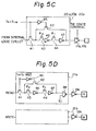
- Figure 5A shows a block diagram of the second embodiment of the present invention.
- llb is an internal logic circuit, 12 a control circuit, 13b a gate, 14 and 15 inverters, and 16 a gate.
- the other elements having the same symbol as those of Fig. 4A are the same elements as in the circuit shown in Fig. 4A.
- Figure 5A shows the case of a time sharing bus wherein the bus is commonly used as a data bus and an address bus.
- the register is commonly used as a data bus and an address bus.
- the register used in the present invention is shown in Fig. 5D.
- the register in Fig. 5C conventionally used, is not suitable for the present invention, and the register shown in Fig. 9 is used as mentioned hereinafter.
- Figure 5B is a block diagram showing details of the internal logic circuit llb shown in Fig. 5. In Fig. 5B, 31, 34, 35, and 38 in Fig. 4B are omitted.
- M 1 , M2 are multiplexers and, in accordance with the output of G 7 ⁇ G 9 , select the address or data and outputs it to an internal A/D bus.
- the internal A/D bus is connected to 20a ⁇ 20n.
- Reference numeral 40 shows a tristate counter, which forms the signal for effecting the state transfer shown in Fig. 7B mentioned hereinafter.
- the mark "+” shows a logical sum and the mark "•” shows a logical product.
- T 3 •Wait + T 2 + T' 2 means that the logically produced signal T 3 and the Wait signal are logically summed with the signal T 2 and the signal T 1 2 .
- the outputs G 7 ⁇ G 9 are input to the multiplexers M 1 , M2 as the control signal, synchronizing the output T 1 , T 3 , T 4 of the tristate counter 40 with the clock signal CLK.
- FIG. 6A One cycle in two cycle pipeline of the conventional address data time sharing bus and a status diagram thereof are shown in Figs. 6A and 6B.
- T 1 ⁇ T 4 designate basic cycle
- ⁇ 1 and ⁇ 2 designate a clock cycle timing and one bus cycle is formed by the basic cycles T 1 to T 4 .
- (c) is a timing relating to the A 1 address, Data, and A 2 Address
- (d) is a Ready signal
- (e) shows a state in the internal bus.
- the value of the program counter and the value to be added to the value of the program counter are set in an adder.
- one bus cycle is formed by T 1 ⁇ T 4 , and if the ready signal shown in Fig. 6A is high level, the bus cycle loops at the timing T 3 .
- the address is calculated at the timing T 4 , the result thereof is loaded to the output register, the address is output and the data is loaded to the output register at the timing T, , and the data is output at the timing T 2 (in the write cycle).
- the state counter of Fig. 5B is formed, so that the state transfer shown in Fig. 7B is carried out.
- the output register of each bit may be constructed as the circuit shown in Fig. 5C.
- Fig. 5C when the transistor 41 becomes ON, the data is input via the transistor 43, and at this time, the transistor 42 is in an OFF state.
- the transistor 41 becomes OFF the transistor 42 becomes ON, the feedback loop is formed from the output of the transistor 47 to the input of the transistor 43, and the latch is effected so that the data is held.
- the output register is formed as shown in Fig. 9 so as to hold both the data and address.
- This bus cycle is also realized by the circuit shown in Fig. 5D.
- 41, 42, 43, and 44 designate field effect transistors (FET's), and 45, 46 and 47 designate inverters, respectively.
- An input signal T4 + T 1 x W for the inverter 45 is supplied from a state counter in the internal logic circuit.
- W designates a write signal.
- Figure 7A designates a state cycle diagram in the embodiment of the address data time sharing bus according to the present invention
- Fig. 7B designates the state diagram thereof.
- the characteristic feature of the present invention is to provide timings T '1 , T' 2 , and the relationship between these timings T' 1 , T'2 and the other timings T 1 ⁇ T 4 is formed by the state counter 40 in the internal logic circuit llb in Fig. 5.
- the circuit for forming the relationship between these timings will be explained by referring to Figs. 8A and 8B.
- a 1 is output to the internal A/D bus, and is output externally at the following T 1 .
- D 1 is output to the internal bus, and preparation is made to output D 1 externally.
- the signal OUTPUT ENABLE is low (enable state) at least until the time when the bus cycle is completed.
- the state of the state counter advances to T 3 , the address A 1 , D 1 output in the internal bus is held in 20a ⁇ 20n in Fig. 5A, and the state counter stops (i.e., loops) at T 3 as shown in Fig. 7B.
- CS reaches a high level
- the OUTPUT ENABLE reaches a low level (enable)
- the state of the state counter is then transfered to T' 1 , T' 2 .
- the operation which is carried out in the basic cycle T' 1 , T I 2 is the same as T, , T 2 , and the data and the address output at this time is the address A, and the data D held during CS is at a low level.
- the interrupted bus cycle is restarted from the beginning.
- Figure 8A is a detailed circuit of the state counter 40 in the internal circuit and Fig. 8B shows a detailed circuit for obtaining the timing T' 31 and the three state control signal.
- 50a ⁇ 50g designate a D type flip-flop circuit
- T 4 .R designates a write at the timing T 4
- the timing T 3 is obtained in the circuit shown in Fig. 8B.
- the timing T 1 , T' 1 , and T 4 in Fig. 8A are supplied to the registers 20a ⁇ 20n in Fig. 5A.
- the internal circuit of these registers is shown in Fig. 9.
- Fig. 8A CLK is a clock input terminal, D is a data input terminal, and OUT is a data output terminal; g 10 ⁇ g 16 is circuit for forming a logical signal by the logic of each input signal. For example, g 10 effects a logical AND of T 3 and T 3 , and in g 10 , the AND output of g 10 , T 2 and T' are logically OR ed. As a result, the signal T 3 ⁇ Wait + T 2 + T' 2 is output from g ll .
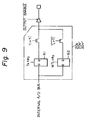
- reference numerals 61, 62 represent D type flip-flops.
- the flip-flop 61 holds the address and the flip-flop 62 holds the write data T 4 x ⁇ 1 is a clock signal for 61. Therefore, the address is supplied from the internal A/D bus to D.FF 61 synchronized with the clock ⁇ 2 in the basic cycle T 4 .
- the write data is supplied from the internal A/D bus to D.FF 62 synchronized with the clock ⁇ 2 in the basic cycle T 1 .
- W is a write control signal.
- the address held in the flip-flop 61 is output via the transfer gate to the output buffer at the basic cycle T 1 or T' 1 .
- the data held in the flip-flop 62 is output via the transfer gate at the basic cycle except for T 1 and T' 1 .
- Figure 10 is a concrete embodiment of the circuit including the registers in Fig. 9, the tristate output buffer circuits 17a, 17b, ...., and an output buffer 63.
- circuit 60 is a control circuit driven by a state counter included in the internal logic circuit.
- This circuit 60 includes a gate 70, inverters 70a, 70b, and 70c, FET's 71a, 71b, 71c, 71d, 71e, 71f, 71g, and 71h, and the output thereof is supplied to gate circuits 72a, 72b of the register.
- the FET circuit 61 includes FET's 73a, 73b, and 73c, and inverters 74a, 74b, and 74c, and the FF circuit 62 included FET's 75a, 75b, and 75c and inverters 76a, 76b, and 76c.
- the tristate gate circuits 17a, 17b, ... include an FET 80, inverters 81a, 81b, FET's 82, 83, 84a ⁇ 84c, 85a ⁇ 85c, 86a and 86b, and an inverter 87.
- an OUTPUT ENABLE signal high is supplied to the circuits 17a, 17b, ... , the transistor 80 is placed in an ON state, the input level of the inverter is at a high level and the output level of the inverter is at a low level, so that the output of the inverter 87 is at a high level. Therefore, the drain of the transistors 86a, 86b is at a low level, and the output of the output buffer 63 is at a high impedance state.
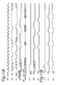
- Fig. 11A and 11B The timing charts practically measured in the system according to the present invention are shown in Fig. 11A and 11B.
- Fig. llA (a) shows a clock cycle actually at the timing ⁇ 2 , (b) shows a chip enable signal, (c) shows a wait signal, and (d) is a three state control signal generated in the circuit shown in Fig. 8.
- (e) is a signal in the write cycle in an A/D bus
- (f) is a request signal, that is, a bus cycle request signal, generated for commencing the instruction fetch or by an execution of the instruction.
- One request signal sometimes generates several bus cycles, and is at an active high level during bus cycle caused by the request, and is at a low level at the timing T 1 of the last bus cycle.
- Fig. 11A (g) is a retry signal and (h) is the signal T 31 ' generated in the circuit shown in Fig. 8B.
- FIG. 11B shows the timing T 4
- (j) and (k) are signals OA and OB, respectively, which are the outputs of the control circuit 60 shown in Fig. 10.
- the processor when the external device requiring the bus is allowed to use the bus, the processor makes the necessary signal to a high impedance, and when the input signal returns to an active state, the processor completes the bus cycle. This is very effective when the processor receives a bus request requiring a high priority and a rapid response, and the means for rapidly exchanging the bus is provided. Further, in the simple system, a simple and clear bus exchanging means is provided so that the size of the logic circuit can be reduced.
- the present invention is especially effective, when the data is output by dividing the data at a bus having a restricted data width, for example, data of 16 bits, 32 bits is output to an 8 bit bus by diving it twice or 4 times. That is, in the conventional method, the change of the bus access right must wait until the time when two bus cycles or four bus cycles are completed. However, in the present invention, this necessity can be eliminated.
Landscapes
- Engineering & Computer Science (AREA)
- Theoretical Computer Science (AREA)
- Physics & Mathematics (AREA)
- General Engineering & Computer Science (AREA)
- General Physics & Mathematics (AREA)
- Bus Control (AREA)
- Memory System (AREA)
- Semiconductor Integrated Circuits (AREA)
Applications Claiming Priority (2)
| Application Number | Priority Date | Filing Date | Title |
|---|---|---|---|
| JP109477/84 | 1984-05-31 | ||
| JP59109477A JPH0690700B2 (ja) | 1984-05-31 | 1984-05-31 | 半導体集積回路 |
Publications (3)
| Publication Number | Publication Date |
|---|---|
| EP0166248A2 true EP0166248A2 (de) | 1986-01-02 |
| EP0166248A3 EP0166248A3 (en) | 1988-09-14 |
| EP0166248B1 EP0166248B1 (de) | 1992-08-26 |
Family
ID=14511228
Family Applications (1)
| Application Number | Title | Priority Date | Filing Date |
|---|---|---|---|
| EP85106559A Expired - Lifetime EP0166248B1 (de) | 1984-05-31 | 1985-05-29 | Integrierte Halbleiterschaltung zum Austausch von Buszugriffberechtigungen zwischen Mikroprozessoren |
Country Status (5)
| Country | Link |
|---|---|
| US (1) | US4819158A (de) |
| EP (1) | EP0166248B1 (de) |
| JP (1) | JPH0690700B2 (de) |
| KR (1) | KR900007002B1 (de) |
| DE (1) | DE3586551T2 (de) |
Cited By (3)
| Publication number | Priority date | Publication date | Assignee | Title |
|---|---|---|---|---|
| EP0428330A2 (de) * | 1989-11-13 | 1991-05-22 | International Business Machines Corporation | Rechnerschnittstellenschaltung |
| EP0587370A1 (de) * | 1992-09-09 | 1994-03-16 | Digital Equipment Corporation | Verfahren und Vorrichtung zur gemeinsamen Nutzung von Software zwischen mehreren Steuerwerken |
| GB2326065A (en) * | 1997-06-05 | 1998-12-09 | Mentor Graphics Corp | Dual mode master/slave system on IC |
Families Citing this family (9)
| Publication number | Priority date | Publication date | Assignee | Title |
|---|---|---|---|---|
| US5179678A (en) * | 1987-09-08 | 1993-01-12 | Nec Corporation | Address/control signal input circuit for a cache controller which clamps the address/control signals to predetermined logic level clamp signal is received |
| JPH0786870B2 (ja) * | 1988-04-15 | 1995-09-20 | 株式会社日立製作所 | コプロセツサのデータ転送制御方法およびその回路 |
| US5440749A (en) * | 1989-08-03 | 1995-08-08 | Nanotronics Corporation | High performance, low cost microprocessor architecture |
| JP2762138B2 (ja) * | 1989-11-06 | 1998-06-04 | 三菱電機株式会社 | メモリコントロールユニット |
| JPH05324544A (ja) * | 1992-05-15 | 1993-12-07 | Hitachi Ltd | バス制御方法 |
| JP4030216B2 (ja) * | 1999-03-09 | 2008-01-09 | インターナショナル・ビジネス・マシーンズ・コーポレーション | マイクロプロセッサとマイクロプロセッサを含むシステム及びマイクロプロセッサのバスサイクル制御方法 |
| US8956161B2 (en) | 2008-11-04 | 2015-02-17 | Duane C Keller | Article and method for controlling oral-originated systemic disease |
| US8905760B2 (en) * | 2008-11-04 | 2014-12-09 | Duane C. Keller | Methods and systems for progressively treating and controlling oral periopathogens causing systemic inflammations |
| US8591229B2 (en) | 2010-12-16 | 2013-11-26 | Duane C. Keller | Devices and methods for creating a positive pressure environment for treatment of oral biofilms associated with periodontal disease |
Citations (2)
| Publication number | Priority date | Publication date | Assignee | Title |
|---|---|---|---|---|
| EP0009678A1 (de) * | 1978-10-02 | 1980-04-16 | International Business Machines Corporation | Ein-/Ausgabevorrichtung für Computer |
| US4348722A (en) * | 1980-04-03 | 1982-09-07 | Motorola, Inc. | Bus error recognition for microprogrammed data processor |
Family Cites Families (7)
| Publication number | Priority date | Publication date | Assignee | Title |
|---|---|---|---|---|
| JPS5248440A (en) * | 1975-10-15 | 1977-04-18 | Toshiba Corp | Memory access control system |
| US4112490A (en) * | 1976-11-24 | 1978-09-05 | Intel Corporation | Data transfer control apparatus and method |
| US4240138A (en) * | 1978-10-03 | 1980-12-16 | Texas Instruments Incorporated | System for direct access to a memory associated with a microprocessor |
| JPS58169248A (ja) * | 1982-03-30 | 1983-10-05 | Fujitsu Ltd | 入力条件セレクタ付プログラムカウンタ制御方式 |
| US4488228A (en) * | 1982-12-03 | 1984-12-11 | Motorola, Inc. | Virtual memory data processor |
| US4602327A (en) * | 1983-07-28 | 1986-07-22 | Motorola, Inc. | Bus master capable of relinquishing bus on request and retrying bus cycle |
| US4720811A (en) * | 1985-04-26 | 1988-01-19 | Hitachi, Ltd. | Microprocessor capable of stopping its operation at any cycle time |
-
1984
- 1984-05-31 JP JP59109477A patent/JPH0690700B2/ja not_active Expired - Lifetime
-
1985
- 1985-05-29 DE DE8585106559T patent/DE3586551T2/de not_active Expired - Fee Related
- 1985-05-29 EP EP85106559A patent/EP0166248B1/de not_active Expired - Lifetime
- 1985-05-30 US US06/739,338 patent/US4819158A/en not_active Expired - Lifetime
- 1985-05-31 KR KR1019850003804A patent/KR900007002B1/ko not_active IP Right Cessation
Patent Citations (2)
| Publication number | Priority date | Publication date | Assignee | Title |
|---|---|---|---|---|
| EP0009678A1 (de) * | 1978-10-02 | 1980-04-16 | International Business Machines Corporation | Ein-/Ausgabevorrichtung für Computer |
| US4348722A (en) * | 1980-04-03 | 1982-09-07 | Motorola, Inc. | Bus error recognition for microprogrammed data processor |
Non-Patent Citations (1)
| Title |
|---|
| MICROPROCESSORS AND MICROSYSTEMS, vol. 3, no. 9, November 1979, pages 413-420, IPC Business Press, New York, US; A. CLEMENTS: "Computer system buses" * |
Cited By (7)
| Publication number | Priority date | Publication date | Assignee | Title |
|---|---|---|---|---|
| EP0428330A2 (de) * | 1989-11-13 | 1991-05-22 | International Business Machines Corporation | Rechnerschnittstellenschaltung |
| EP0428330A3 (en) * | 1989-11-13 | 1992-11-04 | International Business Machines Corporation | Computer interface circuit |
| AU638495B2 (en) * | 1989-11-13 | 1993-07-01 | International Business Machines Corporation | Bus master interface circuit with transparent preemption of a data transfer operation |
| EP0587370A1 (de) * | 1992-09-09 | 1994-03-16 | Digital Equipment Corporation | Verfahren und Vorrichtung zur gemeinsamen Nutzung von Software zwischen mehreren Steuerwerken |
| US5408612A (en) * | 1992-09-09 | 1995-04-18 | Digital Equipment Corporation | Microprocessor system for selectively accessing a processor internal register when the processor has control of the bus and partial address identifying the register |
| GB2326065A (en) * | 1997-06-05 | 1998-12-09 | Mentor Graphics Corp | Dual mode master/slave system on IC |
| GB2326065B (en) * | 1997-06-05 | 2002-05-29 | Mentor Graphics Corp | A scalable processor independent on-chip bus |
Also Published As
| Publication number | Publication date |
|---|---|
| JPH0690700B2 (ja) | 1994-11-14 |
| EP0166248B1 (de) | 1992-08-26 |
| KR900007002B1 (ko) | 1990-09-25 |
| EP0166248A3 (en) | 1988-09-14 |
| DE3586551D1 (de) | 1992-10-01 |
| DE3586551T2 (de) | 1993-02-11 |
| US4819158A (en) | 1989-04-04 |
| JPS6111872A (ja) | 1986-01-20 |
| KR850008567A (ko) | 1985-12-18 |
Similar Documents
| Publication | Publication Date | Title |
|---|---|---|
| EP0166272B1 (de) | Buszugriff für Prozessor | |
| US4811202A (en) | Quadruply extended time multiplexed information bus for reducing the `pin out` configuration of a semiconductor chip package | |
| EP0409285B1 (de) | Verfahren und Vorrichtung zur Datenübertragung zwischen Prozessorelementen | |
| EP0172038A2 (de) | Informationsprozessor | |
| US4819158A (en) | Microprocessor with an interruptable bus cycle | |
| KR950009455A (ko) | 디지탈 신호처리 프로세서 | |
| US4348722A (en) | Bus error recognition for microprogrammed data processor | |
| US4835684A (en) | Microcomputer capable of transferring data from one location to another within a memory without an intermediary data bus | |
| JPS6297036A (ja) | 計算機システム | |
| JP2822782B2 (ja) | シングルチップマイクロコンピュータ | |
| US5410721A (en) | System and method for incrementing a program counter | |
| US6928494B1 (en) | Method and apparatus for timing-dependant transfers using FIFOs | |
| JPH051504B2 (de) | ||
| JPS61245255A (ja) | 不揮発性メモリ装置 | |
| JPS63118969A (ja) | 情報処理装置 | |
| JP2657947B2 (ja) | データ処理装置 | |
| JPS62296637A (ja) | シリアルデ−タの受信装置 | |
| JPH04109351A (ja) | Dmaコントローラ | |
| JPS58205258A (ja) | デ−タ処理装置 | |
| JPS5987549A (ja) | マイクロプログラム制御方式 | |
| JPS58215778A (ja) | バツフア記憶制御方式 | |
| JPH01154234A (ja) | 割込み制御装置 | |
| JPS63279351A (ja) | Dma転送制御装置 | |
| JPS59114638A (ja) | 高速演算素子のready信号発生方式 | |
| JPS58178467A (ja) | デ−タ転送装置 |
Legal Events
| Date | Code | Title | Description |
|---|---|---|---|
| PUAI | Public reference made under article 153(3) epc to a published international application that has entered the european phase |
Free format text: ORIGINAL CODE: 0009012 |
|
| AK | Designated contracting states |
Designated state(s): DE FR GB |
|
| PUAL | Search report despatched |
Free format text: ORIGINAL CODE: 0009013 |
|
| AK | Designated contracting states |
Kind code of ref document: A3 Designated state(s): DE FR GB |
|
| 17P | Request for examination filed |
Effective date: 19881214 |
|
| 17Q | First examination report despatched |
Effective date: 19901001 |
|
| GRAA | (expected) grant |
Free format text: ORIGINAL CODE: 0009210 |
|
| AK | Designated contracting states |
Kind code of ref document: B1 Designated state(s): DE FR GB |
|
| PGFP | Annual fee paid to national office [announced via postgrant information from national office to epo] |
Ref country code: FR Payment date: 19920828 Year of fee payment: 9 |
|
| REF | Corresponds to: |
Ref document number: 3586551 Country of ref document: DE Date of ref document: 19921001 |
|
| ET | Fr: translation filed | ||
| PGFP | Annual fee paid to national office [announced via postgrant information from national office to epo] |
Ref country code: GB Payment date: 19930518 Year of fee payment: 9 |
|
| PLBE | No opposition filed within time limit |
Free format text: ORIGINAL CODE: 0009261 |
|
| STAA | Information on the status of an ep patent application or granted ep patent |
Free format text: STATUS: NO OPPOSITION FILED WITHIN TIME LIMIT |
|
| PGFP | Annual fee paid to national office [announced via postgrant information from national office to epo] |
Ref country code: DE Payment date: 19930724 Year of fee payment: 9 |
|
| 26N | No opposition filed | ||
| PG25 | Lapsed in a contracting state [announced via postgrant information from national office to epo] |
Ref country code: GB Effective date: 19940529 |
|
| GBPC | Gb: european patent ceased through non-payment of renewal fee |
Effective date: 19940529 |
|
| PG25 | Lapsed in a contracting state [announced via postgrant information from national office to epo] |
Ref country code: FR Effective date: 19950131 |
|
| PG25 | Lapsed in a contracting state [announced via postgrant information from national office to epo] |
Ref country code: DE Effective date: 19950201 |
|
| REG | Reference to a national code |
Ref country code: FR Ref legal event code: ST |