EP0153854A2 - Bildherstellungsverfahren - Google Patents
Bildherstellungsverfahren Download PDFInfo
- Publication number
- EP0153854A2 EP0153854A2 EP85301231A EP85301231A EP0153854A2 EP 0153854 A2 EP0153854 A2 EP 0153854A2 EP 85301231 A EP85301231 A EP 85301231A EP 85301231 A EP85301231 A EP 85301231A EP 0153854 A2 EP0153854 A2 EP 0153854A2
- Authority
- EP
- European Patent Office
- Prior art keywords
- organic compound
- pattern film
- vapour
- film
- ion beam
- Prior art date
- Legal status (The legal status is an assumption and is not a legal conclusion. Google has not performed a legal analysis and makes no representation as to the accuracy of the status listed.)
- Granted
Links
Images


Classifications
-
- G—PHYSICS
- G03—PHOTOGRAPHY; CINEMATOGRAPHY; ANALOGOUS TECHNIQUES USING WAVES OTHER THAN OPTICAL WAVES; ELECTROGRAPHY; HOLOGRAPHY
- G03F—PHOTOMECHANICAL PRODUCTION OF TEXTURED OR PATTERNED SURFACES, e.g. FOR PRINTING, FOR PROCESSING OF SEMICONDUCTOR DEVICES; MATERIALS THEREFOR; ORIGINALS THEREFOR; APPARATUS SPECIALLY ADAPTED THEREFOR
- G03F1/00—Originals for photomechanical production of textured or patterned surfaces, e.g., masks, photo-masks, reticles; Mask blanks or pellicles therefor; Containers specially adapted therefor; Preparation thereof
- G03F1/68—Preparation processes not covered by groups G03F1/20 - G03F1/50
- G03F1/72—Repair or correction of mask defects
- G03F1/74—Repair or correction of mask defects by charged particle beam [CPB], e.g. focused ion beam
-
- Y—GENERAL TAGGING OF NEW TECHNOLOGICAL DEVELOPMENTS; GENERAL TAGGING OF CROSS-SECTIONAL TECHNOLOGIES SPANNING OVER SEVERAL SECTIONS OF THE IPC; TECHNICAL SUBJECTS COVERED BY FORMER USPC CROSS-REFERENCE ART COLLECTIONS [XRACs] AND DIGESTS
- Y10—TECHNICAL SUBJECTS COVERED BY FORMER USPC
- Y10S—TECHNICAL SUBJECTS COVERED BY FORMER USPC CROSS-REFERENCE ART COLLECTIONS [XRACs] AND DIGESTS
- Y10S438/00—Semiconductor device manufacturing: process
- Y10S438/942—Masking
- Y10S438/947—Subphotolithographic processing
Definitions
- This invention relates to processes for forming pattern films required, for example, in correcting photomasks during the fabrication of semiconductor devices.
- Masks and reticules for use in the manufacture of semiconductors are made by etching patterns through exposure to light.
- the process presents problems because of defects the patterns tend to develop. These defects are classified into two groups, unwanted pattern portions left unremoved which are called black-spot defects and portions needed but unintentionally etched away, called white-sport defects.
- White-sport defects are repaired by the use of an organic compound and irradiation with an ion beam.
- Two ways of doing this have been proposed so far.
- One typical way consists in applying an organic film such as photoresist to a sample and then irradiating each portion having a white-spot defect with a focused ion beam to polymerise or carbonise the organic film of the irradiated portion.
- the film polymerised or carbonised in this manner possesses an excellent light-shielding property and adhesion strength, which render it suitable as a material for correcting the white-spot defect.
- the process has drawbacks including the necessity of the time-consuming step of applying the organic film and of equipment large enough to handle such a high energy, well in excess of 100 keV, of the focused ion beam required for the irradiation.
- the other typical way of correcting white-spot defects with an organic compound and ion beam irradiation involves directing a vapour stream of an organic compound against each white-spot defect with concurrent irradiation of the surface portion with a focused ion beam, whereby the organic compound particles are polymerised or carbonised as a solid deposit on the defect.
- This second process is advantageous over the first in that it eliminates the step of application of the organic film and simplifies the equipment because of less energy requirement, i.e. below 30 keV, for the acceleration of ions for irradiation.
- the kinds of organic compound thus far proposed for use in the second process have included vacuum pump oils, organo-metallic compounds such as trimethylaluminium, and bisbenzene complexes such as [Cr(C 6 H 6 ) 2 ].
- vacuum pump oil When vacuum pump oil is used in remedying white-spot defects, its low vapour pressure at ordinary temperature (300 0 K), i.e. below 10 -6 Torr, makes the supply of the oil constituent molecules for film forming by polymerisation or carbonisation insufficient. Consequently, the rate of film build-up to a desired thickness is low. If the vacuum pump oil were to be heated to raise its vapour pressure for a faster increase in film thickness, it would condense on the sample surface.
- the present invention seeks to overcome the difficulties of the conventional processes for forming pattern films by forming a pattern film of less than one micron thickness rapidly by the use of an organic compound with good stability and extremely low toxicity.
- a process for forming a pattern film which comprises irradiating a specific portion of a sample with a focused ion beam in an atmosphere where the vapour of an organic compound is present, thereby polymerising or carbonising the organic compound on the specific portion to form a desired pattern film thereon characteristed in that said organic compound has a vapour pressure at 300 K between 1 x 10 -4 and 5 x 10 Torr.
- Said organic compound may be a tri- or tetracyclic aromatic compound.
- Preferably said organic compound has a molecular weight between 200 and 400.
- Said organic compound may consist mainly of a hydrocarbon compound and is free from any metal atom.
- Said organic compound may be phenanthrene, pyrene, methylphenanthrene, fluoranthene, anthrone or triphenylmethane.
- the number of organic compound molecules reacted by irradiation with one ion must be between 2 and 7.
- Average current density of irradiation with an ion beam is between 1 x 10 -3 and 1 x 10 -5 A/cm 2 .
- the organic compound molecules to be polymerised or carbonised are supplied to a support plate at a rate between 1 x 10 and 1 x 10 16 atoms/cm 2 sec. If the organic compound molecules are supplied at a rate of 1 x 10 13 atoms/cm 2 sec or below, there is too greater a volume of irradiation by the low beam.
- the rate of pattern film build-up to the desired thickness is low because of the spattering effect.
- the pattern film is not formed on the support plate which is spatter etched.
- the organic compound molecules are supplied at a rate of 10 16 atoms/cm 2 sec or above, the adherence of the pattern film on the support plate and its light shielding property are insufficient.
- An ion beam generator 4 comprises a bright ion source such as a liquid metal ion source and an ion optical system for heating, polarising, and focusing ions generated by the source.
- the focused ion beam 5 produced by the source is used to scan the area of the element omission 31 to effect ion irradiation at a constant rate.
- a source 6 feeding an organic compound includes a heater that control the source temperature and thereby adjusts the quantity of vapour 7 of the organic compound to be delivered to the element omission.
- the tempearture of the support plate 1 is at ordinary level (room temperature, 300°K).
- the vapour 7 of the organic compound mostly deposits on the support plate 1. It is polymerised or carbonised by irradiation with the ion beam 5.
- Figure 2b shows a pattern film 8 formed in this way on the element omission 31.
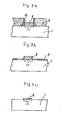
- Figure 3a illustrates a pattern film formed using an organic compound having a vapour pressure of 1 x 10 -4 Torr or below at room temperature (300°K).
- Figure 3b illustrates a pattern film formed by a process according to the present invention with an organic compound having a vapour pressure between 1 x 10 -4 and 5 x 10 -3 Torr at room temperature (300°K).
- Figure 3c illustrates a pattern film formed using organic compound having a vapour pressure of 5 x 10 -3 Torr or above at room temperature (300°K).
- the conditions of the ion beam 5 for irradiation and of the support plate 1 are the same in Figures 3a, 3b, 3c.
- the organic compound deposited on the support plate 1 forms an organic compound layer 9 because of its low evaporation rate.
- the portion irradiated with the ion beam 5 is reduced in thickness to a denser solid mass, lower in height than the original layer 9 and is polymerised or carbonised to form the pattern film 8.
- incomplete polymerised or carbonised organic compound layer portions 10 develop along the boundaries between the organic compound layer 9 and the pattern film 8. These portions make microfine processing difficult or can fall off where the bond strength is insufficient, producing unwanted shadows or causing other troubles in a subsequent stage of selective exposure of the pattern on a semiconductor wafer.
- the vapour of an organic compound having a vaour pressure in the range as specified by the present invention i.e. between 1 x 10 4 and 5 x 10 Torr at 300°K
- the organic compound delivered in vapour form against the support plate 1 deposits on the surface, remains there for some time, and then evaporates.
- a suitable amount of the organic compound vapour is supplied, and it is polymerised or carbonised by the next scan.
- the pattern film 8 grows to a desired thickness, e.g. 1 micron. Outside a spot 11 at which the organic compound is directed, the organic compound vapour forms only a negligibly thin organic compound layer 9.
- the organic compound layer 9 will evaporate substantially completely, leaving no obstacle behind which would hamper the formation of the pattern film.
- the organic compound has a vapour pressure of 5 x 10 -3 Torr or above at 300°K and so evaporates immediately after deposition on the Support plate 1. Consequently, the supply of the organic compound molecules for film forming must be 10 15 atoms/cm2 sec or greater so that it is necessary that the organic compound molecules are retained in a vacuum chamber.
- the pressure in the vacuum chamber thus increases using an ordinary vacuum system (vacuum rate of about 100 litre/sec). Therefore, the vapour of the organic compound has a deliterious influence on the ion source and the life of the apparatus.
- the organic compound has a vapour pressure of 5 x 10 -3 Torr or above and the pattern film is formed when the pressure in the pressure chamber is 1 x 10 -6 Torr or below to avoid this influence.
- the volume of the organic compound is too small for the pattern film element omission to obtain an adequate rate of film build-up to the desired thickness.
- organic compounds for a process according to the present invention for forming a pattern film include tri-or tetracyclic aromatic compounds such as phenanthrene, pyrene, methylphenanthrene, fluoranthene, anthrone and triphenylmethane. These organic compounds have vapour pressures at ordinary temperature (300 K ) between 1 x 10 -4 and 5 x 10 -3 Torr. Moreover, they are free from metal atoms, stable, and only slightly toxic. Organic compounds other than tri- and tetracyclic aromatic compounds but having molecular weights of 200 to 400 are useful also since their vapour pressures at ordinary temperature (300°K) are between 1 x 10 -4 and 5 x 10 -3 Torr.
- Figure 4a shows a sensible image obtained by light transmission through a sample on a support plate of clear glass and having a pattern of about 800 ⁇ -thick chromium layer drawn thereon but yet to be formed with a pattern film by a process according to the present invention.
- Figure 4b there is formed a pattern film area by a process according to the present invention, measuring 6.7 mm by 6.7 mm on an exposed glass portion 8 ⁇ m square in size of the sample in Figure 4a.
- a focused ion beam of Ga + was used for the irradiation, the acceleration voltage being 20kV, and probe current being 0.13 nA.
- the organic compound applied was pyrene heated to 80°C.
- the pattern film thus formed was 1400 i thick and provided adequate shield against light transmission, allowing the pattern film to have sharply defined edges.
- the rate of thickness build-up of the pattern film was 69 i/sec with a 200 ⁇ m-long scanning line of the ion beam at the acceleration voltage of 20 kV and with the probe current as 0.13 nA.
- the pattern film widths were of the order of submicrons.
- the physical and chemical adhesion strength of the pattern film obtained in this way are about the same as or more than those of the chromium film, which is well known in the art.
- the thickness of the pattern film that provides an optical density of 2.8 was approximately 2000 A for visible light and below 1000 A for ultraviolet rays. Under the aforedescribed film-forming conditions, therefore, it is possible to form a 200 ⁇ m-long, submicron-wide pattern film within 20 seconds by exposure to far-ultraviolet rays.
- the process according to the present invention for forming a film pattern in this way is particularly suited for producing microfine pattern films. It is also possible, of course, to form a larger area of pattern film at a faster rate by irradiation with a focused ion beam of a larger diameter and with a higher probe current.
- the present invention permits pattern film formation in a single step that concludes within a short period of time and to microfine patterns less than one micron in width. This makes possible a substantial reduction in the number of process stages otherwise required. Further advantages are the ease with which the organic compound is handled and the possibility of designing an apparatus of reasonable, rationalised construction for the purpose of carrying out a process according to the present invention.
Applications Claiming Priority (2)
| Application Number | Priority Date | Filing Date | Title |
|---|---|---|---|
| JP59038131A JPS60182726A (ja) | 1984-02-29 | 1984-02-29 | パタ−ン膜形成方法 |
| JP38131/84 | 1984-02-29 |
Related Child Applications (2)
| Application Number | Title | Priority Date | Filing Date |
|---|---|---|---|
| EP88201038.2 Division-Into | 1985-02-25 | ||
| EP88201038A Division EP0304969A3 (de) | 1984-02-29 | 1985-02-25 | Bildherstellungsverfahren |
Publications (3)
| Publication Number | Publication Date |
|---|---|
| EP0153854A2 true EP0153854A2 (de) | 1985-09-04 |
| EP0153854A3 EP0153854A3 (en) | 1987-09-30 |
| EP0153854B1 EP0153854B1 (de) | 1991-05-02 |
Family
ID=12516883
Family Applications (2)
| Application Number | Title | Priority Date | Filing Date |
|---|---|---|---|
| EP85301231A Expired - Lifetime EP0153854B1 (de) | 1984-02-29 | 1985-02-25 | Bildherstellungsverfahren |
| EP88201038A Withdrawn EP0304969A3 (de) | 1984-02-29 | 1985-02-25 | Bildherstellungsverfahren |
Family Applications After (1)
| Application Number | Title | Priority Date | Filing Date |
|---|---|---|---|
| EP88201038A Withdrawn EP0304969A3 (de) | 1984-02-29 | 1985-02-25 | Bildherstellungsverfahren |
Country Status (4)
| Country | Link |
|---|---|
| US (2) | US4874632A (de) |
| EP (2) | EP0153854B1 (de) |
| JP (1) | JPS60182726A (de) |
| DE (1) | DE3582690D1 (de) |
Cited By (5)
| Publication number | Priority date | Publication date | Assignee | Title |
|---|---|---|---|---|
| EP0316111A2 (de) * | 1987-11-09 | 1989-05-17 | AT&T Corp. | Maskenkorrektur |
| US4908226A (en) * | 1988-05-23 | 1990-03-13 | Hughes Aircraft Company | Selective area nucleation and growth method for metal chemical vapor deposition using focused ion beams |
| US5273849A (en) * | 1987-11-09 | 1993-12-28 | At&T Bell Laboratories | Mask repair |
| EP1079273A2 (de) * | 1999-08-27 | 2001-02-28 | Lucent Technologies Inc. | Maskenreparatur |
| US6395347B1 (en) * | 1993-11-30 | 2002-05-28 | Seiko Instruments Inc. | Micromachining method for workpiece observation |
Families Citing this family (9)
| Publication number | Priority date | Publication date | Assignee | Title |
|---|---|---|---|---|
| JPS60182726A (ja) * | 1984-02-29 | 1985-09-18 | Seiko Instr & Electronics Ltd | パタ−ン膜形成方法 |
| JPS62281349A (ja) * | 1986-05-29 | 1987-12-07 | Seiko Instr & Electronics Ltd | 金属パタ−ン膜の形成方法及びその装置 |
| JPH0664338B2 (ja) * | 1988-02-02 | 1994-08-22 | 三菱電機株式会社 | 薄膜パターンの修正方法およびその方法によって修正された露光用マスク |
| US5225771A (en) * | 1988-05-16 | 1993-07-06 | Dri Technology Corp. | Making and testing an integrated circuit using high density probe points |
| US5362591A (en) * | 1989-10-09 | 1994-11-08 | Hitachi Ltd. Et Al. | Mask having a phase shifter and method of manufacturing same |
| US4985714A (en) * | 1990-01-22 | 1991-01-15 | Polaroid Corporation | Film dispenser with articulated catcher |
| JPH04324085A (ja) * | 1991-04-23 | 1992-11-13 | Toshiba Corp | 製氷装置 |
| US6261723B1 (en) | 1999-03-04 | 2001-07-17 | International Business Machines Corporation | Transfer layer repair process for attenuated masks |
| DE10230675B4 (de) | 2002-07-04 | 2007-01-25 | Infineon Technologies Ag | Verfahren zur Herstellung von Phasenschiebermasken |
Citations (1)
| Publication number | Priority date | Publication date | Assignee | Title |
|---|---|---|---|---|
| EP0075949A2 (de) * | 1981-09-30 | 1983-04-06 | Hitachi, Ltd. | Ionenstrahl-Bearbeitungsapparat und Methode zur Korrektur von Maskenfehlern |
Family Cites Families (28)
| Publication number | Priority date | Publication date | Assignee | Title |
|---|---|---|---|---|
| US3117022A (en) * | 1960-09-06 | 1964-01-07 | Space Technhology Lab Inc | Deposition arrangement |
| US3364087A (en) * | 1964-04-27 | 1968-01-16 | Varian Associates | Method of using laser to coat or etch substrate |
| GB1168641A (en) * | 1966-05-19 | 1969-10-29 | British Iron Steel Research | Formation of Polymer Coatings on Substrates. |
| US3516855A (en) * | 1967-05-29 | 1970-06-23 | Ibm | Method of depositing conductive ions by utilizing electron beam |
| US3949106A (en) * | 1969-12-29 | 1976-04-06 | Toyo Boseki Kabushiki Kaisha | Method for producing isotropic pyrolisis carbon coatings |
| US3801366A (en) * | 1971-02-16 | 1974-04-02 | J Lemelson | Method of making an electrical circuit |
| US4042006A (en) * | 1973-01-05 | 1977-08-16 | Siemens Aktiengesellschaft | Pyrolytic process for producing a band-shaped metal layer on a substrate |
| US3930155A (en) * | 1973-01-19 | 1975-12-30 | Hitachi Ltd | Ion microprobe analyser |
| JPS4997690A (de) * | 1973-01-19 | 1974-09-14 | ||
| JPS52124883A (en) * | 1976-04-12 | 1977-10-20 | Mitsubishi Electric Corp | Local connection method of semiconductor crystal substrate and metal wiring |
| JPS5846055B2 (ja) * | 1977-04-30 | 1983-10-14 | 三菱電機株式会社 | ホトマスクの欠陥修正法 |
| US4264642A (en) * | 1978-12-11 | 1981-04-28 | Lord Corporation | Deposition of thin film organic coatings by ion implantation |
| JPS5632143A (en) * | 1979-08-24 | 1981-04-01 | Sanyo Electric Co Ltd | Manufacture of photomask |
| US4405435A (en) * | 1980-08-27 | 1983-09-20 | Hitachi, Ltd. | Apparatus for performing continuous treatment in vacuum |
| JPS5787128A (en) * | 1980-11-19 | 1982-05-31 | Toshiba Corp | Correcting method of mask |
| US4357364A (en) * | 1981-04-27 | 1982-11-02 | Rockwell International Corporation | High rate resist polymerization method |
| US4488506A (en) * | 1981-06-18 | 1984-12-18 | Itt Industries, Inc. | Metallization plant |
| JPS586133A (ja) * | 1981-07-03 | 1983-01-13 | Mitsubishi Electric Corp | 微細パタ−ン形成装置 |
| JPS5992526A (ja) * | 1982-11-19 | 1984-05-28 | Hitachi Ltd | パタ−ン形成方法及び装置 |
| JPS59168652A (ja) * | 1983-03-16 | 1984-09-22 | Hitachi Ltd | 素子修正方法及びその装置 |
| DE3483982D1 (de) * | 1983-06-29 | 1991-02-28 | Siemens Ag | Verfahren zur herstellung einer elektrisch leitfaehigen verbindung und vorrichtung zur durchfuehrung eines solchen verfahrens. |
| JPH0830272B2 (ja) * | 1983-08-22 | 1996-03-27 | 日本電気株式会社 | 薄膜形成方法 |
| US4460436A (en) * | 1983-09-06 | 1984-07-17 | International Business Machines Corporation | Deposition of polymer films by means of ion beams |
| JPS6094728A (ja) * | 1983-10-27 | 1985-05-27 | Seiko Instr & Electronics Ltd | 荷電粒子ビームを用いた加工方法およびその装置 |
| JPS60182726A (ja) * | 1984-02-29 | 1985-09-18 | Seiko Instr & Electronics Ltd | パタ−ン膜形成方法 |
| JPS60196942A (ja) * | 1984-03-21 | 1985-10-05 | Hitachi Ltd | フオトマスク欠陥修正方法 |
| US4698236A (en) * | 1984-10-26 | 1987-10-06 | Ion Beam Systems, Inc. | Augmented carbonaceous substrate alteration |
| JPH0694728A (ja) * | 1992-09-09 | 1994-04-08 | Shimadzu Corp | 臨床検査装置のサンプルパレット |
-
1984
- 1984-02-29 JP JP59038131A patent/JPS60182726A/ja active Granted
-
1985
- 1985-02-25 DE DE8585301231T patent/DE3582690D1/de not_active Expired - Lifetime
- 1985-02-25 EP EP85301231A patent/EP0153854B1/de not_active Expired - Lifetime
- 1985-02-25 EP EP88201038A patent/EP0304969A3/de not_active Withdrawn
-
1986
- 1986-10-17 US US06/921,820 patent/US4874632A/en not_active Expired - Lifetime
-
1989
- 1989-10-24 US US07/426,430 patent/US5071671A/en not_active Expired - Lifetime
Patent Citations (1)
| Publication number | Priority date | Publication date | Assignee | Title |
|---|---|---|---|---|
| EP0075949A2 (de) * | 1981-09-30 | 1983-04-06 | Hitachi, Ltd. | Ionenstrahl-Bearbeitungsapparat und Methode zur Korrektur von Maskenfehlern |
Non-Patent Citations (3)
| Title |
|---|
| NUCLEAR INSTRUMENTS AND METHODS, vol. 182/183, 1981, pages 297-302, North-Holland Publishing Co., Amsterdam, NL; W. M\LLER et al.: "Carbon buildup by ion-induced polymerization under 100-400 keV H, He, and Li bombardment" * |
| PATENT ABSTRACTS OF JAPAN, vol. 3, no. 6 (E-85), 22nd January 1979; & JP-A-53 135 276 (MITSUBISHI DENKI K.K.) 25-11-1978 * |
| PATENT ABSTRACTS OF JAPAN, vol. 7, no. 76 (E-167)[1221], 30th March 1983; & JP-A-58 006 133 (MITSUBISHI DENKI K.K.) 13-01-1983 * |
Cited By (8)
| Publication number | Priority date | Publication date | Assignee | Title |
|---|---|---|---|---|
| EP0316111A2 (de) * | 1987-11-09 | 1989-05-17 | AT&T Corp. | Maskenkorrektur |
| EP0316111A3 (en) * | 1987-11-09 | 1989-09-27 | American Telephone And Telegraph Company | Mask repair |
| US5273849A (en) * | 1987-11-09 | 1993-12-28 | At&T Bell Laboratories | Mask repair |
| US4908226A (en) * | 1988-05-23 | 1990-03-13 | Hughes Aircraft Company | Selective area nucleation and growth method for metal chemical vapor deposition using focused ion beams |
| US6395347B1 (en) * | 1993-11-30 | 2002-05-28 | Seiko Instruments Inc. | Micromachining method for workpiece observation |
| EP1079273A2 (de) * | 1999-08-27 | 2001-02-28 | Lucent Technologies Inc. | Maskenreparatur |
| EP1079273A3 (de) * | 1999-08-27 | 2001-05-02 | Lucent Technologies Inc. | Maskenreparatur |
| US6368753B1 (en) | 1999-08-27 | 2002-04-09 | Agere Systems Guardian Corp. | Mask repair |
Also Published As
| Publication number | Publication date |
|---|---|
| JPS6322577B2 (de) | 1988-05-12 |
| EP0153854A3 (en) | 1987-09-30 |
| EP0304969A2 (de) | 1989-03-01 |
| EP0304969A3 (de) | 1989-10-11 |
| EP0153854B1 (de) | 1991-05-02 |
| DE3582690D1 (de) | 1991-06-06 |
| US5071671A (en) | 1991-12-10 |
| US4874632A (en) | 1989-10-17 |
| JPS60182726A (ja) | 1985-09-18 |
Similar Documents
| Publication | Publication Date | Title |
|---|---|---|
| EP0153854A2 (de) | Bildherstellungsverfahren | |
| US4405710A (en) | Ion beam exposure of (g-Gex -Se1-x) inorganic resists | |
| US4606932A (en) | Method for depositing a micron-size metallic film on a transparent substrate utilizing a laser | |
| US4548883A (en) | Correction of lithographic masks | |
| US6017658A (en) | Lithographic mask and method for fabrication thereof | |
| JPS58119641A (ja) | マスクのテスト方法 | |
| GB2172246A (en) | Pattern-forming method | |
| US4329410A (en) | Production of X-ray lithograph masks | |
| US5273849A (en) | Mask repair | |
| US4608332A (en) | Electron lithography mask manufacture | |
| Prewett et al. | Repair of opaque defects in photomasks using focused ion beams | |
| JP2867479B2 (ja) | レジストパターンの形成方法 | |
| US4027052A (en) | Fabrication of iron oxide pattern | |
| JPS6358446A (ja) | パタ−ン形成方法 | |
| JPH03129349A (ja) | フォトマスクの製法 | |
| US4647523A (en) | Production of a resist image | |
| WO1989007285A1 (en) | Integrated circuit micro-fabrication using dry lithographic processes | |
| Saitoh et al. | Practical results of photomask repair using focused ion beam technology | |
| EP0316111B1 (de) | Maskenkorrektur | |
| Caswell et al. | Formation of thin film circuits using preferential nucleation | |
| JPS6013432B2 (ja) | Al又はAl合金パタ−ンの形成方法 | |
| Okada et al. | Repairing x-ray masks with Ta absorbers using focused ion beams | |
| JPS649616B2 (de) | ||
| US3833396A (en) | Pattern delineation method and product so produced | |
| JP3154808B2 (ja) | マスク、マスク修正装置及びマスク修正方法 |
Legal Events
| Date | Code | Title | Description |
|---|---|---|---|
| PUAI | Public reference made under article 153(3) epc to a published international application that has entered the european phase |
Free format text: ORIGINAL CODE: 0009012 |
|
| AK | Designated contracting states |
Designated state(s): DE FR GB |
|
| PUAL | Search report despatched |
Free format text: ORIGINAL CODE: 0009013 |
|
| AK | Designated contracting states |
Kind code of ref document: A3 Designated state(s): DE FR GB |
|
| RAP1 | Party data changed (applicant data changed or rights of an application transferred) |
Owner name: SEIKO INSTRUMENTS INC. |
|
| 17P | Request for examination filed |
Effective date: 19880302 |
|
| 17Q | First examination report despatched |
Effective date: 19891018 |
|
| GRAA | (expected) grant |
Free format text: ORIGINAL CODE: 0009210 |
|
| AK | Designated contracting states |
Kind code of ref document: B1 Designated state(s): DE FR GB |
|
| REF | Corresponds to: |
Ref document number: 3582690 Country of ref document: DE Date of ref document: 19910606 |
|
| ET | Fr: translation filed | ||
| PLBE | No opposition filed within time limit |
Free format text: ORIGINAL CODE: 0009261 |
|
| STAA | Information on the status of an ep patent application or granted ep patent |
Free format text: STATUS: NO OPPOSITION FILED WITHIN TIME LIMIT |
|
| 26N | No opposition filed | ||
| REG | Reference to a national code |
Ref country code: GB Ref legal event code: 746 Effective date: 19931221 |
|
| REG | Reference to a national code |
Ref country code: GB Ref legal event code: 775O |
|
| REG | Reference to a national code |
Ref country code: GB Ref legal event code: IF02 |
|
| PGFP | Annual fee paid to national office [announced via postgrant information from national office to epo] |
Ref country code: FR Payment date: 20040210 Year of fee payment: 20 |
|
| PGFP | Annual fee paid to national office [announced via postgrant information from national office to epo] |
Ref country code: GB Payment date: 20040225 Year of fee payment: 20 |
|
| PGFP | Annual fee paid to national office [announced via postgrant information from national office to epo] |
Ref country code: DE Payment date: 20040304 Year of fee payment: 20 |
|
| PG25 | Lapsed in a contracting state [announced via postgrant information from national office to epo] |
Ref country code: GB Free format text: LAPSE BECAUSE OF EXPIRATION OF PROTECTION Effective date: 20050224 |
|
| REG | Reference to a national code |
Ref country code: GB Ref legal event code: PE20 |
|
| REG | Reference to a national code |
Ref country code: GB Ref legal event code: 732E |
|
| REG | Reference to a national code |
Ref country code: FR Ref legal event code: TP |