EP0149232B1 - Halbleiterbauelement mit einem metallischen Sockel - Google Patents
Halbleiterbauelement mit einem metallischen Sockel Download PDFInfo
- Publication number
- EP0149232B1 EP0149232B1 EP19840116238 EP84116238A EP0149232B1 EP 0149232 B1 EP0149232 B1 EP 0149232B1 EP 19840116238 EP19840116238 EP 19840116238 EP 84116238 A EP84116238 A EP 84116238A EP 0149232 B1 EP0149232 B1 EP 0149232B1
- Authority
- EP
- European Patent Office
- Prior art keywords
- semiconductor body
- semiconductor component
- semiconductor
- component according
- template
- Prior art date
- Legal status (The legal status is an assumption and is not a legal conclusion. Google has not performed a legal analysis and makes no representation as to the accuracy of the status listed.)
- Expired
Links
Images

Classifications
-
- H—ELECTRICITY
- H10—SEMICONDUCTOR DEVICES; ELECTRIC SOLID-STATE DEVICES NOT OTHERWISE PROVIDED FOR
- H10W—GENERIC PACKAGES, INTERCONNECTIONS, CONNECTORS OR OTHER CONSTRUCTIONAL DETAILS OF DEVICES COVERED BY CLASS H10
- H10W76/00—Containers; Fillings or auxiliary members therefor; Seals
- H10W76/10—Containers or parts thereof
- H10W76/12—Containers or parts thereof characterised by their shape
- H10W76/15—Containers comprising an insulating or insulated base
- H10W76/153—Containers comprising an insulating or insulated base having interconnections in passages through the insulating or insulated base
-
- H—ELECTRICITY
- H10—SEMICONDUCTOR DEVICES; ELECTRIC SOLID-STATE DEVICES NOT OTHERWISE PROVIDED FOR
- H10W—GENERIC PACKAGES, INTERCONNECTIONS, CONNECTORS OR OTHER CONSTRUCTIONAL DETAILS OF DEVICES COVERED BY CLASS H10
- H10W70/00—Package substrates; Interposers; Redistribution layers [RDL]
- H10W70/60—Insulating or insulated package substrates; Interposers; Redistribution layers
- H10W70/67—Insulating or insulated package substrates; Interposers; Redistribution layers characterised by their insulating layers or insulating parts
- H10W70/68—Shapes or dispositions thereof
- H10W70/6875—Shapes or dispositions thereof being on a metallic substrate, e.g. insulated metal substrates [IMS]
-
- F—MECHANICAL ENGINEERING; LIGHTING; HEATING; WEAPONS; BLASTING
- F02—COMBUSTION ENGINES; HOT-GAS OR COMBUSTION-PRODUCT ENGINE PLANTS
- F02B—INTERNAL-COMBUSTION PISTON ENGINES; COMBUSTION ENGINES IN GENERAL
- F02B1/00—Engines characterised by fuel-air mixture compression
- F02B1/02—Engines characterised by fuel-air mixture compression with positive ignition
- F02B1/04—Engines characterised by fuel-air mixture compression with positive ignition with fuel-air mixture admission into cylinder
-
- H—ELECTRICITY
- H10—SEMICONDUCTOR DEVICES; ELECTRIC SOLID-STATE DEVICES NOT OTHERWISE PROVIDED FOR
- H10W—GENERIC PACKAGES, INTERCONNECTIONS, CONNECTORS OR OTHER CONSTRUCTIONAL DETAILS OF DEVICES COVERED BY CLASS H10
- H10W72/00—Interconnections or connectors in packages
- H10W72/50—Bond wires
- H10W72/531—Shapes of wire connectors
- H10W72/5363—Shapes of wire connectors the connected ends being wedge-shaped
-
- H—ELECTRICITY
- H10—SEMICONDUCTOR DEVICES; ELECTRIC SOLID-STATE DEVICES NOT OTHERWISE PROVIDED FOR
- H10W—GENERIC PACKAGES, INTERCONNECTIONS, CONNECTORS OR OTHER CONSTRUCTIONAL DETAILS OF DEVICES COVERED BY CLASS H10
- H10W72/00—Interconnections or connectors in packages
- H10W72/50—Bond wires
- H10W72/551—Materials of bond wires
- H10W72/552—Materials of bond wires comprising metals or metalloids, e.g. silver
-
- H—ELECTRICITY
- H10—SEMICONDUCTOR DEVICES; ELECTRIC SOLID-STATE DEVICES NOT OTHERWISE PROVIDED FOR
- H10W—GENERIC PACKAGES, INTERCONNECTIONS, CONNECTORS OR OTHER CONSTRUCTIONAL DETAILS OF DEVICES COVERED BY CLASS H10
- H10W90/00—Package configurations
- H10W90/701—Package configurations characterised by the relative positions of pads or connectors relative to package parts
- H10W90/751—Package configurations characterised by the relative positions of pads or connectors relative to package parts of bond wires
- H10W90/753—Package configurations characterised by the relative positions of pads or connectors relative to package parts of bond wires between laterally-adjacent chips
-
- H—ELECTRICITY
- H10—SEMICONDUCTOR DEVICES; ELECTRIC SOLID-STATE DEVICES NOT OTHERWISE PROVIDED FOR
- H10W—GENERIC PACKAGES, INTERCONNECTIONS, CONNECTORS OR OTHER CONSTRUCTIONAL DETAILS OF DEVICES COVERED BY CLASS H10
- H10W90/00—Package configurations
- H10W90/701—Package configurations characterised by the relative positions of pads or connectors relative to package parts
- H10W90/751—Package configurations characterised by the relative positions of pads or connectors relative to package parts of bond wires
- H10W90/754—Package configurations characterised by the relative positions of pads or connectors relative to package parts of bond wires between a chip and a stacked insulating package substrate, interposer or RDL
-
- Y—GENERAL TAGGING OF NEW TECHNOLOGICAL DEVELOPMENTS; GENERAL TAGGING OF CROSS-SECTIONAL TECHNOLOGIES SPANNING OVER SEVERAL SECTIONS OF THE IPC; TECHNICAL SUBJECTS COVERED BY FORMER USPC CROSS-REFERENCE ART COLLECTIONS [XRACs] AND DIGESTS
- Y10—TECHNICAL SUBJECTS COVERED BY FORMER USPC
- Y10T—TECHNICAL SUBJECTS COVERED BY FORMER US CLASSIFICATION
- Y10T29/00—Metal working
- Y10T29/49—Method of mechanical manufacture
- Y10T29/49002—Electrical device making
- Y10T29/49117—Conductor or circuit manufacturing
- Y10T29/49124—On flat or curved insulated base, e.g., printed circuit, etc.
- Y10T29/4913—Assembling to base an electrical component, e.g., capacitor, etc.
- Y10T29/49133—Assembling to base an electrical component, e.g., capacitor, etc. with component orienting
Definitions
- the invention relates to a semiconductor device according to the preamble of the main claim.
- a semiconductor component in which a disk-shaped semiconductor body is soldered directly onto a metallic base is known, for example, from US Pat. No. 3,584,265. Furthermore, it is known to solder a disk-shaped semiconductor body onto a metallic base indirectly via an interposed carrier, which consists of electrically conductive material and is intended to compensate for the different coefficients of thermal expansion of the base and the semiconductor body.
- semiconductor components have become known in which the underside of the disk-shaped semiconductor body to be soldered to the metallic base forms a full-area electrical connection contact of the semiconductor body and in which at least one electrical connection contact, of which an electrical connection line is attached, is attached to the top of the disk-shaped semiconductor body leads to an outer connection conductor of the semiconductor component, which can be designed as a connection pin and is assigned to the electrical connection contact on the top side of the semiconductor body, which is narrowly limited in terms of area.
- the attachment of the electrical connection line can either be carried out using soldering technology or using bonding technology. In the case of such semiconductor components, it is necessary to fix the disk-shaped semiconductor body relative to the base with the aid of templates before the soldering process.
- connection conductors that lead from the outer connection conductors to the connection contacts on the top of the semiconductor body are attached to the semiconductor body and to the outer connection conductors using soldering technology, it is possible to equip these connection conductors with certain spring properties and with them to help the semiconductor body while of the soldering process to be pressed resiliently onto the metallic base (US Pat. No. 3,720,999), so that the template used for adjusting the semiconductor body on the base can be removed again before the soldering process, and mold removal problems with regard to the template after the soldering process are thus eliminated (US Pat 3,689,985, U.S. Patent 3,715,633 and U.S. Patent 3,711,752).
- the bond wires used here if the underside of the semiconductor body is soldered to the base, can only be attached to the top of the base after the soldering process, because they are used to fix the semiconductor body on the base during Soldering process can not be used.
- the shape template used to adjust the semiconductor body on the base can only be removed after the soldering process. Demolding problems occur in mass production. If the semiconductor body floats against the template during the soldering process, it can jam during the subsequent cooling process, and when the template is removed, crystal breaks can occur at the edge of the semiconductor body, which can impair the ability to block and the electrical function of the semiconductor body.
- the semiconductor component according to the invention with the characterizing features of the main claim has the advantage that a possible jamming of the disk-shaped semiconductor body in the cooling process following the soldering process with the soldering template is no longer harmful, because in contrast to the previously used molding template, which according to the Soldering process is removed again, is part of the semiconductor device.
- a molding template can be used which, if removed after the soldering process, can damage the lost soldering template but not the disk-shaped semiconductor body. Further advantages result from the subclaims.
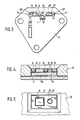
- FIG. 1 and 2 show a semiconductor component in plan view and in section, which contains a disk-shaped semiconductor body 1 designed as a transistor.
- the semiconductor body 1 has on its underside a first connection contact which extends over the entire underside. With this connection contact, the semiconductor body 1 is soldered onto a metallic socket 2, which forms part of the housing 3 of the semiconductor component and at the same time serves as a collector connection for the disk-shaped semiconductor body 1 designed as a transistor.
- Part of the housing 3 is also a cover cap 4, which is welded onto the metallic base 2.
- the upper part of the top cap 4 is cut off in FIG. 1.
- the semiconductor body 1 On its upper side, the semiconductor body 1 carries two further connection contacts, one of which forms the emitter connection and the other the base connection of the transistor.
- a bonding wire 5 leads to a post-shaped connection conductor 6, which is passed through the metallic base 2 in an insulated manner via a glass melt 7.
- a third post-like connecting conductor 6 ' which is only shown in FIG. 2, is butt-welded onto the base 2 and forms the outer collector connection of the transistor.
- the disk-shaped semiconductor body 1 is inserted into a recess 8 of a lost soldering template 9 soldered onto the metallic base 2.
- the edge length of the recess 8 is selected to be approximately 0.1 mm larger than the edge length of the semiconductor body 1.
- indentations 10 are provided on the circumference of the soldering template 9 and two knobs 11 are provided on the metallic base 2.
- the indentations 10 and the knobs 11 are arranged in relation to one another in such a way that the lost soldering template 9 can be placed immovably on the metallic base 2 in a defined position.
- the lost soldering template 9 is circular and is arranged concentrically with the cover cap 4 surrounding it.
- the two indentations 10 are diametrically opposite one another on the circumference of the lost soldering template 9 and the two knobs 11 are attached to the metallic base 2 in a corresponding position.
- indentations 10 can also be made at other points along the circumference of the lost soldering template 9 or can be replaced by differently designed recesses which can be made inside the soldering template.
- a further cutout 12 is provided in the lost soldering template 9 for the passage of the two post-like connecting conductors 6, which has a circular design and the diameter of which is selected such that the glass melts 7 , which receive the two connection conductors 6, are exposed, so that a short circuit between the different connections of the transistor is avoided.
- the lost soldering template 9 contains two further cutouts 13. Before the assembly is soldered, soldered soldering parts 9 have been inserted into these cutouts 13, which solder supplies for soldering the disk-shaped semiconductor body 1 and the lost soldering template 9 formed on the metallic base 2.
- the procedure for producing the semiconductor component according to FIGS. 1 and 2 is as follows:
- the base 2 which is already made of metal and already provided with the knobs 11 and with holes for the glass melts, onto which the post-like connecting conductor 6 ', which is also made of metal, is butt-welded, is first of all included on its entire surface, including that of the post-like connecting conductor 6' coated with a corrosion-resistant and solderable metallic layer, which preferably consists of nickel. Then the post-like connecting conductors 6 are melted into the bores of the metal base 2 and in this way are passed through the base 2 in an insulated manner with the aid of the glass melts 7.
- the lost soldering template 9 which is preferably made of copper and is nickel-plated, is placed on the base 2 and adjusted relative to the base 2 with the aid of the knobs 11 of the base 2 and the indentations 10 attached to it. Then, the disk-shaped semiconductor body 1 and in the recesses 13 a solder molded part, not shown in FIGS. 1 and 2, is inserted into the cutout 8 and the arrangement thus assembled is transported through the soldering furnace.
- the solder introduced into the recesses 13 in the form of the solder molded parts is melted and migrates under the action of the capillary force under the soldering template 9 and under the disk-shaped semiconductor body 1 and causes these two parts 9 and 1 to be soldered onto the metallic base 2 at the same time .
- the bonding wires 5 are attached in a special operation, which lead from the connection contacts on the upper side of the disk-shaped semiconductor body 1 to the post-like connection conductors 6.
- the semiconductor component completely contacted in this way is then provided with the cover cap 4, which is welded onto the metal base 2.
- the invention is not limited to the arrangement described with reference to FIGS. 1 and 2.
- a plurality of semiconductor bodies can also be soldered onto the metallic base 2 at the same time using a single lost soldering template which contains a special recess for each of these semiconductor bodies.
- FIG. 3 shows an example of an arrangement in which three platelet-shaped semiconductor bodies 1, 1 ', 1 "can be soldered onto a common metallic base using a single lost soldering template 9.
- recesses 8, 8', 8" are provided in the soldering template 9 .
- the adjustment is carried out with the aid of two knobs 11 attached to the base 2, which engage in further cutouts 10 ′ of the soldering template 9.
- a further cutout 13 serves to receive a solder molded part.
- FIGS. 4 and 5 show a semiconductor component being produced before soldering in accordance with a further proposal of the invention.
- a semiconductor body 1 designed as a transistor is to be soldered on to a metal base 2 in an insulated manner with its collector connection attached to the underside of the entire surface.
- a double-sided metallized ceramic plate 14 made of beryllium oxide is used for insulation, which is soldered between the system consisting of the lost soldering template 9 and the semiconductor body 1 on the one hand and the base 2 on the other hand.
- the metallization of the ceramic plate 14 can contain a gold coating as the top layer.
- a mold template 15 is placed on the metallic base 2. First, a solder molding 16 and then the ceramic plate 14 are placed in a recess in the mold template 15, which in this way comes to lie on the solder mold part 16 and completely fills the recess in the mold template 15 except for a narrow, left edge.
- a lost soldering template 9 is placed on the ceramic plate 14, the outer dimensions of which correspond exactly to those of the ceramic plate 14 and which has a cutout 8 for the semiconductor body 1 and a cutout 13 for a further solder molded part 17. After the soldering template 9 has been placed on the ceramic plate 14, the semiconductor body 1 and the solder molded part 17 are inserted into the recesses 8 and 13 provided in this template and the system thus assembled is then transported through the soldering furnace. Here the soldering takes place in the manner already described above.
- the recess 13 in the lost soldering template 9 can be omitted if, instead of the solder molding 17, a solder molding is used, which is placed under the semiconductor body 1 or under the lost soldering template 9, or if the lost soldering template 9 and / or the semiconductor body 1 on the respective one Underside is provided with a solder layer.
- the semiconductor body 1 soldered onto the metallic base 2 is insulated against it by the ceramic plate 14.
- the collector connection located on the underside of the semiconductor body 1 and the electrodes located on its top side (base and emitter connection) must be contacted from the top of the system, for which purpose the lost soldering template 9 is used.
- a thin metal wire for connecting the collector can be soldered or welded to this soldering template 9 in the same way as for the emitter and base contact.
- the lost soldering template 9 can be provided beforehand with a thin layer of aluminum or nickel, and when attaching the metal wire using soldering technology, with a thin layer of nickel.
- FIGS. 6 and 7 The finished component produced in this way is shown in FIGS. 6 and 7. All of the connecting wires led to the outside start here from the top of the system formed from the semiconductor body 1 and the lost soldering template 9.
- a bonding wire 5 leads from the emitter and base contact to a special post-like connecting conductor 6 which is passed through the base 2 in an insulated manner.
- the collector is also contacted via a bonding wire, which is denoted here by 5 'and leads from the lost soldering template 9 to a post-like connecting conductor 6' which, like the other two post-like connecting conductors 6, leads over a glass melt 7 is passed through the base 2 in an insulated manner.
Landscapes
- Die Bonding (AREA)
- Wire Bonding (AREA)
Description
- Die Erfindung betrifft ein Halbleiterbauelement nach der Gattung des Hauptanspruchs.
- Ein Halbleiterbauelement, bei dem ein scheibenförmiger Halbleiterkörper auf einen metallischen Sockel unmittelbar aufgelötet ist, ist beispielsweise aus der US-PS 3 584 265 bekannt. Ferner ist es bekannt, einen scheibenförmigen Halbleiterkörper auf einen metallischen Sockel mittelbar über einen dazwischengeschalteten Träger, der aus elektrisch leitendem Material besteht und die unterschiedlichen Wärmeausdehnungskoeffizienten von Sockel und Halbleiterkörper ausgleichen soll, aufzulöten.
- Weiterhin sind Halbleiterbauelemente bekanntgeworden, bei denen die mit dem metallischen Sockel zu verlötende Unterseite des scheibenförmigen Halbleiterkörpers einen ganzflächigen elektrischen Anschlusskontakt des Halbleiterkörpers bildet und bei denen ferner an der Oberseite des scheibenförmigen Halbleiterkörpers mindestens ein flächenmässig eng begrenzter elektrischer Anschlusskontakt angebracht ist, von dem eine elektrische Verbindungsleitung zu einem äusseren Anschlussleiter des Halbleiterbauelements führt, der als Anschlussstift ausgeführt sein kann und dem flächenmässig eng begrenzten elektrischen Anschlusskontakt an der Oberseite des Halbleiterkörpers zugeordnet ist. Das Anbringen der elektrischen Verbindungsleitung kann dabei entweder in Löttechnik oder in Bondtechnik ausgeführt werden. Bei derartigen Halbleiterbauelementen ist es notwendig, den scheibenförmigen Halbleiterkörper vor dem Lötprozess mit Hilfe von Schablonen relativ zu dem Sockel zu fixieren.
- Werden die elektrischen Verbindungsleitungen, die von den äusseren Anschlussleitern zu den Anschlusskontakten an der Oberseite des Halbleiterkörpers führen, am Halbleiterkörper und an den äusseren Anschlussleitern in Löttechnik angebracht, so besteht zwar die Möglichkeit, diese Anschlussleiter mit bestimmten Federeigenschaften auszustatten und mit ihrer Hilfe den Halbleiterkörper während des Lötprozesses an den metallischen Sockel federnd anzudrücken (US-PS 3 720 999), so dass die zur Justierung des Halbleiterkörpers auf dem Sockel verwendete Schablone vor dem Lötprozess wieder entfernt werden kann und Entformungsprobleme hinsichtlich der Schablone nach dem Lötprozess somit entfallen (US-PS 3 689 985, US-PS 3715633 und US-PS 3 711 752). Dieses Verfahren ist aber nur dann anwendbar, wenn der scheibenförmige Halbleiterkörper und die an seiner Oberseite angebrachten Anschlusskontakte verhältnismässig grossflächig ausgebildet sind und demzufolge an das Positionieren des Halbleiterkörpers relativ zum Sockel keine extrem hohen Anforderungen gestellt werden müssen. Ein Verrutschen des Halbleiterkörpers nach dem Entfernen der Schablone vor oder während des Lötprozesses kann aber hier nicht mit Sicherheit ausgeschlossen werden.
- Werden die elektrischen Verbindungsleitungen, die von den äusseren Anschlussleitern des Halbleiterbauelements zu den ihnen zugeordneten Anschlusskontakten an der Oberseite des Halbleiterkörpers führen, an dem Halbleiterkörper und an den zugehörigen äusseren Anschlussleitern in Bondtechnik angebracht (US-PS 4128802), was insbesondere bei sehr kleinflächigen Halbleiterkörpern oder bei solchen mit sehr vielen Anschlusskontakten der Fall ist, so können die hierbei verwendeten Bonddrähte, falls der Halbleiterkörper mit seiner Unterseite an den Sockel angelötet wird, erst nach dem Lötprozess an dessen Oberseite angebracht werden, weil sie zur Fixierung des Halbleiterkörpers auf dem Sockel während des Lötprozesses nicht herangezogen werden können. Die zur Justierung des Halbleiterkörpers auf dem Sockel verwendete Formschablone kann hierbei erst nach dem Lötprozess wieder entfernt werden. Dabei treten in einer Mengenfertigung Entformungsprobleme auf. Wenn der Halbleiterkörper während des Lötprozesses gegen die Schablone schwimmt, kann er sich beim anschliessenden Abkühlvorgang verklemmen, und beim Entfernen der Schablone können am Rand des Halbleiterkörpers Kristallbrüche auftreten, die die Sperrfähigkeit und die elektrische Funktion des Halbleiterkörpers beeinträchtigen können.
- Das erfindungsgemässe Halbleiterbauelement mit den kennzeichnenden Merkmalen des Hauptanspruchs hat demgegenüber den Vorteil, dass ein mögliches Verklemmen des scheibenförmigen Halbleiterkörpers bei dem sich an den Lötprozess anschliessenden Abkühlvorgang mit der Lötschablone nicht mehr schädlich ist, weil diese im Gegensatz zu der bislang verwendeten Formschablone, die nach dem Lötprozess wieder entfernt wird, Bestandteil des Halbleiterbauelementes ist. Zur Justierung der verlorenen Lötschablone und des scheibenförmigen Halbleiterkörpers kann gemäss einer möglichen Ausführung des Verfahrens zur Herstellung des erfindungsgemässen Halbleiterbauelements eine Formschablone verwendet werden, die jetzt bei ihrem Entfernen nach dem Lötprozess allenfalls die verlorene Lötschablone, nicht aber den scheibenförmigen Halbleiterkörper, beschädigen kann. Weitere Vorteile ergeben sich aus den Unteransprüchen.
- Ausführungsbeispiele des erfindungsgemässen Halbleiterbauelementes sind in der Zeichnung dargestellt und in der nachfolgenden Beschreibung näher erläutert. Es zeigen:
- Figur 1 ein erstes Ausführungsbeispiel eines Halbleiterbauelements nach der Erfindung mit abgeschnittener Deckkappe in der Draufsicht;
- Figur 2 einen Schnitt nach der Linie 11-11 der Figur 1;
- Figur 3 eine Anordnung zum Justieren und Verlöten eines zweiten Ausführungsbeispiels eines Halbleiterbauelements nach der Erfindung in der Draufsicht;
- Figur 4 einen Schnitt durch ein vormontiertes, noch nicht verlötetes Halbleiterbauelement mit einer Formschablone zum Justieren der verschiedenen Teile zueinander;
- Figur 5 eine Draufsicht auf die Anordnung nach Figur 4;
- Figur 6 ein drittes Ausführungsbeispiel eines Halbleiterbauelements nach der Erfindung mit abgeschnittener Deckkappe in der Draufsicht;
- Figur 7 einen Schnitt nach der Linie VII-VII der Figur 6.
- In den Figuren 1 und 2 ist ein Halbleiterbauelement in der Draufsicht und im Schnitt dargestellt, das einen als Transistor ausgebildeten scheibenförmigen Halbleiterkörper 1 enthält. Der Halbleiterkörper 1 trägt an seiner Unterseite einen ersten Anschlusskontakt, der sich über die ganze Unterseite erstreckt. Mit diesem Anschlusskontakt ist der Halbleiterkörper 1 auf einen metallischen Sokkel 2 aufgelötet, welcher einen Teil des Gehäuses 3 des Halbleiterbauelements bildet und gleichzeitig als Kollektoranschluss für den als Transistor ausgebildeten scheibenförmigen Halbleiterkörper 1 dient. Bestandteil des Gehäuses 3 ist ferner eine Deckkappe 4, die auf den metallischen Sockel 2 aufgeschweisst ist. Der obere Teil der Deckkappe 4 ist in Figur 1 abgeschnitten. An seiner Oberseite trägt der Halbleiterkörper 1 zwei weitere Anschlusskontakte, von denen der eine den Emitteranschluss und der andere den Basisanschluss des Transistors bildet. Von diesen beiden an der Oberseite angebrachten Anschlusskontakten führt je ein Bonddraht 5 zu einem pfostenförmigen Anschlussleiter 6, der über eine Glaseinschmelzung 7 isoliert durch den metallischen Sockel 2 hindurchgeführt ist. Ein dritter pfostenartiger Anschlussleiter 6', der nur in Figur 2 dargestellt ist, ist auf den Sockel 2 stumpf aufgeschweisst und bildet den äusseren Kollektoranschluss des Transistors.
- Der scheibenförmige Halbleiterkörper 1 ist in eine Aussparung 8 einer auf den metallischen Sockel 2 aufgelöteten verlorenen Lötschablone 9 eingefügt. Die Kantenlänge der Aussparung 8 ist dabei um ca. 0,1 mm grösser als die Kantenlänge des Halbleiterkörpers 1 gewählt. Um die verlorene Lötschablone 9 und damit den scheibenförmigen Halbleiterkörper 1 auf dem metallischen Sockel 2 justieren zu können, sind am Umfang der Lötschablone 9 Einbuchtungen 10 und an dem metallischen Sockel 2 zwei Noppen 11 vorgesehen. Die Einbuchtungen 10 und die Noppen 11 sind so zueinander angeordnet, dass die verlorene Lötschablone 9 auf den metallischen Sockel 2 in einer definierten Lage unverrückbar aufgesetzt werden kann. Beim Ausführungsbeispiel nach den Figuren 1 und 2 ist die verlorene Lötschablone 9 kreisförmig ausgebildet und konzentrisch zu der sie umschliessenden Deckkappe 4 angeordnet. Die beiden Einbuchtungen 10 sind dabei am Umfang der verlorenen Lötschablone 9 einander diametral gegenüberliegend und die beiden Noppen 11 an dem metallischen Sockel 2 in entsprechender Lage angebracht.
- Es versteht sich, dass diese Anordnung nur beispielhaft zu verstehen ist. Die Einbuchtungen 10 können auch an anderen Stellen des Umfangs der verlorenen Lötschablone 9 angebracht werden oder durch anders gestaltete Ausnehmungen ersetzt werden, die im Inneren der Lötschablone angebracht sein können.
- Ausser der Aussparung 8, die den scheibenförmigen Halbleiterkörper 1 aufnimmt, ist in der verlorenen Lötschablone 9 für den Durchtritt der beiden pfostenartigen Anschlussleiter 6 je eine weitere Aussparung 12 vorgesehen, die kreisförmig ausgebildet ist und deren Durchmesser jeweils so gewählt ist, dass auch die Glaseinschmelzungen 7, die die beiden Anschlussleiter 6 aufnehmen, freiliegen, so dass ein Kurzschluss zwischen den verschiedenen Anschlüssen des Transistors vermieden wird.
- In der Nähe der für den scheibenförmigen Halbleiterkörper 1 vorgesehenen Aussparung 8 enthält die verlorene Lötschablone 9 zwei weitere Aussparungen 13. In diese Aussparungen 13 sind vor dem Zusammenlöten der Anordnung Lotformteile eingelegt worden, die den Lotvorrat zum Anlöten des scheibenförmigen Halbleiterkörpers 1 und der verlorenen Lötschablone 9 an den metallischen Sockel 2 bildeten.
- Bei der Herstellung des Halbleiterbauelements nach den Figuren 1 und 2 wird wie folgt verfahren:
- Der aus Metall bestehende, bereits mit den Noppen 11 und mit Bohrungen für die Glaseinschmelzungen versehene Sockel 2, auf den bereits der ebenfalls aus Metall bestehende pfostenartige Anschlussleiter 6' stumpf aufgeschweisst ist, wird zunächst an seiner ganzen Oberfläche einschliesslich der des pfostenartigen Anschlussleiters 6' mit einer korrosionsbeständigen und lötfähigen metallischen Schicht, die vorzugsweise aus Nickel besteht, überzogen. Dann werden die pfostenartigen Anschlussleiter 6 in die Bohrungen des metallischen Sockels 2 eingeschmolzen und auf diese Weise mit Hilfe der Glaseinschmelzungen 7 durch den Sockel 2 isoliert hindurchgeführt.
- Nun wird die verlorene Lötschablone 9, die vorzugsweise aus Kupfer besteht und vernickelt ist, auf den Sockel 2 aufgesetzt und dabei mit Hilfe der Noppen 11 des Sockels 2 und der an ihr angebrachten Einbuchtungen 10 relativ zu dem Sockel 2 justiert. Dann wird in die Aussparung 8 der scheibenförmige Halbleiterkörper 1 und in die Aussparungen 13 jeweils ein in den Figuren 1 und 2 nicht dargestelltes Lotformteil eingelegt und die so montierte Anordnung durch den Lötofen transportiert.
- Beim Lötprozess wird das in die Aussparungen 13 in Form der Lotformteile eingebrachte Lot geschmolzen und wandert unter der Wirkung der Kapillarkraft unter die Lötschablone 9 und unter den scheibenförmigen Halbleiterkörper 1 und bewirkt, dass diese beiden Teile 9 und 1 gleichzeitig auf den metallischen Sockel 2 aufgelötet werden.
- Nach der Entnahme der so verlöteten Anordnung aus dem Lötofen werden in einem besonderen Arbeitsgang die Bonddrähte 5 angebracht, die von den Anschlusskontakten an der Oberseite des scheibenförmigen Halbleiterkörpers 1 zu den pfostenartigen Anschlussleitern 6 führen.
- Das auf diese Weise vollständig kontaktierte Halbleiterbauelement wird anschliessend mit der Deckkappe 4 versehen, die auf den metallischen Sockel 2 aufgeschweisst wird.
- Es versteht sich von selbst, dass die Erfindung nicht auf die anhand der Figuren 1 und 2 beschriebene Anordnung beschränkt ist. Anstelle eines einzigen Halbleiterkörpers können auch mehrere Halbleiterkörper gleichzeitig auf den metallischen Sockel 2 unter Verwendung einer einzigen verlorenen Lötschablone aufgelötet werden, die für jeden dieser Halbleiterkörper eine besondere Aussparung enthält. Auch besteht die Möglichkeit, den oder die Halbleiterkörper zusammen mit der verlorenen Lötschablone gegen den metallischen Sockel 2 elektrisch zu isolieren. Dies kann dadurch geschehen, dass in die Anordnung zwischen den metallischen Sockel und das aus Halbleiterkörper und Lötschablone bestehende System eine isolierende Platte, beispielsweise aus Keramik, eingelötet wird.
- Figur 3 zeigt beispielhaft eine Anordnung, bei der auf einen gemeinsamen metallischen Sockel drei plättchenförmige Halbleiterkörper 1, 1', 1" unter Verwendung einer einzigen verlorenen Lötschablone 9 aufgelötet werden können. Hierzu sind in der Lötschablone 9 Aussparungen 8, 8', 8" vorgesehen. Die Justierung erfolgt mit Hilfe zweier an dem Sockel 2 angebrachter Noppen 11, die in weitere Aussparungen 10' der Lötschablone 9 eingreifen. Zur Aufnahme eines Lotformteils dient eine weitere Aussparung 13.
- Die Figuren 4 und 5 zeigen ein in Herstellung begriffenes Halbleiterbauelement vor dem Verlöten gemäss einem weiteren Vorschlag der Erfindung. Bei diesem Ausführungsbeispiel ist vorgesehen, dass ein als Transistor ausgebildeter Halbleiterkörper 1 mit seinem an der Unterseite ganzflächig angebrachten Kollektoranschluss auf einen metallischen Sockel 2 isoliert aufgelötet werden soll. Zur Isolierung dient hierbei eine beidseitig metallisierte Keramikplatte 14 aus Berylliumoxid, die zwischen dem aus der verlorenen Lötschablone 9 und dem Halbleiterkörper 1 einerseits und den Sockel 2 andererseits bestehenden System eingelötet wird. Die Metallisierung der Keramikplatte 14 kann als oberste Schicht einen Goldüberzug enthalten.
- Auf den metallischen Sockel 2 wird eine Formschablone 15 aufgelegt. In eine Aussparung der Formschablone 15 wird zuerst ein Lotformteil 16 und anschliessend die Keramikplatte 14 eingelegt, die auf diese Weise auf das Lotformteii 16 zu liegen kommt und die in der Formschablone 15 befindliche Aussparung bis auf einen schmalen freigelassenen Rand vollständig ausfüllt. Auf die Keramikplatte 14 wird eine verlorene Lötschablone 9 aufgelegt, deren äussere Abmessungen genau denen der Keramikplatte 14 entsprechen und die eine Aussparung 8 für den Halbleiterkörper 1 und eine Aussparung 13 für ein weiteres Lotformteil 17 besitzt. Nach dem Auflegen der Lötschablone 9 auf die Keramikplatte 14 werden in die in dieser Schablone vorgesehenen Aussparungen 8 und 13 der Halbleiterkörper 1 und das Lotformteil 17 eingelegt und danach das so montierte System durch den Lötofen transportiert. Hier erfolgt die Verlötung in der bereits weiter oben beschriebenen Weise.
- Die Aussparung 13 in der verlorenen Lötschablone 9 kann entfallien, wenn anstelle des Lotformteils 17 ein Lotformteil verwendet wird, das unter den Halbleiterkörper 1 oder unter die verlorene Lötschablone 9 gelegt wird, oder wenn die verlorene Lötschablone 9 und/oder der Halbleiterkörper 1 an der jeweiligen Unterseite mit einer Lotschicht versehen ist.
- Der Unterschied gegenüber dem Ausführungsbeispiel nach den Figuren 1 und 2 besteht darin, dass beim vorliegenden Ausführungsbeispiel der auf den metallischen Sockel 2 aufgelötete Halbleiterkörper 1 gegen diesen durch die Keramikplatte 14 isoliert wird. Dies führt dazu, dass der an der Unterseite des Halbleiterkörpers 1 liegende Kollektoranschluss ebenso wie die an seiner Oberseite liegenden Elektroden (Basis- und Emitteranschluss) von der Oberseite des Systems her zu kontaktieren ist, wozu die verlorene Lötschablone 9 Verwendung findet. An dieser Lötschablone 9 kann ein dünner Metalldraht für den Anschluss des Kollektors in gleicher Weise wie für den Emitter- und Basiskontakt angelötet oder angeschweisst werden. Beim Anbringen des Metalldrahts in Bondtechnik (Schweissen) kann die verlorene Lötschablone 9 zuvor mit einer dünnen Schicht aus Aluminium oder Nickel, beim Anbringen des Metalldrahts in Löttechnik mit einer dünnen Schicht aus Nickel versehen werden.
- Das so hergestellte fertige Bauelement ist in den Figuren 6 und 7 dargestellt. Sämtliche nach aussen geführten Anschlussdrähte gehen hier von der Oberseite des aus dem Halbleiterkörper 1 und der verlorenen Lötschablone 9 gebildeten Systems aus. Wie beim Ausführungsbeispiel nach den Figuren 1 und 2 führt jeweils ein Bonddraht 5 vom Emitter- und Basiskontakt zu einem besonderen pfostenartigen Anschlussleiter 6, der isoliert durch den Sockel 2 hindurchgeführt ist. Im Gegensatz zu dem Ausführungsbeispiel nach den Figuren 1 und 2 ist auch der Kollektor über einen Bonddraht kontaktiert, der hier mit 5' bezeichnet ist und von der verlorenen Lötschablone 9 zu einem pfostenartigen Anschlussleiter 6' führt, der wie die beiden anderen pfostenartigen Anschlussleiter 6 über eine Glaseinschmelzung 7 isoliert durch den Sockel 2 hindurchgeführt ist.
Claims (11)
Applications Claiming Priority (2)
| Application Number | Priority Date | Filing Date | Title |
|---|---|---|---|
| DE19843401404 DE3401404A1 (de) | 1984-01-17 | 1984-01-17 | Halbleiterbauelement |
| DE3401404 | 1984-01-17 |
Publications (4)
| Publication Number | Publication Date |
|---|---|
| EP0149232A2 EP0149232A2 (de) | 1985-07-24 |
| EP0149232A3 EP0149232A3 (en) | 1987-02-04 |
| EP0149232B1 true EP0149232B1 (de) | 1988-10-26 |
| EP0149232B2 EP0149232B2 (de) | 1994-03-09 |
Family
ID=6225147
Family Applications (1)
| Application Number | Title | Priority Date | Filing Date |
|---|---|---|---|
| EP19840116238 Expired - Lifetime EP0149232B2 (de) | 1984-01-17 | 1984-12-22 | Halbleiterbauelement mit einem metallischen Sockel |
Country Status (4)
| Country | Link |
|---|---|
| US (1) | US4661835A (de) |
| EP (1) | EP0149232B2 (de) |
| JP (1) | JPH0799766B2 (de) |
| DE (2) | DE3401404A1 (de) |
Families Citing this family (37)
| Publication number | Priority date | Publication date | Assignee | Title |
|---|---|---|---|---|
| DE3717489A1 (de) * | 1987-05-23 | 1988-12-01 | Asea Brown Boveri | Leistungshalbleitermodul und verfahren zur herstellung des moduls |
| US5252856A (en) * | 1990-09-26 | 1993-10-12 | Nec Corporation | Optical semiconductor device |
| DE4107660C2 (de) * | 1991-03-09 | 1995-05-04 | Bosch Gmbh Robert | Verfahren zur Montage von Silizium-Plättchen auf metallischen Montageflächen |
| DE4135369A1 (de) * | 1991-10-26 | 1993-05-13 | Bosch Gmbh Robert | Testbarer piezoelektrischer beschleunigungssensor |
| DE4201931C1 (de) * | 1992-01-24 | 1993-05-27 | Eupec Europaeische Gesellschaft Fuer Leistungshalbleiter Mbh + Co.Kg, 4788 Warstein, De | |
| DE4235908A1 (de) * | 1992-10-23 | 1994-04-28 | Telefunken Microelectron | Verfahren zum Verlöten eines Halbleiterkörpers mit einem Trägerelement |
| DE4322715A1 (de) * | 1993-07-08 | 1995-01-12 | Bosch Gmbh Robert | Bauelementeinheit mit lunkerarmer Lötverbindung |
| ATE393319T1 (de) | 1998-09-03 | 2008-05-15 | Ge Novasensor Inc | Proportionale, mikromechanische vorrichtung |
| US7011378B2 (en) | 1998-09-03 | 2006-03-14 | Ge Novasensor, Inc. | Proportional micromechanical valve |
| US6523560B1 (en) | 1998-09-03 | 2003-02-25 | General Electric Corporation | Microvalve with pressure equalization |
| US6845962B1 (en) | 2000-03-22 | 2005-01-25 | Kelsey-Hayes Company | Thermally actuated microvalve device |
| US6505811B1 (en) | 2000-06-27 | 2003-01-14 | Kelsey-Hayes Company | High-pressure fluid control valve assembly having a microvalve device attached to fluid distributing substrate |
| US6581640B1 (en) | 2000-08-16 | 2003-06-24 | Kelsey-Hayes Company | Laminated manifold for microvalve |
| US20070251586A1 (en) * | 2003-11-24 | 2007-11-01 | Fuller Edward N | Electro-pneumatic control valve with microvalve pilot |
| WO2005084211A2 (en) * | 2004-02-27 | 2005-09-15 | Alumina Micro Llc | Hybrid micro/macro plate valve |
| KR20060109959A (ko) * | 2003-11-24 | 2006-10-23 | 알루미나 마이크로 엘엘씨 | 가변형 변위 압축기 제어용 마이크로밸브 장치 |
| US8011388B2 (en) | 2003-11-24 | 2011-09-06 | Microstaq, INC | Thermally actuated microvalve with multiple fluid ports |
| WO2005091820A2 (en) | 2004-03-05 | 2005-10-06 | Alumina Micro Llc | Selective bonding for forming a microvalve |
| US7156365B2 (en) * | 2004-07-27 | 2007-01-02 | Kelsey-Hayes Company | Method of controlling microvalve actuator |
| KR20070092328A (ko) * | 2005-01-14 | 2007-09-12 | 알루미나 마이크로 엘엘씨 | 가변용량형 압축기를 제어하기 위한 시스템 및 방법 |
| WO2008076388A1 (en) | 2006-12-15 | 2008-06-26 | Microstaq, Inc. | Microvalve device |
| WO2008121369A1 (en) | 2007-03-30 | 2008-10-09 | Microstaq, Inc. | Pilot operated micro spool valve |
| WO2008121365A1 (en) | 2007-03-31 | 2008-10-09 | Microstaq, Inc. | Pilot operated spool valve |
| US8662468B2 (en) | 2008-08-09 | 2014-03-04 | Dunan Microstaq, Inc. | Microvalve device |
| US8113482B2 (en) * | 2008-08-12 | 2012-02-14 | DunAn Microstaq | Microvalve device with improved fluid routing |
| CN102308131B (zh) | 2008-12-06 | 2014-01-08 | 盾安美斯泰克有限公司 | 流体流动控制组件 |
| WO2010117874A2 (en) | 2009-04-05 | 2010-10-14 | Microstaq, Inc. | Method and structure for optimizing heat exchanger performance |
| WO2011022267A2 (en) | 2009-08-17 | 2011-02-24 | Microstaq, Inc. | Micromachined device and control method |
| US9006844B2 (en) | 2010-01-28 | 2015-04-14 | Dunan Microstaq, Inc. | Process and structure for high temperature selective fusion bonding |
| US8956884B2 (en) | 2010-01-28 | 2015-02-17 | Dunan Microstaq, Inc. | Process for reconditioning semiconductor surface to facilitate bonding |
| US8996141B1 (en) | 2010-08-26 | 2015-03-31 | Dunan Microstaq, Inc. | Adaptive predictive functional controller |
| US8925793B2 (en) | 2012-01-05 | 2015-01-06 | Dunan Microstaq, Inc. | Method for making a solder joint |
| US9140613B2 (en) | 2012-03-16 | 2015-09-22 | Zhejiang Dunan Hetian Metal Co., Ltd. | Superheat sensor |
| US9188375B2 (en) | 2013-12-04 | 2015-11-17 | Zhejiang Dunan Hetian Metal Co., Ltd. | Control element and check valve assembly |
| US10319654B1 (en) * | 2017-12-01 | 2019-06-11 | Cubic Corporation | Integrated chip scale packages |
| CN113725085B (zh) * | 2021-08-31 | 2024-03-29 | 深圳技术大学 | 一种封装零件的装配工艺方法和封装零件 |
| US12255541B2 (en) * | 2022-05-23 | 2025-03-18 | Elmatek International Corp. | Power transistor conversion device |
Family Cites Families (20)
| Publication number | Priority date | Publication date | Assignee | Title |
|---|---|---|---|---|
| US2762001A (en) * | 1955-03-23 | 1956-09-04 | Globe Union Inc | Fused junction transistor assemblies |
| US3476985A (en) * | 1965-12-15 | 1969-11-04 | Licentia Gmbh | Semiconductor rectifier unit |
| US3419763A (en) * | 1966-10-31 | 1968-12-31 | Itt | High power transistor structure |
| DE1589543B2 (de) * | 1967-09-12 | 1972-08-24 | Robert Bosch Gmbh, 7000 Stuttgart | Halbleiterbauelement und verfahren zu seiner weichlotkontaktierung |
| FR1597186A (de) * | 1968-01-02 | 1970-06-22 | ||
| DE1903274A1 (de) * | 1969-01-23 | 1970-07-30 | Bosch Gmbh Robert | Verfahren zum Aufloeten eines Halbleiterkoerpers auf einen Traeger |
| FR2031024A5 (de) * | 1969-03-08 | 1970-11-13 | Bosch | |
| DE1961042C3 (de) * | 1969-12-05 | 1981-01-15 | Robert Bosch Gmbh, 7000 Stuttgart | Halbleiterbauelement |
| DE2022717A1 (de) * | 1970-05-09 | 1971-12-02 | Bosch Gmbh Robert | Halbleiterbauelement |
| US3715633A (en) * | 1971-07-15 | 1973-02-06 | J Nier | Semiconductor unit with integrated circuit |
| JPS5413010Y2 (de) * | 1974-09-25 | 1979-06-05 | ||
| JPS51163867U (de) * | 1975-06-19 | 1976-12-27 | ||
| JPS5273675A (en) * | 1975-12-16 | 1977-06-20 | Citizen Watch Co Ltd | Structure of die bonding |
| DE2610137A1 (de) * | 1976-03-11 | 1977-09-29 | Bosch Gmbh Robert | Generator mit freilaufdiode und spannungsregler |
| DE2814642A1 (de) * | 1978-04-05 | 1979-10-18 | Bosch Gmbh Robert | Verfahren zum befestigen mindestens eines halbleiterkoerpers auf einen traeger |
| US4285003A (en) * | 1979-03-19 | 1981-08-18 | Motorola, Inc. | Lower cost semiconductor package with good thermal properties |
| JPS57139932A (en) * | 1981-02-24 | 1982-08-30 | Nec Home Electronics Ltd | Insulating type semiconductor device |
| WO1982003294A1 (en) * | 1981-03-23 | 1982-09-30 | Inc Motorola | Semiconductor device including plateless package |
| JPS5856428A (ja) * | 1981-09-30 | 1983-04-04 | Fujitsu Ltd | 半導体装置 |
| FR2527837A1 (fr) * | 1982-05-25 | 1983-12-02 | Thomson Csf | Boitier d'encapsulation d'un dispositif semi-conducteur fonctionnant a tres haute tension, et son procede de fabrication |
-
1984
- 1984-01-17 DE DE19843401404 patent/DE3401404A1/de active Pending
- 1984-11-15 US US06/671,554 patent/US4661835A/en not_active Expired - Lifetime
- 1984-12-22 EP EP19840116238 patent/EP0149232B2/de not_active Expired - Lifetime
- 1984-12-22 DE DE8484116238T patent/DE3474884D1/de not_active Expired
-
1985
- 1985-01-16 JP JP60004175A patent/JPH0799766B2/ja not_active Expired - Lifetime
Also Published As
| Publication number | Publication date |
|---|---|
| JPH0799766B2 (ja) | 1995-10-25 |
| US4661835A (en) | 1987-04-28 |
| EP0149232A3 (en) | 1987-02-04 |
| EP0149232B2 (de) | 1994-03-09 |
| EP0149232A2 (de) | 1985-07-24 |
| DE3401404A1 (de) | 1985-07-25 |
| DE3474884D1 (en) | 1988-12-01 |
| JPS60163447A (ja) | 1985-08-26 |
Similar Documents
| Publication | Publication Date | Title |
|---|---|---|
| EP0149232B1 (de) | Halbleiterbauelement mit einem metallischen Sockel | |
| EP0762496B1 (de) | Leistungshalbleitermodul | |
| DE69503260T2 (de) | Verbindungsanordnung einer elektrischen Schaltung | |
| DE69026188T2 (de) | Elektrischer Verbinder | |
| DE102005024900B4 (de) | Leistungsmodul | |
| CH652533A5 (de) | Halbleiterbaustein. | |
| DE10129388A1 (de) | Elektronisches Bauteil und Verfahren zu seiner Herstellung | |
| DE102004021054B4 (de) | Halbleiterbauelement und Verfahren zu seiner Herstellung | |
| DE10008572B4 (de) | Verbindungseinrichtung für Leistungshalbleitermodule | |
| DE10205698A1 (de) | Leuchtdiode und Verfahren zur Herstellung Derselben | |
| DE1564107A1 (de) | Gekapselte Halbleiteranordnung | |
| DE1263190B (de) | Halbleiteranordnung mit einem in ein Gehaeuse eingeschlossenen Halbleiterkoerper | |
| EP1220314B1 (de) | Leistungshalbleitermodul | |
| DE3432449C2 (de) | ||
| DE3626151A1 (de) | Spannungszufuehrung fuer eine integrierte halbleiterschaltung | |
| DE3040867A1 (de) | Halbleiteranodnung und verfahren zu ihrer herstellung | |
| EP0069903B1 (de) | Elektrische Verbindungslasche für Halbleiterbauelemente | |
| DE2630320A1 (de) | Scheibenfoermige halbleiterzelle mit einem ringfoermigen gehaeuse | |
| DE10149774A1 (de) | Verfahren zum Verpacken von elektronischen Baugruppen und Mehrfachchipverpackung | |
| DE2143027C3 (de) | Halterung für ein HF-Halbleiterbauelement | |
| EP0152972B1 (de) | Kontaktierungssystem für 2-polige elektronische Bauelemente, insbesondere Halbleiterbauelemente | |
| DE4433503A1 (de) | Halbleiterbauelement mit Halbleiterchip und Verfahren zu dessen Herstellung | |
| DE3440925C2 (de) | ||
| DE102005036563B4 (de) | Elektronisches Bauteil | |
| DE2505882A1 (de) | Veraenderbarer kondensator |
Legal Events
| Date | Code | Title | Description |
|---|---|---|---|
| PUAI | Public reference made under article 153(3) epc to a published international application that has entered the european phase |
Free format text: ORIGINAL CODE: 0009012 |
|
| 17P | Request for examination filed |
Effective date: 19841222 |
|
| AK | Designated contracting states |
Designated state(s): DE FR GB IT NL |
|
| PUAL | Search report despatched |
Free format text: ORIGINAL CODE: 0009013 |
|
| AK | Designated contracting states |
Kind code of ref document: A3 Designated state(s): DE FR GB IT NL |
|
| 17Q | First examination report despatched |
Effective date: 19880322 |
|
| GRAA | (expected) grant |
Free format text: ORIGINAL CODE: 0009210 |
|
| AK | Designated contracting states |
Kind code of ref document: B1 Designated state(s): DE FR GB IT NL |
|
| GBT | Gb: translation of ep patent filed (gb section 77(6)(a)/1977) | ||
| REF | Corresponds to: |
Ref document number: 3474884 Country of ref document: DE Date of ref document: 19881201 |
|
| ET | Fr: translation filed | ||
| ITF | It: translation for a ep patent filed | ||
| PLBI | Opposition filed |
Free format text: ORIGINAL CODE: 0009260 |
|
| 26 | Opposition filed |
Opponent name: TELEFUNKEN ELECTRONIC GMBH Effective date: 19890725 |
|
| NLR1 | Nl: opposition has been filed with the epo |
Opponent name: TELEFUNKEN ELECTRONIC GMBH |
|
| ITTA | It: last paid annual fee | ||
| RAP4 | Party data changed (patent owner data changed or rights of a patent transferred) |
Owner name: ROBERT BOSCH GMBH |
|
| PLAB | Opposition data, opponent's data or that of the opponent's representative modified |
Free format text: ORIGINAL CODE: 0009299OPPO |
|
| R26 | Opposition filed (corrected) |
Opponent name: TEMIC TELEFUNKEN MICROELECTRONIC GMBH Effective date: 19890725 |
|
| NLXE | Nl: other communications concerning ep-patents (part 3 heading xe) |
Free format text: PAT.BUL.22/89 CORR.: TEMIC TELEFUNKEN MICROELECTRONIC GMBH |
|
| PUAH | Patent maintained in amended form |
Free format text: ORIGINAL CODE: 0009272 |
|
| STAA | Information on the status of an ep patent application or granted ep patent |
Free format text: STATUS: PATENT MAINTAINED AS AMENDED |
|
| 27A | Patent maintained in amended form |
Effective date: 19940309 |
|
| AK | Designated contracting states |
Kind code of ref document: B2 Designated state(s): DE FR GB IT NL |
|
| GBTA | Gb: translation of amended ep patent filed (gb section 77(6)(b)/1977) | ||
| ET3 | Fr: translation filed ** decision concerning opposition | ||
| NLR2 | Nl: decision of opposition | ||
| ITF | It: translation for a ep patent filed | ||
| NLR3 | Nl: receipt of modified translations in the netherlands language after an opposition procedure | ||
| PGFP | Annual fee paid to national office [announced via postgrant information from national office to epo] |
Ref country code: GB Payment date: 19981216 Year of fee payment: 15 |
|
| PGFP | Annual fee paid to national office [announced via postgrant information from national office to epo] |
Ref country code: FR Payment date: 19981218 Year of fee payment: 15 |
|
| PGFP | Annual fee paid to national office [announced via postgrant information from national office to epo] |
Ref country code: NL Payment date: 19981228 Year of fee payment: 15 |
|
| PG25 | Lapsed in a contracting state [announced via postgrant information from national office to epo] |
Ref country code: GB Free format text: LAPSE BECAUSE OF NON-PAYMENT OF DUE FEES Effective date: 19991222 |
|
| PG25 | Lapsed in a contracting state [announced via postgrant information from national office to epo] |
Ref country code: NL Free format text: LAPSE BECAUSE OF NON-PAYMENT OF DUE FEES Effective date: 20000701 |
|
| GBPC | Gb: european patent ceased through non-payment of renewal fee |
Effective date: 19991222 |
|
| PG25 | Lapsed in a contracting state [announced via postgrant information from national office to epo] |
Ref country code: FR Free format text: LAPSE BECAUSE OF NON-PAYMENT OF DUE FEES Effective date: 20000831 |
|
| NLV4 | Nl: lapsed or anulled due to non-payment of the annual fee |
Effective date: 20000701 |
|
| REG | Reference to a national code |
Ref country code: FR Ref legal event code: ST |
|
| PGFP | Annual fee paid to national office [announced via postgrant information from national office to epo] |
Ref country code: DE Payment date: 20040210 Year of fee payment: 20 |