EP0148951B1 - System zum kontrollieren von abnormalitäten in programmierbarem kontroller - Google Patents
System zum kontrollieren von abnormalitäten in programmierbarem kontroller Download PDFInfo
- Publication number
- EP0148951B1 EP0148951B1 EP84901808A EP84901808A EP0148951B1 EP 0148951 B1 EP0148951 B1 EP 0148951B1 EP 84901808 A EP84901808 A EP 84901808A EP 84901808 A EP84901808 A EP 84901808A EP 0148951 B1 EP0148951 B1 EP 0148951B1
- Authority
- EP
- European Patent Office
- Prior art keywords
- address
- signal
- address setting
- elements
- memory
- Prior art date
- Legal status (The legal status is an assumption and is not a legal conclusion. Google has not performed a legal analysis and makes no representation as to the accuracy of the status listed.)
- Expired
Links
- 230000005856 abnormality Effects 0.000 title claims description 17
- 230000004044 response Effects 0.000 claims description 4
- 238000001514 detection method Methods 0.000 abstract description 6
- 238000011835 investigation Methods 0.000 abstract 1
- 238000010586 diagram Methods 0.000 description 17
- 238000004458 analytical method Methods 0.000 description 1
Images


Classifications
-
- G—PHYSICS
- G05—CONTROLLING; REGULATING
- G05B—CONTROL OR REGULATING SYSTEMS IN GENERAL; FUNCTIONAL ELEMENTS OF SUCH SYSTEMS; MONITORING OR TESTING ARRANGEMENTS FOR SUCH SYSTEMS OR ELEMENTS
- G05B19/00—Programme-control systems
- G05B19/02—Programme-control systems electric
- G05B19/04—Programme control other than numerical control, i.e. in sequence controllers or logic controllers
- G05B19/05—Programmable logic controllers, e.g. simulating logic interconnections of signals according to ladder diagrams or function charts
- G05B19/058—Safety, monitoring
-
- G—PHYSICS
- G05—CONTROLLING; REGULATING
- G05B—CONTROL OR REGULATING SYSTEMS IN GENERAL; FUNCTIONAL ELEMENTS OF SUCH SYSTEMS; MONITORING OR TESTING ARRANGEMENTS FOR SUCH SYSTEMS OR ELEMENTS
- G05B2219/00—Program-control systems
- G05B2219/10—Plc systems
- G05B2219/13—Plc programming
- G05B2219/13037—Tracing
-
- G—PHYSICS
- G05—CONTROLLING; REGULATING
- G05B—CONTROL OR REGULATING SYSTEMS IN GENERAL; FUNCTIONAL ELEMENTS OF SUCH SYSTEMS; MONITORING OR TESTING ARRANGEMENTS FOR SUCH SYSTEMS OR ELEMENTS
- G05B2219/00—Program-control systems
- G05B2219/10—Plc systems
- G05B2219/14—Plc safety
- G05B2219/14098—Displaying instructions for monitoring state of machine
Definitions
- the present invention relates to a sequence abnormality check system for checking abnormality in a programmable controller, allowing a cause of failure to be determined when abnormality occurs in normal operation of the programmable controller.
- a sequence circuit is arranged between a control device and a machine to be controlled.
- the sequence circuit comprises a heavy current circuit consisting of a number of relays.
- a predetermined relay is operated in response to an instruction from the control device so as to cause machine members to perform a predetermined operation in accordance with this instruction.
- a representation of a sequence circuit is stored in the form of a program in a memory of the PC, thereby performing sequence control.
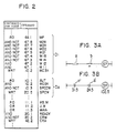
- sequence circuit is represented by a ladder diagram represented by relay symbols, as shown in Fig. 1.
- a sequence program having a logical sequence of instruction codes and operands shown in Fig. 2 is stored in a memory of the PC, thereby replacing several relays whilst still achieving proper sequence control.
- the ladder diagram shown in Fig. 1 comprises part of a ladder diagram of a numerical control (NC) machine tool system. Symbols and denote normally open and closed contacts of relays (not shown) each having a reference symbol.
- M03 spindle forward rotation instruction
- relays MF, M12 and M11 are operated to energize a relay M03X.
- a relay AUT is kept ON.
- a relay SPCCW is kept OFF
- a relay SPCW is turned on. This indicates that the spindle forward rotation instruction is supplied to a machine such as a machine tool.
- the heavy current circuit including actual relays represented by the ladder diagram controls the sequence of the machine tool.
- the PC creates a sequence program of Fig. 2 in accordance with the ladder diagram, and the sequence program is stored in a memory so as to provide sequence control.
- "RD”, "AND”, “WRT”, “OR”, “AND ⁇ NOT”, etc. in the sequence program are instruction codes, respectively. More specifically, RD is a read instruction; AND, a logical product operation instruction; WRT, a write instruction; OR, a logical sum operation instruction; and AND ⁇ NOT, an inversion/logical product instruction.
- Numeric values in the operand column represent addresses of a data memory (to be described later) incorporated in the PC.
- the addresses correspond to relay symbols (MF, M28, etc.) of Fig. 1, respectively. The relationship between the relay symbol and the address is illustrated in Fig. 1.
- the relay symbols are listed for reference at the right of the table in Fig. 2.
- the information at the addresses of the data memory which are described in the column of operands is calculated by an instruction group D1 of the sequence program.
- a logical operation MF ⁇ M28 ⁇ M24 ⁇ M22 ⁇ M21 ⁇ M18 ⁇ M14 ⁇ M12 ⁇ M11 is calculated.
- a calculation result ("1" or "0") is stored at address 10.2 of the data memory which corresponds to the relay M03X.
- the following operation is performed in accordance with an instruction group D2: AUT ⁇ M03X ⁇ SPCCW
- a calculation result is stored at address 20.5 of the data memory which is designated by the operand SPCW.
- a spindle forward rotation signal is supplied to the machine tool as an external machine, so that the spindle of the machine tool is rotated in the forward direction.
- the sequence control system having the PC is operated in accordance with the sequence program. In this control system, when an intermittent failure of the sequence occurs during automatic operation of the machine tool, it is difficult to determine the cause.
- a feed hold circuit is illustrated in Fig. 3A.
- This feed hold circuit is represented by a ladder diagram in Fig. 3B. Since the machine tool is interrupted in the feed hold state, the feed hold relay SP is stopped (de-energised). When a signal (i.e., logic level of the signal at address 102.5 of the data memory which represents the feed hold relay SP) representing the operating state of the feed hold relay SP is checked, a "1" is stored at address 102.5. The logic level "1" indicates that the feed hold relay SP should normally be in the operated (energised) state. This indicates that the failure may have been caused by the contact of the feed hold button or the pressure decrease detection switch being accidentally and temporarily opened during automatic operation.
- US-A-4 063 311 discloses a diagnostic apparatus for use with a programmable controller.
- the diagnostic apparatus operates continously in normal operation of the controller, to display information on any failure condition (i.e. disagreement between programmed and actual logic states) occurring in the current cycle of operation.
- a numerical representation of the cycle step under test is displayed on a readout for as long as the failure condition continues; or, if more than one failure occurs, each is displayed one at a time for a predetermined period. Therefore, the operator has to observe the readout carefully to note all the failures and then try to work out the underlying cause.
- JP-A-52-149580 discloses a sequence abnormality check system having features corresponding to those of the preamble of accompanying claim 1.
- a history of changes of operation states of all elements in a sequence circuit is produced continuously and automatically. There is no way to restrict attention to a particular part of a sequence circuit where a failure is known to have occurred, and consequently it is difficult for the operator to analyse the generated information in order to diagnose the failure.
- a sequence abnormality check system for a programmable controller, the programmable controller including a sequence program for controlling a machine tool in conjunction with control elements, each control element having an operational state given by a logic level of an actual signal, and having an associated address in the programmable controller; the system comprising:- first memory means for storing operational states of said elements; means for detecting changes in operational states of said elements; second memory means for storing operational states of one of said elements for which a change in operational state has been detected; and signal update writing means for writing into the second memory means an address and the new logic level of the actual operational state for each element having a changed operational state; characterised by:- address setting means for entering the addresses of elements associated with an abnormality, so as to define a set of said elements in which the abnormality has occurred; an address setting table, providing said first memory means, for storing addresses of said set of elements as defined by said address setting means and for storing the operational states of the elements corresponding to the addresses; signal update detecting means, providing said means
- An embodiment of the present invention may provide a sequence abnormality check system for a programmable controller (PC) which checks for the cause of a failure by displaying the updating of signals associated with the failure when an abnormality occurs during normal operation of the programmable controller.
- PC programmable controller
- Fig. 4 is a block diagram of a PC which employs the present invention.
- Reference numeral 1 denotes a sequence control means.
- the sequence control means 1 receives an input signal from a machine such as an NC machine tool through an input circuit 4 and a signal which is supplied from a control relay 6 in the sequence circuit and which is stored in the PC.
- the sequence control means 1 then generates an output signal to the machine through an output circuit 5 in accordance with the sequence program, thereby controlling the sequence of the machine.
- the PC of the present invention has a signal update detecting means 2, a signal update writing means 3, an address setting means 7, and a storage means.
- the storage means has an address setting table TA and a signal update storage table TB.
- the address setting means 7 sets addresses of the data memory 13(Fig.5) of the PC which store logic levels of the respective elements of the sequence circuit.
- the address setting table TA also stores the entered address and the logic level of the signal associated with this address.
- the signal update detecting means 2 compares the logic level of the signal at the address of the address setting table TA with a corresponding actual signal. In other words, the signal update detecting means 2 compares the logic levels of the signals at addresses of the data memory 13 which respectively correspond to the input circuit 4, the output circuit 5 and the control relay 6.
- the signal update writing means 3 updates the logic level at the address of the address setting table TA to that of the actual signal.
- this address, the logic level of the signal at this address, and a signal representing the last updated signal are stored in the signal update storage table TB.
- the signal update storage table TB stores an updated signal address order and the corresponding logic levels of the addresses.
- An address associated with the failure is entered at the address setting means 7 in accordance with the ladder diagram and is stored in the address setting table TA.
- the signal update detecting means 2 compares the logic level of the actual signal at the address of the address setting table TA with the logic level (upon initialization, the logic level is set at "0" or "1") corresponding to this address.
- the updated logic level is stored at the corresponding address of the signal update storage table TB.
- the logic level of the actual signal is stored in the address setting table TA.
- the signal update storage table TB stores an address order representing updating of the logic levels and the updated logic levels at the addresses.
- a signal representing the last updated signal is assigned at the last updated address.
- Fig. 5 is a block diagram of PC hardware according to the present invention.
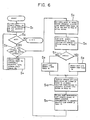
- Fig. 6 is a flow chart for explaining the operation of the PC hardware.
- reference numeral 11 denotes a ROM for storing a control program for controlling the overall operation of the PC.
- Reference numeral 12 denotes a ROM for storing a sequence program and a signal update detection program.
- Reference numeral 13 denotes a data memory comprising a RAM for storing logic levels of signals representing the respective elements of the sequence circuit which are represented by relay symbols in Figs. 1 and 3B.
- Reference numeral 10 denotes a microprocessor (MPU) for performing predetermined sequence processing in accordance with the control program and the sequence program.
- MPU microprocessor
- the MPU 10, the ROM 11 for storing the control program, the ROM 12 for storing the sequence program and the signal update detection program, and the data memory 13 for storing logic levels of signals which represent the operating states of the respective elements of the sequence circuit, constitute the sequence control means 1, the signal update detecting means 2 and the signal update writing means of Fig. 4.
- Reference numeral 14 denotes a storage hold memory for storing the address setting table TA and the signal update storage table TB; and 16, a display unit for displaying the tables TA and TB stored in the storage hold memory 14.
- the display unit 16 comprises a CRT or a printer.
- Reference numeral 15 denotes a keyboard input means used as the address setting means 7 of Fig. 4 when the address associated with the failure upon occurrence thereof is entered into the data memory.
- Reference numerals 4 and 5 denote input and output circuits for connecting the NC machine or a machine tool to the PC, respectively.
- Reference numeral 17 denotes a bus.
- the PC having the arrangement described above controls the sequence of the external machine in accordance with the sequence program stored in the ROM 12.
- Logic signals each having a predetermined logic level are stored at predetermined addresses of the data memory 13 by input and output signals from the input and output cicuits 4 and 5. The logic levels of these signals represent the operating states of the elements of the sequence circuit.
- sequence program processing (Fig. 2) is completed, the signal update detection program (Fig. 6) is executed. A cycle of the sequence program and the signal update detection program is repeated.
- the operator determines the address of a sequence element associated with the failure in accordance with the ladder diagram. This value is entered at the keyboard 15 serving as the address setting means 7, and is stored in the address setting table TA in the storage hold memory 14, as shown in Fig. 7.
- the logic level of the address signal may be entered at the address setting means 7. Otherwise, any logic level "1" or "0" is stored in the address setting table TA.
- the MPU 10 in the PC checks from the beginning of the address setting table TA whether or not the (any) address is set in the address setting table TA (S1 of Fig. 6) after one sequence control cycle is completed.
- the MPU 10 checks whether or not the signal set in the address setting table TA has the same logic level as that of the actual signal (i.e., the MPU 10 compares the logic levels of the signals which represent the operating states of the input and output circuits 4 and 5 and the control relay 6 with those which are stored in the data memory 13) (S2 and S3 of Fig. 6). If YES, the address with the next line number of the address setting table TA is subjected to comparison in the same manner as described above (S4 of Fig. 6).
- the logic level of this signal in the address setting table TA is updated to that of the corresponding actual signal (S5 of Fig. 6).
- the MPU 10 searches for a line number which stores the last updated signal in the signal update storage table TB in the storage hold memory 14; if none exists, no last updated signal is stored in the signal update storage table TB, and line number 1 is selected. When the last updated signal is present there, the next line number is selected (S6, S7, S8 and S9 of Fig. 6).
- the corresponding address and the corresponding logic level are stored in the selected line number memory location in the address setting table TB (S10 of Fig. 6).
- a signal (e.g., a mark) representing the last updated signal is stored at this memory location.
- the previously assigned mark in the table is deleted (S11 of Fig. 6).
- a line number next to the currently selected line number of the address setting table TA is selected (S4 of Fig. 6), and the same operation (S2, S3, S4, S5,... of Fig. 6) as described above will be performed.
- the MPU 10 repeatedly performs the above processing every time one sequence control cycle is completed.
- the address setting table TA stores the logic levels of current signals at the set addresses.
- the signal update storage table TB stores an address order representing updating of the signals at the addresses of the address setting table TA, and the logic levels of the current signals. Since the memory capacity of the signal update storage table TB is limited and the signal update storage table TB is used in a circulatory manner, a mark is assigned to the address storing the last updated signal in the signal update storage table TB. The mark identifies the beginning of the updated address order.
- the addresses at which the logic levels of the signals are updated, and an order of updating can be visually checked. Therefore, the operator can easily check for an address that should not have been updated (i.e. an element that should not have been operated), thereby simplifying failure check.
- the relay represented at address 31.5 Since a normally closed contact is opened when the feed hold button a is turned on once, the relay represented at address 31.5 is turned off, so that the actual signal is set at logic level "0"; the logic level of the signal stored at address 31.5 in the address setting table TA is different from that of the actual signal (S2 and S3 of Fig. 6), so that the logic level of the signal stored at address 31.5 is updated to logic level "0"; and, as shown in Fig. 8, the signal update storage table TB stores address 31.5 and logic level "1" (S5, S6, S7, S8, S10 and S11 of Fig. 6).
- the relay represented by address 31.5 When the relay represented by address 31.5 is turned off, the contact a' is opened, and the feed hold relay SP is turned off.
- the logic level of the signal stored at the actual address 102.5 becomes “0” and is different from the logic level "1" of the signal stored in the address setting table TA; the logic level of the signal in the address setting table TA is updated to "0" (S3 and S5 of Fig. 6); and, as shown in Fig. 8, address 102.5 and the corresponding logic level "0" are stored in the signal update storage.
- table TB (S6, S7, S9, S10 and (S11) of Fig. 6).
- the relay represented by address 31.5 When the feed hold button a is turned off, the relay represented by address 31.5 is turned on, and the corresponding logic level becomes "1".
- the logic level of the signal in the table TB is different from that in the address setting table TA.
- the logic level of the signal stored at address 31.5 of the address setting table TA is set to "1".
- the same address and logic level as described above are stored with line number 3 in the signal update storage table TB in Fig. 8. Since the contact of the relay represented by address 31.5 becomes ON, the feed hold relay SP is turned on.
- the logic level of the actual signal at address 102.5 becomes "1" and is different from that in the address setting table TA.
- the logic level of the signal stored at address 102.5 of the address setting table TA is updated to logic "1".
- This address 102.5 is stored as an updated address with line number 4 of the signal update storage table TB.
- the corresponding logic level "1" is also stored in the table TB.
- the last updated mark is changed from line number 3 to line number 4 of the signal update storage table TB (It should be noted that the mark has not been described in the preceding part of the specification, but that the mark has been actually relabeled from line number 1 to line number 2, line number 2 to line number 3 and line number 3 to line number 4 of the signal update storage table TB).
- the logic levels of the signals from the input and output circuits are stored in the data memory.
- the signals from the input and output signals need not be stored in the data memory. Addresses are assigned to the respective terminals of the input and output circuits.
- the logic levels of the signals may be read out from the data memory for storing the signals having logic levels representing the operating states of the terminals of the input and output circuits and the control relay in response to the address entered at the address setting means.
Landscapes
- Physics & Mathematics (AREA)
- General Physics & Mathematics (AREA)
- Engineering & Computer Science (AREA)
- Automation & Control Theory (AREA)
- Programmable Controllers (AREA)
- Testing And Monitoring For Control Systems (AREA)
Claims (4)
- Kontroll-System zur Erfassung von Sequenzabnormitäten für einen programmierbaren Kontroller, wobei der programmierbare Kontroller ein Sequenzprogramm zum Steuern einer Werkzeugmaschine in Zusammenwirkung mit Steuer-Elementen enthält und wobei jedes Steuer-Element einen Betriebszustand aufweist, der durch einen logischen Pegel eines wirksamen Signals gegeben ist, und eine ihm zugeordnete Adresse in dem programmierbaren Kontroller hat, welches System umfaßt:
ein erstes Speichermittel zum Speichern von Betriebszuständen der Elemente,
ein Mittel zum Erfassen von Änderungen von Betriebszuständen der Elemente,
ein zweites Speichermittel zum Speichern von Betriebszuständen eines der Elemente, für das eine Änderung eines Betriebszustands erfaßt worden ist, und
ein Signalaktualisierungs-Einschreibmittel zum Einschreiben einer Adresse und des neuen logischen Pegels des aktuellen Betriebszustands für jedes Element, das einen geänderten Betriebszustand aufweist, in das zweite Speichermittel,
gekennzeichnet durch
ein Adresseneinstell-Mittel (7) zum Eingehen der Adressen von Elementen, denen eine Abnormität zuzuordnen ist, um auf diese Weise einen Satz von Elementen zu definieren, in denen die Abnormität aufgetreten ist,
eine Adresseneinstell-Tabelle (TA), die das erste Speichermittel voraussetzt, zum Speichern von Adressen des Satzes von Elementen, wie sie durch das Adresseneinstell-Mittel (7) definiert sind, und zum Speichern der Betriebszustände der Elemente, die den Adressen entsprechen,
ein Signalaktualisierungs-Mittel (2), das das Mittel zum Erfassen von Änderungen der Betriebszustände der Elemente voraussetzt und das auf die gespeicherten Inhalte der Adresseneinstell-Tabelle (TA) reagiert, zum Erzeugen eines Ausgangssignals, falls ein Betriebszustand eines Elements, der in der Adresseneinstell-Tabelle (TA) gespeichert ist, von dem logischen Pegel des wirksamen Signals für dieses Element unterschiedlich ist, wenn das Sequenzprogramm folgend auf das Einstellen der Adresse dieses Elements in der Adresseneinstell-Tabelle (TA) durch das Adresseneinstell-Mittel (7) abgearbeitet wird, und
eine Signalaktualisierungs-Speichertabelle (TB), die das zweite Speichermittel voraussetzt, und
ferner dadurch gekennzeichnet,
daß das Signalaktualisierungs-Einschreibmittel (3) betreibbar ist, um in die Signalaktualisierungs-Speichertabelle (TB) ein Zeichen einzuschreiben, das diejenige Adresse kennzeichnet, die zuletzt aktualisiert wurde, und das zum Aktualisieren der Betriebszustände dient, die in der Adresseneinstell-Tabelle (TA) gespeichert sind, um diese den logischen Pegeln der wirksamen Signale entsprechen zu lassen, und
daß ein Anzeigemittel (16) in Reaktion auf die Adressen eines Satzes von Elementen, die in der Adresseneinstell-Tabelle (TA) gespeichert sind, betreibbar ist, um in Aufeinanderfolge die Adressen, welche in der Signalaktualisierungs-Speichertabelle (TB) gespeichert sind, zusammen mit den entsprechenden logischen Pegeln und dem Zeichen, das die zuletzt aktualisierte Adresse kennzeichnet, anzuzeigen, um dadurch das Erkennen des Elements zu erleichtern, das die Abnormität verursacht hat. - System nach Anspruch 1, das ferner einen Speicher (13) enthält und bei dem die Adresse, welche durch das Adresseneinstell-Mittel (7) erzeugt ist, eine Speicheradresse des Speichers (13) zum Speichern des Betriebszustands des Elements, das der Adresse entspricht, umfaßt.
- System nach Anspruch 1, das ferner einen Speicher (13), Eingangs- (4) und Ausgangsschaltungen (5) enthält und bei dem die Adresse, die durch das Adresseneinstell-Mittel (7) erzeugt ist, Speicheradressen des Speichers (13) zum Speichern des Betriebszustands der Steuer-Elemente und von Signalen, die einem Zustand der Eingangs- und Ausgangsschaltungen (4, 5) entsprechen, umfaßt.
- System nach einem der vorhergehenden Ansprüche, wobei das System wiederholt in einem Zyklus zusammen mit einer Sequenzsteuerung betreibbar ist.
Applications Claiming Priority (2)
| Application Number | Priority Date | Filing Date | Title |
|---|---|---|---|
| JP79354/83 | 1983-05-09 | ||
| JP58079354A JPS59205614A (ja) | 1983-05-09 | 1983-05-09 | プログラマブルコントロ−ラにおけるシ−ケンス異常チエツク方式 |
Publications (3)
| Publication Number | Publication Date |
|---|---|
| EP0148951A1 EP0148951A1 (de) | 1985-07-24 |
| EP0148951A4 EP0148951A4 (de) | 1987-07-27 |
| EP0148951B1 true EP0148951B1 (de) | 1992-01-15 |
Family
ID=13687562
Family Applications (1)
| Application Number | Title | Priority Date | Filing Date |
|---|---|---|---|
| EP84901808A Expired EP0148951B1 (de) | 1983-05-09 | 1984-05-04 | System zum kontrollieren von abnormalitäten in programmierbarem kontroller |
Country Status (5)
| Country | Link |
|---|---|
| US (1) | US4633384A (de) |
| EP (1) | EP0148951B1 (de) |
| JP (1) | JPS59205614A (de) |
| DE (1) | DE3485459D1 (de) |
| WO (1) | WO1984004610A1 (de) |
Families Citing this family (11)
| Publication number | Priority date | Publication date | Assignee | Title |
|---|---|---|---|---|
| JPH0670764B2 (ja) * | 1985-03-06 | 1994-09-07 | 株式会社日立製作所 | シ−ケンス制御装置 |
| US4851985A (en) * | 1985-04-15 | 1989-07-25 | Logitek, Inc. | Fault diagnosis system for comparing counts of commanded operating state changes to counts of actual resultant changes |
| US5133066A (en) * | 1985-10-24 | 1992-07-21 | International Business Machines Corporation | Method for selecting multiple versions of data in a reduced record units text editing system |
| JPS62243008A (ja) * | 1986-04-15 | 1987-10-23 | Fanuc Ltd | Pmcの信号トレ−ス制御方式 |
| GB2200476B (en) * | 1987-01-29 | 1991-02-06 | British Gas Plc | Monitor system |
| JPH0677216B2 (ja) * | 1987-05-25 | 1994-09-28 | マツダ株式会社 | シ−ケンスプログラム制御系のモニタ装置 |
| JPH04284511A (ja) * | 1991-03-14 | 1992-10-09 | Toyota Motor Corp | プログラマブルコントローラ異常検出装置 |
| JP2792772B2 (ja) * | 1991-04-01 | 1998-09-03 | 三菱電機株式会社 | プログラマブルコントローラ及びそのシーケンスプログラムモニタ方法 |
| WO1993018441A1 (en) * | 1992-03-09 | 1993-09-16 | Electronic Data Systems Corporation | Method and system for automatic graphic display modification based on control program modification |
| US5870693A (en) * | 1996-03-01 | 1999-02-09 | Sony Display Device (Singapore) Pte. Ltd. | Apparatus and method for diagnosis of abnormality in processing equipment |
| US7419467B2 (en) * | 1998-11-25 | 2008-09-02 | M3 Electronics, Inc. | Medical inspection device |
Family Cites Families (9)
| Publication number | Priority date | Publication date | Assignee | Title |
|---|---|---|---|---|
| JPS5332030B2 (de) * | 1972-01-18 | 1978-09-06 | ||
| JPS5518362B2 (de) * | 1974-10-21 | 1980-05-19 | ||
| US3997879A (en) * | 1975-12-24 | 1976-12-14 | Allen-Bradley Company | Fault processor for programmable controller with remote I/O interface racks |
| US4062061A (en) * | 1976-04-15 | 1977-12-06 | Xerox Corporation | Error log for electrostatographic machines |
| JPS52149580A (en) * | 1976-06-08 | 1977-12-12 | Kyosan Electric Mfg Co Ltd | Record memorizing method |
| US4063311A (en) * | 1976-08-17 | 1977-12-13 | Cincinnati Milacron Inc. | Asynchronously operating signal diagnostic system for a programmable machine function controller |
| JPS5760412A (en) * | 1980-09-29 | 1982-04-12 | Omron Tateisi Electronics Co | Monitoring method of programmable logic controller of random acess discrete address diagram system |
| JPS57206923A (en) * | 1981-06-15 | 1982-12-18 | Hitachi Ltd | External trouble diagnosing device for process controller |
| DE3206891A1 (de) * | 1982-02-26 | 1983-09-15 | Robert Bosch Gmbh, 7000 Stuttgart | Verfahren zur fehlerdiagnose fuer speicherprogrammierbare steuerungen |
-
1983
- 1983-05-09 JP JP58079354A patent/JPS59205614A/ja active Pending
-
1984
- 1984-05-04 EP EP84901808A patent/EP0148951B1/de not_active Expired
- 1984-05-04 WO PCT/JP1984/000227 patent/WO1984004610A1/ja active IP Right Grant
- 1984-05-04 US US06/695,362 patent/US4633384A/en not_active Expired - Fee Related
- 1984-05-04 DE DE8484901808T patent/DE3485459D1/de not_active Expired - Lifetime
Also Published As
| Publication number | Publication date |
|---|---|
| DE3485459D1 (de) | 1992-02-27 |
| WO1984004610A1 (en) | 1984-11-22 |
| EP0148951A4 (de) | 1987-07-27 |
| US4633384A (en) | 1986-12-30 |
| JPS59205614A (ja) | 1984-11-21 |
| EP0148951A1 (de) | 1985-07-24 |
Similar Documents
| Publication | Publication Date | Title |
|---|---|---|
| EP0148951B1 (de) | System zum kontrollieren von abnormalitäten in programmierbarem kontroller | |
| US5469352A (en) | Operation history display device of numerical control apparatus | |
| US4616307A (en) | Programmable controller alarm display method | |
| JPH03154847A (ja) | 故障診断装置 | |
| EP0436035B1 (de) | Verfahren zur Anzeige der Betriebsgeschichte einer Maschine | |
| JPH03137518A (ja) | 故障診断装置 | |
| JPS60262204A (ja) | プログラマブル・コントロ−ラ | |
| JP2608593B2 (ja) | 故障診断方法 | |
| JPS60122407A (ja) | プログラマブル・コントロ−ラ | |
| US4887220A (en) | Parameter initializing method for a programmable machine controller | |
| US4498130A (en) | Apparatus for remotely operating output terminals of a copying machine or the like during self-diagnosis | |
| JPH0573125A (ja) | Nc工作機械の加工監視方式 | |
| JPS633925A (ja) | アラ−ム内容印字機能付き射出成形機 | |
| JPS63240602A (ja) | シ−ケンスコントロ−ラの異常診断装置 | |
| JPH06327862A (ja) | 自動制御ミシンにおける故障箇所検出装置 | |
| JPH0152762B2 (de) | ||
| JPS5934549A (ja) | 複写機用制御装置 | |
| JPS61813A (ja) | シ−ケンス制御装置の故障個所判定方式 | |
| JP2788461B2 (ja) | 加工機械の状態検出装置 | |
| JPS6155702A (ja) | 数値制御装置 | |
| JPH02176805A (ja) | 入出力制御に関する故障診断装置 | |
| JPS5934550A (ja) | 複写機用制御装置 | |
| KR100238663B1 (ko) | 이형로보트시스템의 자기 진단 방법 | |
| JPS58219615A (ja) | プログラマブルコントロ−ラ | |
| JPS5916014A (ja) | シ−ケンスコントロ−ラにおける異常チエツク方式 |
Legal Events
| Date | Code | Title | Description |
|---|---|---|---|
| PUAI | Public reference made under article 153(3) epc to a published international application that has entered the european phase |
Free format text: ORIGINAL CODE: 0009012 |
|
| 17P | Request for examination filed |
Effective date: 19850123 |
|
| AK | Designated contracting states |
Designated state(s): DE FR GB |
|
| A4 | Supplementary search report drawn up and despatched |
Effective date: 19870727 |
|
| 17Q | First examination report despatched |
Effective date: 19890131 |
|
| RBV | Designated contracting states (corrected) |
Designated state(s): DE |
|
| GRAA | (expected) grant |
Free format text: ORIGINAL CODE: 0009210 |
|
| AK | Designated contracting states |
Kind code of ref document: B1 Designated state(s): DE |
|
| REF | Corresponds to: |
Ref document number: 3485459 Country of ref document: DE Date of ref document: 19920227 |
|
| PLBE | No opposition filed within time limit |
Free format text: ORIGINAL CODE: 0009261 |
|
| STAA | Information on the status of an ep patent application or granted ep patent |
Free format text: STATUS: NO OPPOSITION FILED WITHIN TIME LIMIT |
|
| 26N | No opposition filed | ||
| PG25 | Lapsed in a contracting state [announced via postgrant information from national office to epo] |
Ref country code: DE Effective date: 19930202 |