EP0146233B1 - Low temperature process for annealing shallow implanted n+/p junctions - Google Patents
Low temperature process for annealing shallow implanted n+/p junctions Download PDFInfo
- Publication number
- EP0146233B1 EP0146233B1 EP84307173A EP84307173A EP0146233B1 EP 0146233 B1 EP0146233 B1 EP 0146233B1 EP 84307173 A EP84307173 A EP 84307173A EP 84307173 A EP84307173 A EP 84307173A EP 0146233 B1 EP0146233 B1 EP 0146233B1
- Authority
- EP
- European Patent Office
- Prior art keywords
- annealing
- implanted
- silicon
- semiconductor
- implantation
- Prior art date
- Legal status (The legal status is an assumption and is not a legal conclusion. Google has not performed a legal analysis and makes no representation as to the accuracy of the status listed.)
- Expired
Links
Images

Classifications
-
- H—ELECTRICITY
- H10—SEMICONDUCTOR DEVICES; ELECTRIC SOLID-STATE DEVICES NOT OTHERWISE PROVIDED FOR
- H10P—GENERIC PROCESSES OR APPARATUS FOR THE MANUFACTURE OR TREATMENT OF DEVICES COVERED BY CLASS H10
- H10P30/00—Ion implantation into wafers, substrates or parts of devices
- H10P30/20—Ion implantation into wafers, substrates or parts of devices into semiconductor materials, e.g. for doping
- H10P30/202—Ion implantation into wafers, substrates or parts of devices into semiconductor materials, e.g. for doping characterised by the semiconductor materials
- H10P30/204—Ion implantation into wafers, substrates or parts of devices into semiconductor materials, e.g. for doping characterised by the semiconductor materials into Group IV semiconductors
-
- H—ELECTRICITY
- H10—SEMICONDUCTOR DEVICES; ELECTRIC SOLID-STATE DEVICES NOT OTHERWISE PROVIDED FOR
- H10P—GENERIC PROCESSES OR APPARATUS FOR THE MANUFACTURE OR TREATMENT OF DEVICES COVERED BY CLASS H10
- H10P30/00—Ion implantation into wafers, substrates or parts of devices
- H10P30/20—Ion implantation into wafers, substrates or parts of devices into semiconductor materials, e.g. for doping
- H10P30/208—Ion implantation into wafers, substrates or parts of devices into semiconductor materials, e.g. for doping of electrically inactive species
-
- H—ELECTRICITY
- H10—SEMICONDUCTOR DEVICES; ELECTRIC SOLID-STATE DEVICES NOT OTHERWISE PROVIDED FOR
- H10P—GENERIC PROCESSES OR APPARATUS FOR THE MANUFACTURE OR TREATMENT OF DEVICES COVERED BY CLASS H10
- H10P30/00—Ion implantation into wafers, substrates or parts of devices
- H10P30/20—Ion implantation into wafers, substrates or parts of devices into semiconductor materials, e.g. for doping
- H10P30/21—Ion implantation into wafers, substrates or parts of devices into semiconductor materials, e.g. for doping of electrically active species
-
- H—ELECTRICITY
- H10—SEMICONDUCTOR DEVICES; ELECTRIC SOLID-STATE DEVICES NOT OTHERWISE PROVIDED FOR
- H10P—GENERIC PROCESSES OR APPARATUS FOR THE MANUFACTURE OR TREATMENT OF DEVICES COVERED BY CLASS H10
- H10P30/00—Ion implantation into wafers, substrates or parts of devices
- H10P30/20—Ion implantation into wafers, substrates or parts of devices into semiconductor materials, e.g. for doping
- H10P30/28—Ion implantation into wafers, substrates or parts of devices into semiconductor materials, e.g. for doping characterised by an annealing step, e.g. for activation of dopants
-
- H—ELECTRICITY
- H10—SEMICONDUCTOR DEVICES; ELECTRIC SOLID-STATE DEVICES NOT OTHERWISE PROVIDED FOR
- H10P—GENERIC PROCESSES OR APPARATUS FOR THE MANUFACTURE OR TREATMENT OF DEVICES COVERED BY CLASS H10
- H10P95/00—Generic processes or apparatus for manufacture or treatments not covered by the other groups of this subclass
- H10P95/94—Hydrogenation or deuterisation, e.g. using atomic hydrogen from a plasma
Definitions
- the invention relates generally to production of semiconductors and, more specifically, low temperature produced semiconductors.
- Ion implantation has become a powerful VLSI tool for the formation of heavily doped shallow junctions.
- ion implantation is generally followed by greater than 850° thermal anneal to remove the implantation damage and activate the dopants.
- Such high temperature anneal is not desirable and may be unacceptable for very shallow junctions ( ⁇ 0.1 pm).
- implantation of phosphorus and arsenic at high dose levels severely damages the crystal lattice and subsequently is difficult to anneal even at high temperatures (900°C). This tends to make the implanted junctions more leaky resulting in lower breakdown voltages. Therefore it is necessary to develop methods for completely annealing implantation damage preferably at low temperatures.
- localized beam annealing which includes laser and electron beam annealing and rapid thermal annealing (RTA) which herein will be taken to include processes employing pulsed incoherent lamp sources or graphite strip heating.
- RTA rapid thermal annealing
- the beam, laser or electron is directed on a very small region at the surface rapidly bringing the silicon temperature up to a point where epitaxial regrowth can result.
- the rapid localized heating and melting and cooling and solidification involved can result in imperfections in the lattice and can give rise to electrically active defects.
- Rapid thermal anneals employing pulsed incoherent light sources for annealing ion implantation damage typically use pulse durations of the order of a few hundredmicroseconds with incident energies in a range of 20 to 30 joules/cm 2 . This approach can be used for the uniform annealing and dopant activation of large areas. Rapid thermal anneals using graphite strip heaters are equally effective. However, it has been shown that RTA at least for the case of graphite strip heaters produces annealed implanted layers that degrade under simulated subsequent low temperature processing. Both RTA approaches uniformly heat the damaged silicon layer. However, both bring the temperature of the whole silicon surface to the 1000 to 1200°C range and consequently neither is a true low temperature process.
- Hydrogen is generally believed to bond chemically to any dangling bonds in the silicon and in the energy band picture to move localized states in the band gap to the band edges.
- Successful demonstration of the reduction of bulk recombination centers in ribbon silicon using hydrogen ions as a passivant has been shown by Seager.
- Laser beam damage silicon exposed to a hydrogen plasma for four hours experienced a total passivation of residual pointdefe ⁇ ts.
- hydrogen is believed to be responsible for the low surface state density seen in MOS capacitor structures after a low temperature post metalization hydrogen anneal.
- the invention resides broadly in a method of producing a silicon semiconductor that has been doped by ion implantation with an element selected from the group consisting of arsenic and phosphorus by low temperature annealing said silicon semiconductor, said method comprising: ion beam implantation of hydrogen ions subsequent to and in the same area as the element selected from the above group that has been implanted, and subsequently annealing the semiconductor at a temperature between about 500°C and about 600°C for a time of about one hour in an inert atmosphere.
- hydrogen ions are implanted after the dopant implantation followed by a low temperature annealing in nitrogen.
- a Kaufman ion source is used for H + implantation which allows large dosages to be implanted in a very short time.
- the implantation damage is extensive enough to help the dopant activation at low temperature annealing.
- the presence of hydrogen ions in the lattice passivates the defects which usually require high temperature anneal and in some instances are not thermally annealable.
- a net result is a low leakage shallow junction device fabricated at about 500°C.
- the preferred method of practicing this invention uses a low energy hydrogen ion beam to passivate the defects result from the implantation of an n + region into p-type silicon and uses a low temperature furnace anneal to activate the dopants.
- the n + /p junctions employed were made by implanting 70 to 75 KeV As+ ions into p-type boron doped silicon which had channel stops present. The dosage was 5 X 10 15 arsenic atoms/cm 2 and the implanted area was 3.7x10- 2 cm 2 .
- Using a Kaufman type ion source 0.4 KeV H + ions were implanted into the above structure for one minute.
- the hydrogen ion beam had an extractor voltage of 0.3 KeV and an accelerator current of 200 mA.
- the silicon samples were then annealed at 500°C or 600°C for one hour in nitrogen or argon ambience.
- Spreading resistance measurements were subsequently made to examine the dopant profile and the degree of dopant activation.
- Current-voltage (I - V) measurements were made at different temperatures to examine the diode characteristics and transport mechanisms.
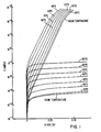
- Figure 1 shows repesentative I-V-T characteristics for diode structures annealed at 500°C after the low energy hydrogen ion implantation.
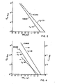
- Figure 3 shows I-V-T for diode structures that underwent a 600°C one hour anneal in N 2 after a low energy hydrogen implant.
- Figure 4 shows the activation plots obtained from the forward and reverse current measurements. The activation energy from the forward bias was measured to be 1.04 eV. The plot of I versus 1000/T for the reverse current however, shows two activation energies: 0.69 eV for temperatures near room temperature and 0.99 eV for temperatures above 50°C.
- the activation energy of 0.99 eV in reverse bias for T 2: 50°C suggests the dominance of diffusion-recombination current even in reverse bias at higher temperatures. That is, the generation-recombination current is now smaller even in reverse bias than the diffusion-recombination current for temperatures greater than or equal to 50°C.
- the lower activation energy in reverse bias is suggestive of a generation recombination current indicating that some electrically active defects are still present even in the 600°C annealed diodes. While it is not possible to passivate all the defects, a regime is approached where the generation-recombination component of the current is comparable to the diffusion-recombination current component even in reverse bias.
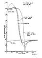
- FIG. 5 The results of spreading resistance measurements are shown in Figure 5. Also shown in the Figures is a spreading resistance plot for a diode that did not have any H + implant but was annealed at 550°C for 75 minutes and then at 900°C for 30 minutes. Also shown is the As implanted profile derived by theory. The junction depth after a 600°C one hour anneal shows very little dopant redistribution. The dopant concentration is measured from spreading resistance shows that most of the implanted As has been activated.
- Low energy hydrogen ion implantation may also be used to improve the performance of dendritic web photovoltaic cells.
- Cells fabricated on dendritic web silicon in n + /p/p + structure give device efficiencies as high as 15% under standard illumination conditions of air mass one (AM1) with an average device efficiency of about 13% in AM1. This compares favorably with cells fabricated on float zone silicon which is a single crystal using the same process where efficiencies of between 14 and 15% were obtained in AM1.
- the use of hydrogen ion beam passivation dramatically improves those web cells in the tail of the efficiency distribution.
- the result of using hydrogen ion beam passivation is a much tighter distribution of cell efficiencies.
- Table 1 provides a summary of the experimental verification of the invention. It is shown that 70 KeV, 4x10 15 cm -2 arsenic implantation followed by 550°C for 75 minutes and 900°C for 30 minutes thermal anneal in nitrogen is not sufficient to produce low leakage junctions. Leakage current in these devices of the order of 10 4 na/cm l which is about 3 to 4 orders of magnitude higher than a desirable value.
- Table 1 also shows that if we take the 550°C for 75 minutes and 900°C for 30 minutes N 2 anneal devices with no contact metal and implant 0.4 KeV hydrogen ions with a current density -10- 3 amps/cm 2 from a Kaufman ion source, then leakage can be reduced to 10 3 na/cm 2 from 10 4 na/cm 2 .
- Device 3 which received straight 500°C for one hour heat treatment after arsenic implantation without the hydrogen ions showed a leakage current of 5x10 4 na/cm 2 but nearly complete dopant activation at the surface within a factor of 2. This indicates the 500°C for one hour heat treatment helps the dopant activation but is not sufficient to reduce the leakage current. Hydrogen ions are needed to provide the defect passivation and lower the leakage current from 5 ⁇ 10 4 na/cm 2 to 10 2 na/cm: '
- Table 2 shows an example of the improvement that can be seen in dendritic web photovoltaic cells in the tail of an efficiency distribution when low energy hydrogen ion beam implantation is used to reduce the number of bulk recombination centers in the web silicon photovoltaic cell.
- Low energy hydrogen ion implantation with low temperature annealing offers an alternative to other processes used for annealing out implantation damage and to activate dopants in implanted silicon.
- Low energy hydrogen ion implantation and low temperature annealing processing for damage passivation and dopant activation not only provides results comparable to other annealing processes but also allows the passivation of electrically active residual defects an advantage not offered by other techniques.
- furnace anneals were used to activate the dopants the process is not limited to this because low energy hydrogen ion implants can be used in conjunction with lower temperature RTA approaches reducing the processing time involved. When used with broad beam ion sources this process can be adapted to the fabrication of extremely shallow junctions used in VLSI as well as dendritic web photovoltaic cells.
Landscapes
- Photovoltaic Devices (AREA)
- Bipolar Transistors (AREA)
Applications Claiming Priority (2)
| Application Number | Priority Date | Filing Date | Title |
|---|---|---|---|
| US543745 | 1983-10-20 | ||
| US06/543,745 US4522657A (en) | 1983-10-20 | 1983-10-20 | Low temperature process for annealing shallow implanted N+/P junctions |
Publications (2)
| Publication Number | Publication Date |
|---|---|
| EP0146233A1 EP0146233A1 (en) | 1985-06-26 |
| EP0146233B1 true EP0146233B1 (en) | 1988-06-01 |
Family
ID=24169404
Family Applications (1)
| Application Number | Title | Priority Date | Filing Date |
|---|---|---|---|
| EP84307173A Expired EP0146233B1 (en) | 1983-10-20 | 1984-10-18 | Low temperature process for annealing shallow implanted n+/p junctions |
Country Status (6)
| Country | Link |
|---|---|
| US (1) | US4522657A (cg-RX-API-DMAC7.html) |
| EP (1) | EP0146233B1 (cg-RX-API-DMAC7.html) |
| JP (1) | JPS60102732A (cg-RX-API-DMAC7.html) |
| AU (1) | AU567190B2 (cg-RX-API-DMAC7.html) |
| DE (1) | DE3471826D1 (cg-RX-API-DMAC7.html) |
| ES (1) | ES8602300A1 (cg-RX-API-DMAC7.html) |
Families Citing this family (252)
| Publication number | Priority date | Publication date | Assignee | Title |
|---|---|---|---|---|
| US4610731A (en) * | 1985-04-03 | 1986-09-09 | At&T Bell Laboratories | Shallow impurity neutralization |
| JP2516951B2 (ja) * | 1987-02-06 | 1996-07-24 | 松下電器産業株式会社 | 半導体装置の製造方法 |
| US5453153A (en) * | 1987-11-13 | 1995-09-26 | Kopin Corporation | Zone-melting recrystallization process |
| US5021119A (en) * | 1987-11-13 | 1991-06-04 | Kopin Corporation | Zone-melting recrystallization process |
| US5079187A (en) * | 1987-12-07 | 1992-01-07 | The Regents Of The University Of California | Method for processing semiconductor materials |
| US5048163A (en) * | 1987-12-07 | 1991-09-17 | Asmus John F | System for processing semiconductor materials |
| US4912062A (en) * | 1988-05-20 | 1990-03-27 | Motorola, Inc. | Method of eliminating bird's beaks when forming field oxide without nitride mask |
| US5023458A (en) * | 1989-01-04 | 1991-06-11 | Eaton Corporation | Ion beam control system |
| US4914305A (en) * | 1989-01-04 | 1990-04-03 | Eaton Corporation | Uniform cross section ion beam system |
| ATE127651T1 (de) * | 1989-05-04 | 1995-09-15 | Univ California | Vorrichtung und verfahren zur behandlung von materialien. |
| US5198881A (en) * | 1989-12-28 | 1993-03-30 | Massachusetts Institute Of Technology | Barrier layer device processing |
| EP0717437B1 (en) * | 1994-12-12 | 2002-04-24 | Advanced Micro Devices, Inc. | Method of forming buried oxide layers |
| JPH10209168A (ja) * | 1997-01-24 | 1998-08-07 | Nec Corp | 半導体装置の製造方法 |
| JP3123465B2 (ja) * | 1997-06-09 | 2001-01-09 | 日本電気株式会社 | Misトランジスタの製造方法 |
| JP3450163B2 (ja) | 1997-09-12 | 2003-09-22 | Necエレクトロニクス株式会社 | 半導体装置の製造方法 |
| US6319784B1 (en) | 1999-05-26 | 2001-11-20 | Taiwan Semiconductor Manufacturing Company | Using high temperature H2 anneal to recrystallize S/D and remove native oxide simultaneously |
| WO2002045871A1 (en) * | 2000-12-06 | 2002-06-13 | Angstron Systems, Inc. | System and method for modulated ion-induced atomic layer deposition (mii-ald) |
| US7026229B2 (en) * | 2001-11-28 | 2006-04-11 | Vartan Semiconductor Equipment Associates, Inc. | Athermal annealing with rapid thermal annealing system and method |
| DE10260644B3 (de) * | 2002-12-23 | 2004-03-18 | Infineon Technologies Ag | Verfahren zum Dotieren eines Halbleiterkörpers |
| DE102005063462B4 (de) * | 2004-09-22 | 2017-10-12 | Infineon Technologies Ag | Verfahren zur Herstellung einer dotierten Zone in einem Halbleiterkörper |
| EP2004553A1 (en) * | 2006-04-07 | 2008-12-24 | Institute Of Geological And Nuclear Sciences Limited | Zinc oxide materials and methods for their preparation |
| EP2319087A1 (en) | 2008-06-11 | 2011-05-11 | Solar Implant Technologies Inc. | Solar cell fabrication with faceting and ion implantation |
| US8373439B2 (en) | 2009-04-14 | 2013-02-12 | Monolithic 3D Inc. | 3D semiconductor device |
| US9711407B2 (en) | 2009-04-14 | 2017-07-18 | Monolithic 3D Inc. | Method of manufacturing a three dimensional integrated circuit by transfer of a mono-crystalline layer |
| US8754533B2 (en) | 2009-04-14 | 2014-06-17 | Monolithic 3D Inc. | Monolithic three-dimensional semiconductor device and structure |
| US8405420B2 (en) | 2009-04-14 | 2013-03-26 | Monolithic 3D Inc. | System comprising a semiconductor device and structure |
| US8378715B2 (en) | 2009-04-14 | 2013-02-19 | Monolithic 3D Inc. | Method to construct systems |
| US8395191B2 (en) | 2009-10-12 | 2013-03-12 | Monolithic 3D Inc. | Semiconductor device and structure |
| US8362800B2 (en) | 2010-10-13 | 2013-01-29 | Monolithic 3D Inc. | 3D semiconductor device including field repairable logics |
| US8362482B2 (en) | 2009-04-14 | 2013-01-29 | Monolithic 3D Inc. | Semiconductor device and structure |
| US8384426B2 (en) | 2009-04-14 | 2013-02-26 | Monolithic 3D Inc. | Semiconductor device and structure |
| US7986042B2 (en) | 2009-04-14 | 2011-07-26 | Monolithic 3D Inc. | Method for fabrication of a semiconductor device and structure |
| US8669778B1 (en) | 2009-04-14 | 2014-03-11 | Monolithic 3D Inc. | Method for design and manufacturing of a 3D semiconductor device |
| US8258810B2 (en) | 2010-09-30 | 2012-09-04 | Monolithic 3D Inc. | 3D semiconductor device |
| US9577642B2 (en) | 2009-04-14 | 2017-02-21 | Monolithic 3D Inc. | Method to form a 3D semiconductor device |
| US8427200B2 (en) | 2009-04-14 | 2013-04-23 | Monolithic 3D Inc. | 3D semiconductor device |
| US8058137B1 (en) | 2009-04-14 | 2011-11-15 | Monolithic 3D Inc. | Method for fabrication of a semiconductor device and structure |
| US9509313B2 (en) | 2009-04-14 | 2016-11-29 | Monolithic 3D Inc. | 3D semiconductor device |
| US8749053B2 (en) | 2009-06-23 | 2014-06-10 | Intevac, Inc. | Plasma grid implant system for use in solar cell fabrications |
| US8148237B2 (en) | 2009-08-07 | 2012-04-03 | Varian Semiconductor Equipment Associates, Inc. | Pressurized treatment of substrates to enhance cleaving process |
| US10043781B2 (en) | 2009-10-12 | 2018-08-07 | Monolithic 3D Inc. | 3D semiconductor device and structure |
| US10157909B2 (en) | 2009-10-12 | 2018-12-18 | Monolithic 3D Inc. | 3D semiconductor device and structure |
| US11984445B2 (en) | 2009-10-12 | 2024-05-14 | Monolithic 3D Inc. | 3D semiconductor devices and structures with metal layers |
| US10366970B2 (en) | 2009-10-12 | 2019-07-30 | Monolithic 3D Inc. | 3D semiconductor device and structure |
| US8581349B1 (en) | 2011-05-02 | 2013-11-12 | Monolithic 3D Inc. | 3D memory semiconductor device and structure |
| US12027518B1 (en) | 2009-10-12 | 2024-07-02 | Monolithic 3D Inc. | 3D semiconductor devices and structures with metal layers |
| US10910364B2 (en) | 2009-10-12 | 2021-02-02 | Monolitaic 3D Inc. | 3D semiconductor device |
| US8476145B2 (en) | 2010-10-13 | 2013-07-02 | Monolithic 3D Inc. | Method of fabricating a semiconductor device and structure |
| US10388863B2 (en) | 2009-10-12 | 2019-08-20 | Monolithic 3D Inc. | 3D memory device and structure |
| US9099424B1 (en) | 2012-08-10 | 2015-08-04 | Monolithic 3D Inc. | Semiconductor system, device and structure with heat removal |
| US11018133B2 (en) | 2009-10-12 | 2021-05-25 | Monolithic 3D Inc. | 3D integrated circuit |
| US10354995B2 (en) | 2009-10-12 | 2019-07-16 | Monolithic 3D Inc. | Semiconductor memory device and structure |
| US8536023B2 (en) | 2010-11-22 | 2013-09-17 | Monolithic 3D Inc. | Method of manufacturing a semiconductor device and structure |
| US8450804B2 (en) | 2011-03-06 | 2013-05-28 | Monolithic 3D Inc. | Semiconductor device and structure for heat removal |
| US8148728B2 (en) | 2009-10-12 | 2012-04-03 | Monolithic 3D, Inc. | Method for fabrication of a semiconductor device and structure |
| US11374118B2 (en) | 2009-10-12 | 2022-06-28 | Monolithic 3D Inc. | Method to form a 3D integrated circuit |
| US8742476B1 (en) | 2012-11-27 | 2014-06-03 | Monolithic 3D Inc. | Semiconductor device and structure |
| EP2814051A1 (en) * | 2010-02-09 | 2014-12-17 | Intevac, Inc. | Shadow mask implantation system |
| US8541819B1 (en) | 2010-12-09 | 2013-09-24 | Monolithic 3D Inc. | Semiconductor device and structure |
| US8298875B1 (en) | 2011-03-06 | 2012-10-30 | Monolithic 3D Inc. | Method for fabrication of a semiconductor device and structure |
| US9099526B2 (en) | 2010-02-16 | 2015-08-04 | Monolithic 3D Inc. | Integrated circuit device and structure |
| US8026521B1 (en) | 2010-10-11 | 2011-09-27 | Monolithic 3D Inc. | Semiconductor device and structure |
| US8492886B2 (en) | 2010-02-16 | 2013-07-23 | Monolithic 3D Inc | 3D integrated circuit with logic |
| US8461035B1 (en) | 2010-09-30 | 2013-06-11 | Monolithic 3D Inc. | Method for fabrication of a semiconductor device and structure |
| US8373230B1 (en) | 2010-10-13 | 2013-02-12 | Monolithic 3D Inc. | Method for fabrication of a semiconductor device and structure |
| US9219005B2 (en) | 2011-06-28 | 2015-12-22 | Monolithic 3D Inc. | Semiconductor system and device |
| US9953925B2 (en) | 2011-06-28 | 2018-04-24 | Monolithic 3D Inc. | Semiconductor system and device |
| US10217667B2 (en) | 2011-06-28 | 2019-02-26 | Monolithic 3D Inc. | 3D semiconductor device, fabrication method and system |
| US8642416B2 (en) | 2010-07-30 | 2014-02-04 | Monolithic 3D Inc. | Method of forming three dimensional integrated circuit devices using layer transfer technique |
| US8901613B2 (en) | 2011-03-06 | 2014-12-02 | Monolithic 3D Inc. | Semiconductor device and structure for heat removal |
| US8163581B1 (en) | 2010-10-13 | 2012-04-24 | Monolith IC 3D | Semiconductor and optoelectronic devices |
| US10497713B2 (en) | 2010-11-18 | 2019-12-03 | Monolithic 3D Inc. | 3D semiconductor memory device and structure |
| US12362219B2 (en) | 2010-11-18 | 2025-07-15 | Monolithic 3D Inc. | 3D semiconductor memory device and structure |
| US8273610B2 (en) | 2010-11-18 | 2012-09-25 | Monolithic 3D Inc. | Method of constructing a semiconductor device and structure |
| US11482440B2 (en) | 2010-12-16 | 2022-10-25 | Monolithic 3D Inc. | 3D semiconductor device and structure with a built-in test circuit for repairing faulty circuits |
| US11158674B2 (en) | 2010-10-11 | 2021-10-26 | Monolithic 3D Inc. | Method to produce a 3D semiconductor device and structure |
| US11024673B1 (en) | 2010-10-11 | 2021-06-01 | Monolithic 3D Inc. | 3D semiconductor device and structure |
| US11227897B2 (en) | 2010-10-11 | 2022-01-18 | Monolithic 3D Inc. | Method for producing a 3D semiconductor memory device and structure |
| US11469271B2 (en) | 2010-10-11 | 2022-10-11 | Monolithic 3D Inc. | Method to produce 3D semiconductor devices and structures with memory |
| US11600667B1 (en) | 2010-10-11 | 2023-03-07 | Monolithic 3D Inc. | Method to produce 3D semiconductor devices and structures with memory |
| US11257867B1 (en) | 2010-10-11 | 2022-02-22 | Monolithic 3D Inc. | 3D semiconductor device and structure with oxide bonds |
| US10896931B1 (en) | 2010-10-11 | 2021-01-19 | Monolithic 3D Inc. | 3D semiconductor device and structure |
| US11018191B1 (en) | 2010-10-11 | 2021-05-25 | Monolithic 3D Inc. | 3D semiconductor device and structure |
| US10290682B2 (en) | 2010-10-11 | 2019-05-14 | Monolithic 3D Inc. | 3D IC semiconductor device and structure with stacked memory |
| US8114757B1 (en) | 2010-10-11 | 2012-02-14 | Monolithic 3D Inc. | Semiconductor device and structure |
| US11315980B1 (en) | 2010-10-11 | 2022-04-26 | Monolithic 3D Inc. | 3D semiconductor device and structure with transistors |
| US11605663B2 (en) | 2010-10-13 | 2023-03-14 | Monolithic 3D Inc. | Multilevel semiconductor device and structure with image sensors and wafer bonding |
| US11404466B2 (en) | 2010-10-13 | 2022-08-02 | Monolithic 3D Inc. | Multilevel semiconductor device and structure with image sensors |
| US11694922B2 (en) | 2010-10-13 | 2023-07-04 | Monolithic 3D Inc. | Multilevel semiconductor device and structure with oxide bonding |
| US8379458B1 (en) | 2010-10-13 | 2013-02-19 | Monolithic 3D Inc. | Semiconductor device and structure |
| US12094892B2 (en) | 2010-10-13 | 2024-09-17 | Monolithic 3D Inc. | 3D micro display device and structure |
| US11043523B1 (en) | 2010-10-13 | 2021-06-22 | Monolithic 3D Inc. | Multilevel semiconductor device and structure with image sensors |
| US11163112B2 (en) | 2010-10-13 | 2021-11-02 | Monolithic 3D Inc. | Multilevel semiconductor device and structure with electromagnetic modulators |
| US11327227B2 (en) | 2010-10-13 | 2022-05-10 | Monolithic 3D Inc. | Multilevel semiconductor device and structure with electromagnetic modulators |
| US12080743B2 (en) | 2010-10-13 | 2024-09-03 | Monolithic 3D Inc. | Multilevel semiconductor device and structure with image sensors and wafer bonding |
| US11929372B2 (en) | 2010-10-13 | 2024-03-12 | Monolithic 3D Inc. | Multilevel semiconductor device and structure with image sensors and wafer bonding |
| US8283215B2 (en) | 2010-10-13 | 2012-10-09 | Monolithic 3D Inc. | Semiconductor and optoelectronic devices |
| US11063071B1 (en) | 2010-10-13 | 2021-07-13 | Monolithic 3D Inc. | Multilevel semiconductor device and structure with waveguides |
| US11855114B2 (en) | 2010-10-13 | 2023-12-26 | Monolithic 3D Inc. | Multilevel semiconductor device and structure with image sensors and wafer bonding |
| US12360310B2 (en) | 2010-10-13 | 2025-07-15 | Monolithic 3D Inc. | Multilevel semiconductor device and structure with oxide bonding |
| US10943934B2 (en) | 2010-10-13 | 2021-03-09 | Monolithic 3D Inc. | Multilevel semiconductor device and structure |
| US11869915B2 (en) | 2010-10-13 | 2024-01-09 | Monolithic 3D Inc. | Multilevel semiconductor device and structure with image sensors and wafer bonding |
| US11984438B2 (en) | 2010-10-13 | 2024-05-14 | Monolithic 3D Inc. | Multilevel semiconductor device and structure with oxide bonding |
| US9197804B1 (en) | 2011-10-14 | 2015-11-24 | Monolithic 3D Inc. | Semiconductor and optoelectronic devices |
| US10679977B2 (en) | 2010-10-13 | 2020-06-09 | Monolithic 3D Inc. | 3D microdisplay device and structure |
| US11164898B2 (en) | 2010-10-13 | 2021-11-02 | Monolithic 3D Inc. | Multilevel semiconductor device and structure |
| US11437368B2 (en) | 2010-10-13 | 2022-09-06 | Monolithic 3D Inc. | Multilevel semiconductor device and structure with oxide bonding |
| US10833108B2 (en) | 2010-10-13 | 2020-11-10 | Monolithic 3D Inc. | 3D microdisplay device and structure |
| US11855100B2 (en) | 2010-10-13 | 2023-12-26 | Monolithic 3D Inc. | Multilevel semiconductor device and structure with oxide bonding |
| US10998374B1 (en) | 2010-10-13 | 2021-05-04 | Monolithic 3D Inc. | Multilevel semiconductor device and structure |
| US11133344B2 (en) | 2010-10-13 | 2021-09-28 | Monolithic 3D Inc. | Multilevel semiconductor device and structure with image sensors |
| US10978501B1 (en) | 2010-10-13 | 2021-04-13 | Monolithic 3D Inc. | Multilevel semiconductor device and structure with waveguides |
| US11094576B1 (en) | 2010-11-18 | 2021-08-17 | Monolithic 3D Inc. | Methods for producing a 3D semiconductor memory device and structure |
| US11121021B2 (en) | 2010-11-18 | 2021-09-14 | Monolithic 3D Inc. | 3D semiconductor device and structure |
| US11211279B2 (en) | 2010-11-18 | 2021-12-28 | Monolithic 3D Inc. | Method for processing a 3D integrated circuit and structure |
| US11018042B1 (en) | 2010-11-18 | 2021-05-25 | Monolithic 3D Inc. | 3D semiconductor memory device and structure |
| US12136562B2 (en) | 2010-11-18 | 2024-11-05 | Monolithic 3D Inc. | 3D semiconductor device and structure with single-crystal layers |
| US11610802B2 (en) | 2010-11-18 | 2023-03-21 | Monolithic 3D Inc. | Method for producing a 3D semiconductor device and structure with single crystal transistors and metal gate electrodes |
| US11482439B2 (en) | 2010-11-18 | 2022-10-25 | Monolithic 3D Inc. | Methods for producing a 3D semiconductor memory device comprising charge trap junction-less transistors |
| US11521888B2 (en) | 2010-11-18 | 2022-12-06 | Monolithic 3D Inc. | 3D semiconductor device and structure with high-k metal gate transistors |
| US11615977B2 (en) | 2010-11-18 | 2023-03-28 | Monolithic 3D Inc. | 3D semiconductor memory device and structure |
| US11804396B2 (en) | 2010-11-18 | 2023-10-31 | Monolithic 3D Inc. | Methods for producing a 3D semiconductor device and structure with memory cells and multiple metal layers |
| US11508605B2 (en) | 2010-11-18 | 2022-11-22 | Monolithic 3D Inc. | 3D semiconductor memory device and structure |
| US12100611B2 (en) | 2010-11-18 | 2024-09-24 | Monolithic 3D Inc. | Methods for producing a 3D semiconductor device and structure with memory cells and multiple metal layers |
| US11004719B1 (en) | 2010-11-18 | 2021-05-11 | Monolithic 3D Inc. | Methods for producing a 3D semiconductor memory device and structure |
| US11443971B2 (en) | 2010-11-18 | 2022-09-13 | Monolithic 3D Inc. | 3D semiconductor device and structure with memory |
| US11923230B1 (en) | 2010-11-18 | 2024-03-05 | Monolithic 3D Inc. | 3D semiconductor device and structure with bonding |
| US11784082B2 (en) | 2010-11-18 | 2023-10-10 | Monolithic 3D Inc. | 3D semiconductor device and structure with bonding |
| US12272586B2 (en) | 2010-11-18 | 2025-04-08 | Monolithic 3D Inc. | 3D semiconductor memory device and structure with memory and metal layers |
| US11901210B2 (en) | 2010-11-18 | 2024-02-13 | Monolithic 3D Inc. | 3D semiconductor device and structure with memory |
| US12144190B2 (en) | 2010-11-18 | 2024-11-12 | Monolithic 3D Inc. | 3D semiconductor device and structure with bonding and memory cells preliminary class |
| US11854857B1 (en) | 2010-11-18 | 2023-12-26 | Monolithic 3D Inc. | Methods for producing a 3D semiconductor device and structure with memory cells and multiple metal layers |
| US11495484B2 (en) | 2010-11-18 | 2022-11-08 | Monolithic 3D Inc. | 3D semiconductor devices and structures with at least two single-crystal layers |
| US12154817B1 (en) | 2010-11-18 | 2024-11-26 | Monolithic 3D Inc. | Methods for producing a 3D semiconductor memory device and structure |
| US11862503B2 (en) | 2010-11-18 | 2024-01-02 | Monolithic 3D Inc. | Method for producing a 3D semiconductor device and structure with memory cells and multiple metal layers |
| US11164770B1 (en) | 2010-11-18 | 2021-11-02 | Monolithic 3D Inc. | Method for producing a 3D semiconductor memory device and structure |
| US12125737B1 (en) | 2010-11-18 | 2024-10-22 | Monolithic 3D Inc. | 3D semiconductor device and structure with metal layers and memory cells |
| US11031275B2 (en) | 2010-11-18 | 2021-06-08 | Monolithic 3D Inc. | 3D semiconductor device and structure with memory |
| US11482438B2 (en) | 2010-11-18 | 2022-10-25 | Monolithic 3D Inc. | Methods for producing a 3D semiconductor memory device and structure |
| US11355380B2 (en) | 2010-11-18 | 2022-06-07 | Monolithic 3D Inc. | Methods for producing 3D semiconductor memory device and structure utilizing alignment marks |
| US11355381B2 (en) | 2010-11-18 | 2022-06-07 | Monolithic 3D Inc. | 3D semiconductor memory device and structure |
| US12068187B2 (en) | 2010-11-18 | 2024-08-20 | Monolithic 3D Inc. | 3D semiconductor device and structure with bonding and DRAM memory cells |
| US12033884B2 (en) | 2010-11-18 | 2024-07-09 | Monolithic 3D Inc. | Methods for producing a 3D semiconductor device and structure with memory cells and multiple metal layers |
| US11735462B2 (en) | 2010-11-18 | 2023-08-22 | Monolithic 3D Inc. | 3D semiconductor device and structure with single-crystal layers |
| US12243765B2 (en) | 2010-11-18 | 2025-03-04 | Monolithic 3D Inc. | 3D semiconductor device and structure with metal layers and memory cells |
| US11107721B2 (en) | 2010-11-18 | 2021-08-31 | Monolithic 3D Inc. | 3D semiconductor device and structure with NAND logic |
| US11569117B2 (en) | 2010-11-18 | 2023-01-31 | Monolithic 3D Inc. | 3D semiconductor device and structure with single-crystal layers |
| US12463076B2 (en) | 2010-12-16 | 2025-11-04 | Monolithic 3D Inc. | 3D semiconductor device and structure |
| US8975670B2 (en) | 2011-03-06 | 2015-03-10 | Monolithic 3D Inc. | Semiconductor device and structure for heat removal |
| US10388568B2 (en) | 2011-06-28 | 2019-08-20 | Monolithic 3D Inc. | 3D semiconductor device and system |
| US8687399B2 (en) | 2011-10-02 | 2014-04-01 | Monolithic 3D Inc. | Semiconductor device and structure |
| US9029173B2 (en) | 2011-10-18 | 2015-05-12 | Monolithic 3D Inc. | Method for fabrication of a semiconductor device and structure |
| MY175007A (en) | 2011-11-08 | 2020-06-02 | Intevac Inc | Substrate processing system and method |
| US9000557B2 (en) | 2012-03-17 | 2015-04-07 | Zvi Or-Bach | Semiconductor device and structure |
| US11410912B2 (en) | 2012-04-09 | 2022-08-09 | Monolithic 3D Inc. | 3D semiconductor device with vias and isolation layers |
| US11476181B1 (en) | 2012-04-09 | 2022-10-18 | Monolithic 3D Inc. | 3D semiconductor device and structure with metal layers |
| US11616004B1 (en) | 2012-04-09 | 2023-03-28 | Monolithic 3D Inc. | 3D semiconductor device and structure with metal layers and a connective path |
| US8557632B1 (en) | 2012-04-09 | 2013-10-15 | Monolithic 3D Inc. | Method for fabrication of a semiconductor device and structure |
| US11694944B1 (en) | 2012-04-09 | 2023-07-04 | Monolithic 3D Inc. | 3D semiconductor device and structure with metal layers and a connective path |
| US11164811B2 (en) | 2012-04-09 | 2021-11-02 | Monolithic 3D Inc. | 3D semiconductor device with isolation layers and oxide-to-oxide bonding |
| US11881443B2 (en) | 2012-04-09 | 2024-01-23 | Monolithic 3D Inc. | 3D semiconductor device and structure with metal layers and a connective path |
| US11088050B2 (en) | 2012-04-09 | 2021-08-10 | Monolithic 3D Inc. | 3D semiconductor device with isolation layers |
| US11735501B1 (en) | 2012-04-09 | 2023-08-22 | Monolithic 3D Inc. | 3D semiconductor device and structure with metal layers and a connective path |
| US11594473B2 (en) | 2012-04-09 | 2023-02-28 | Monolithic 3D Inc. | 3D semiconductor device and structure with metal layers and a connective path |
| US10600888B2 (en) | 2012-04-09 | 2020-03-24 | Monolithic 3D Inc. | 3D semiconductor device |
| US8686428B1 (en) | 2012-11-16 | 2014-04-01 | Monolithic 3D Inc. | Semiconductor device and structure |
| US8574929B1 (en) | 2012-11-16 | 2013-11-05 | Monolithic 3D Inc. | Method to form a 3D semiconductor device and structure |
| US9318332B2 (en) | 2012-12-19 | 2016-04-19 | Intevac, Inc. | Grid for plasma ion implant |
| US11309292B2 (en) | 2012-12-22 | 2022-04-19 | Monolithic 3D Inc. | 3D semiconductor device and structure with metal layers |
| US8674470B1 (en) | 2012-12-22 | 2014-03-18 | Monolithic 3D Inc. | Semiconductor device and structure |
| US11063024B1 (en) | 2012-12-22 | 2021-07-13 | Monlithic 3D Inc. | Method to form a 3D semiconductor device and structure |
| US11961827B1 (en) | 2012-12-22 | 2024-04-16 | Monolithic 3D Inc. | 3D semiconductor device and structure with metal layers |
| US11784169B2 (en) | 2012-12-22 | 2023-10-10 | Monolithic 3D Inc. | 3D semiconductor device and structure with metal layers |
| US11217565B2 (en) | 2012-12-22 | 2022-01-04 | Monolithic 3D Inc. | Method to form a 3D semiconductor device and structure |
| US11018116B2 (en) | 2012-12-22 | 2021-05-25 | Monolithic 3D Inc. | Method to form a 3D semiconductor device and structure |
| US11967583B2 (en) | 2012-12-22 | 2024-04-23 | Monolithic 3D Inc. | 3D semiconductor device and structure with metal layers |
| US11916045B2 (en) | 2012-12-22 | 2024-02-27 | Monolithic 3D Inc. | 3D semiconductor device and structure with metal layers |
| US12051674B2 (en) | 2012-12-22 | 2024-07-30 | Monolithic 3D Inc. | 3D semiconductor device and structure with metal layers |
| US10600657B2 (en) | 2012-12-29 | 2020-03-24 | Monolithic 3D Inc | 3D semiconductor device and structure |
| US10903089B1 (en) | 2012-12-29 | 2021-01-26 | Monolithic 3D Inc. | 3D semiconductor device and structure |
| US11004694B1 (en) | 2012-12-29 | 2021-05-11 | Monolithic 3D Inc. | 3D semiconductor device and structure |
| US9385058B1 (en) | 2012-12-29 | 2016-07-05 | Monolithic 3D Inc. | Semiconductor device and structure |
| US11087995B1 (en) | 2012-12-29 | 2021-08-10 | Monolithic 3D Inc. | 3D semiconductor device and structure |
| US12249538B2 (en) | 2012-12-29 | 2025-03-11 | Monolithic 3D Inc. | 3D semiconductor device and structure including power distribution grids |
| US11430667B2 (en) | 2012-12-29 | 2022-08-30 | Monolithic 3D Inc. | 3D semiconductor device and structure with bonding |
| US9871034B1 (en) | 2012-12-29 | 2018-01-16 | Monolithic 3D Inc. | Semiconductor device and structure |
| US10115663B2 (en) | 2012-12-29 | 2018-10-30 | Monolithic 3D Inc. | 3D semiconductor device and structure |
| US10651054B2 (en) | 2012-12-29 | 2020-05-12 | Monolithic 3D Inc. | 3D semiconductor device and structure |
| US10892169B2 (en) | 2012-12-29 | 2021-01-12 | Monolithic 3D Inc. | 3D semiconductor device and structure |
| US11430668B2 (en) | 2012-12-29 | 2022-08-30 | Monolithic 3D Inc. | 3D semiconductor device and structure with bonding |
| US11177140B2 (en) | 2012-12-29 | 2021-11-16 | Monolithic 3D Inc. | 3D semiconductor device and structure |
| US8902663B1 (en) | 2013-03-11 | 2014-12-02 | Monolithic 3D Inc. | Method of maintaining a memory state |
| US11869965B2 (en) | 2013-03-11 | 2024-01-09 | Monolithic 3D Inc. | 3D semiconductor device and structure with metal layers and memory cells |
| US10325651B2 (en) | 2013-03-11 | 2019-06-18 | Monolithic 3D Inc. | 3D semiconductor device with stacked memory |
| US11935949B1 (en) | 2013-03-11 | 2024-03-19 | Monolithic 3D Inc. | 3D semiconductor device and structure with metal layers and memory cells |
| US12094965B2 (en) | 2013-03-11 | 2024-09-17 | Monolithic 3D Inc. | 3D semiconductor device and structure with metal layers and memory cells |
| US12100646B2 (en) | 2013-03-12 | 2024-09-24 | Monolithic 3D Inc. | 3D semiconductor device and structure with metal layers |
| US10840239B2 (en) | 2014-08-26 | 2020-11-17 | Monolithic 3D Inc. | 3D semiconductor device and structure |
| US11398569B2 (en) | 2013-03-12 | 2022-07-26 | Monolithic 3D Inc. | 3D semiconductor device and structure |
| US11923374B2 (en) | 2013-03-12 | 2024-03-05 | Monolithic 3D Inc. | 3D semiconductor device and structure with metal layers |
| US8994404B1 (en) | 2013-03-12 | 2015-03-31 | Monolithic 3D Inc. | Semiconductor device and structure |
| US11088130B2 (en) | 2014-01-28 | 2021-08-10 | Monolithic 3D Inc. | 3D semiconductor device and structure |
| US9117749B1 (en) | 2013-03-15 | 2015-08-25 | Monolithic 3D Inc. | Semiconductor device and structure |
| US10224279B2 (en) | 2013-03-15 | 2019-03-05 | Monolithic 3D Inc. | Semiconductor device and structure |
| US11487928B2 (en) | 2013-04-15 | 2022-11-01 | Monolithic 3D Inc. | Automation for monolithic 3D devices |
| US9021414B1 (en) | 2013-04-15 | 2015-04-28 | Monolithic 3D Inc. | Automation for monolithic 3D devices |
| US11341309B1 (en) | 2013-04-15 | 2022-05-24 | Monolithic 3D Inc. | Automation for monolithic 3D devices |
| US11720736B2 (en) | 2013-04-15 | 2023-08-08 | Monolithic 3D Inc. | Automation methods for 3D integrated circuits and devices |
| US11030371B2 (en) | 2013-04-15 | 2021-06-08 | Monolithic 3D Inc. | Automation for monolithic 3D devices |
| US11270055B1 (en) | 2013-04-15 | 2022-03-08 | Monolithic 3D Inc. | Automation for monolithic 3D devices |
| US11574109B1 (en) | 2013-04-15 | 2023-02-07 | Monolithic 3D Inc | Automation methods for 3D integrated circuits and devices |
| US10297586B2 (en) | 2015-03-09 | 2019-05-21 | Monolithic 3D Inc. | Methods for processing a 3D semiconductor device |
| US11031394B1 (en) | 2014-01-28 | 2021-06-08 | Monolithic 3D Inc. | 3D semiconductor device and structure |
| US11107808B1 (en) | 2014-01-28 | 2021-08-31 | Monolithic 3D Inc. | 3D semiconductor device and structure |
| US12094829B2 (en) | 2014-01-28 | 2024-09-17 | Monolithic 3D Inc. | 3D semiconductor device and structure |
| US12016181B2 (en) | 2015-10-24 | 2024-06-18 | Monolithic 3D Inc. | 3D semiconductor device and structure with logic and memory |
| US12477752B2 (en) | 2015-09-21 | 2025-11-18 | Monolithic 3D Inc. | 3D semiconductor memory devices and structures |
| US11978731B2 (en) | 2015-09-21 | 2024-05-07 | Monolithic 3D Inc. | Method to produce a multi-level semiconductor memory device and structure |
| US11296115B1 (en) | 2015-10-24 | 2022-04-05 | Monolithic 3D Inc. | 3D semiconductor device and structure |
| US10381328B2 (en) | 2015-04-19 | 2019-08-13 | Monolithic 3D Inc. | Semiconductor device and structure |
| US11114427B2 (en) | 2015-11-07 | 2021-09-07 | Monolithic 3D Inc. | 3D semiconductor processor and memory device and structure |
| US12219769B2 (en) | 2015-10-24 | 2025-02-04 | Monolithic 3D Inc. | 3D semiconductor device and structure with logic and memory |
| US11011507B1 (en) | 2015-04-19 | 2021-05-18 | Monolithic 3D Inc. | 3D semiconductor device and structure |
| US12035531B2 (en) | 2015-10-24 | 2024-07-09 | Monolithic 3D Inc. | 3D semiconductor device and structure with logic and memory |
| US10825779B2 (en) | 2015-04-19 | 2020-11-03 | Monolithic 3D Inc. | 3D semiconductor device and structure |
| US11937422B2 (en) | 2015-11-07 | 2024-03-19 | Monolithic 3D Inc. | Semiconductor memory device and structure |
| US11114464B2 (en) | 2015-10-24 | 2021-09-07 | Monolithic 3D Inc. | 3D semiconductor device and structure |
| US10847540B2 (en) | 2015-10-24 | 2020-11-24 | Monolithic 3D Inc. | 3D semiconductor memory device and structure |
| US12615784B2 (en) | 2015-11-07 | 2026-04-28 | Monolithic 3D Inc. | 3D semiconductor memory device and structure |
| US10418369B2 (en) | 2015-10-24 | 2019-09-17 | Monolithic 3D Inc. | Multi-level semiconductor memory device and structure |
| US11056468B1 (en) | 2015-04-19 | 2021-07-06 | Monolithic 3D Inc. | 3D semiconductor device and structure |
| US11956952B2 (en) | 2015-08-23 | 2024-04-09 | Monolithic 3D Inc. | Semiconductor memory device and structure |
| US12100658B2 (en) | 2015-09-21 | 2024-09-24 | Monolithic 3D Inc. | Method to produce a 3D multilayer semiconductor device and structure |
| US12250830B2 (en) | 2015-09-21 | 2025-03-11 | Monolithic 3D Inc. | 3D semiconductor memory devices and structures |
| US12178055B2 (en) | 2015-09-21 | 2024-12-24 | Monolithic 3D Inc. | 3D semiconductor memory devices and structures |
| DE112016004265T5 (de) | 2015-09-21 | 2018-06-07 | Monolithic 3D Inc. | 3d halbleitervorrichtung und -struktur |
| US10522225B1 (en) | 2015-10-02 | 2019-12-31 | Monolithic 3D Inc. | Semiconductor device with non-volatile memory |
| US11991884B1 (en) | 2015-10-24 | 2024-05-21 | Monolithic 3D Inc. | 3D semiconductor device and structure with logic and memory |
| US12120880B1 (en) | 2015-10-24 | 2024-10-15 | Monolithic 3D Inc. | 3D semiconductor device and structure with logic and memory |
| US11812620B2 (en) | 2016-10-10 | 2023-11-07 | Monolithic 3D Inc. | 3D DRAM memory devices and structures with control circuits |
| US11869591B2 (en) | 2016-10-10 | 2024-01-09 | Monolithic 3D Inc. | 3D memory devices and structures with control circuits |
| US11711928B2 (en) | 2016-10-10 | 2023-07-25 | Monolithic 3D Inc. | 3D memory devices and structures with control circuits |
| US11930648B1 (en) | 2016-10-10 | 2024-03-12 | Monolithic 3D Inc. | 3D memory devices and structures with metal layers |
| US11329059B1 (en) | 2016-10-10 | 2022-05-10 | Monolithic 3D Inc. | 3D memory devices and structures with thinned single crystal substrates |
| US11251149B2 (en) | 2016-10-10 | 2022-02-15 | Monolithic 3D Inc. | 3D memory device and structure |
| US12225704B2 (en) | 2016-10-10 | 2025-02-11 | Monolithic 3D Inc. | 3D memory devices and structures with memory arrays and metal layers |
| CN108511559B (zh) * | 2018-05-17 | 2023-11-21 | 苏州晶洲装备科技有限公司 | 一种电注入退火装置 |
| US11018156B2 (en) | 2019-04-08 | 2021-05-25 | Monolithic 3D Inc. | 3D memory semiconductor devices and structures |
| US11296106B2 (en) | 2019-04-08 | 2022-04-05 | Monolithic 3D Inc. | 3D memory semiconductor devices and structures |
| US10892016B1 (en) | 2019-04-08 | 2021-01-12 | Monolithic 3D Inc. | 3D memory semiconductor devices and structures |
| US11158652B1 (en) | 2019-04-08 | 2021-10-26 | Monolithic 3D Inc. | 3D memory semiconductor devices and structures |
| US11763864B2 (en) | 2019-04-08 | 2023-09-19 | Monolithic 3D Inc. | 3D memory semiconductor devices and structures with bit-line pillars |
Family Cites Families (10)
| Publication number | Priority date | Publication date | Assignee | Title |
|---|---|---|---|---|
| GB1269359A (en) * | 1968-08-22 | 1972-04-06 | Atomic Energy Authority Uk | Improvements in or relating to semiconductors and methods of doping semiconductors |
| US3852120A (en) * | 1973-05-29 | 1974-12-03 | Ibm | Method for manufacturing ion implanted insulated gate field effect semiconductor transistor devices |
| US3849204A (en) * | 1973-06-29 | 1974-11-19 | Ibm | Process for the elimination of interface states in mios structures |
| US3982967A (en) * | 1975-03-26 | 1976-09-28 | Ibm Corporation | Method of proton-enhanced diffusion for simultaneously forming integrated circuit regions of varying depths |
| US4047976A (en) * | 1976-06-21 | 1977-09-13 | Motorola, Inc. | Method for manufacturing a high-speed semiconductor device |
| JPS5413685A (en) * | 1977-05-30 | 1979-02-01 | Hidenori Mitani | Ear and body balance healthy instrument |
| US4113514A (en) * | 1978-01-16 | 1978-09-12 | Rca Corporation | Method of passivating a semiconductor device by treatment with atomic hydrogen |
| US4266986A (en) * | 1979-11-29 | 1981-05-12 | Bell Telephone Laboratories, Incorporated | Passivation of defects in laser annealed semiconductors |
| FR2475068B1 (fr) * | 1980-02-01 | 1986-05-16 | Commissariat Energie Atomique | Procede de dopage de semi-conducteurs |
| US4364779A (en) * | 1980-08-04 | 1982-12-21 | Bell Telephone Laboratories, Incorporated | Fabrication of semiconductor devices including double annealing steps for radiation hardening |
-
1983
- 1983-10-20 US US06/543,745 patent/US4522657A/en not_active Expired - Fee Related
-
1984
- 1984-10-05 AU AU33870/84A patent/AU567190B2/en not_active Ceased
- 1984-10-16 JP JP59218186A patent/JPS60102732A/ja active Granted
- 1984-10-18 EP EP84307173A patent/EP0146233B1/en not_active Expired
- 1984-10-18 DE DE8484307173T patent/DE3471826D1/de not_active Expired
- 1984-10-19 ES ES536898A patent/ES8602300A1/es not_active Expired
Also Published As
| Publication number | Publication date |
|---|---|
| ES536898A0 (es) | 1985-11-01 |
| AU3387084A (en) | 1985-04-26 |
| AU567190B2 (en) | 1987-11-12 |
| EP0146233A1 (en) | 1985-06-26 |
| DE3471826D1 (en) | 1988-07-07 |
| US4522657A (en) | 1985-06-11 |
| JPH0582750B2 (cg-RX-API-DMAC7.html) | 1993-11-22 |
| JPS60102732A (ja) | 1985-06-06 |
| ES8602300A1 (es) | 1985-11-01 |
Similar Documents
| Publication | Publication Date | Title |
|---|---|---|
| EP0146233B1 (en) | Low temperature process for annealing shallow implanted n+/p junctions | |
| US4322253A (en) | Method of making selective crystalline silicon regions containing entrapped hydrogen by laser treatment | |
| US4584026A (en) | Ion-implantation of phosphorus, arsenic or boron by pre-amorphizing with fluorine ions | |
| Ozturk et al. | Optimization of the germanium preamorphization conditions for shallow-junction formation | |
| US4181538A (en) | Method for making defect-free zone by laser-annealing of doped silicon | |
| US6037640A (en) | Ultra-shallow semiconductor junction formation | |
| EP0417955A1 (en) | Shallow junction formation by ion-implantation | |
| EP1264335A1 (en) | Method of forming ultrashallow junctions by laser annealing and rapid thermal annealing | |
| US4436557A (en) | Modified laser-annealing process for improving the quality of electrical P-N junctions and devices | |
| JPH0777259B2 (ja) | 所望の温度係数を持った多結晶シリコン抵抗の製造方法 | |
| US4394191A (en) | Stacked polycrystalline silicon film of high and low conductivity layers | |
| EP0097533A2 (en) | A method of manufacturing a MIS type semiconductor device | |
| US4082958A (en) | Apparatus involving pulsed electron beam processing of semiconductor devices | |
| US3950187A (en) | Method and apparatus involving pulsed electron beam processing of semiconductor devices | |
| US4240844A (en) | Reducing the switching time of semiconductor devices by neutron irradiation | |
| US4392011A (en) | Solar cell structure incorporating a novel single crystal silicon material | |
| Young et al. | High‐efficiency Si solar cells by beam processing | |
| Singh et al. | A low‐temperature process for annealing extremely shallow As+‐implanted n+/p junctions in silicon | |
| US6835626B2 (en) | Method to overcome instability of ultra-shallow semiconductor junctions | |
| Kwor et al. | Rapid thermal annealing characteristics of As+‐and BF+ 2‐implanted Si | |
| Lecrosnier | Gettering by ion implantation | |
| Calder et al. | Rapid Thermal Annealing of Pre-Amorphized B andBF2-Implanted Silicon | |
| Ganin et al. | Is the end-of-range loops kinetics affected by surface proximity or ion beam recoils distribution? | |
| JPS5856417A (ja) | 半導体装置の製造方法 | |
| JP2685384B2 (ja) | 半導体基板の製造法 |
Legal Events
| Date | Code | Title | Description |
|---|---|---|---|
| PUAI | Public reference made under article 153(3) epc to a published international application that has entered the european phase |
Free format text: ORIGINAL CODE: 0009012 |
|
| AK | Designated contracting states |
Designated state(s): BE DE FR GB IT NL |
|
| 17P | Request for examination filed |
Effective date: 19851211 |
|
| 17Q | First examination report despatched |
Effective date: 19871013 |
|
| ITF | It: translation for a ep patent filed | ||
| GRAA | (expected) grant |
Free format text: ORIGINAL CODE: 0009210 |
|
| AK | Designated contracting states |
Kind code of ref document: B1 Designated state(s): BE DE FR GB IT NL |
|
| REF | Corresponds to: |
Ref document number: 3471826 Country of ref document: DE Date of ref document: 19880707 |
|
| ET | Fr: translation filed | ||
| PLBE | No opposition filed within time limit |
Free format text: ORIGINAL CODE: 0009261 |
|
| STAA | Information on the status of an ep patent application or granted ep patent |
Free format text: STATUS: NO OPPOSITION FILED WITHIN TIME LIMIT |
|
| 26N | No opposition filed | ||
| ITTA | It: last paid annual fee | ||
| PGFP | Annual fee paid to national office [announced via postgrant information from national office to epo] |
Ref country code: FR Payment date: 19930914 Year of fee payment: 10 |
|
| PGFP | Annual fee paid to national office [announced via postgrant information from national office to epo] |
Ref country code: GB Payment date: 19930922 Year of fee payment: 10 |
|
| PGFP | Annual fee paid to national office [announced via postgrant information from national office to epo] |
Ref country code: BE Payment date: 19930927 Year of fee payment: 10 |
|
| PGFP | Annual fee paid to national office [announced via postgrant information from national office to epo] |
Ref country code: NL Payment date: 19931031 Year of fee payment: 10 |
|
| PGFP | Annual fee paid to national office [announced via postgrant information from national office to epo] |
Ref country code: DE Payment date: 19931231 Year of fee payment: 10 |
|
| PG25 | Lapsed in a contracting state [announced via postgrant information from national office to epo] |
Ref country code: GB Effective date: 19941018 |
|
| PG25 | Lapsed in a contracting state [announced via postgrant information from national office to epo] |
Ref country code: BE Effective date: 19941031 |
|
| BERE | Be: lapsed |
Owner name: WESTINGHOUSE ELECTRIC CORP. Effective date: 19941031 |
|
| PG25 | Lapsed in a contracting state [announced via postgrant information from national office to epo] |
Ref country code: NL Effective date: 19950501 |
|
| GBPC | Gb: european patent ceased through non-payment of renewal fee |
Effective date: 19941018 |
|
| NLV4 | Nl: lapsed or anulled due to non-payment of the annual fee | ||
| PG25 | Lapsed in a contracting state [announced via postgrant information from national office to epo] |
Ref country code: FR Effective date: 19950630 |
|
| PG25 | Lapsed in a contracting state [announced via postgrant information from national office to epo] |
Ref country code: DE Effective date: 19950701 |
|
| REG | Reference to a national code |
Ref country code: FR Ref legal event code: ST |