EP0145039B1 - Pulse code modulation translators - Google Patents
Pulse code modulation translators Download PDFInfo
- Publication number
- EP0145039B1 EP0145039B1 EP84201345A EP84201345A EP0145039B1 EP 0145039 B1 EP0145039 B1 EP 0145039B1 EP 84201345 A EP84201345 A EP 84201345A EP 84201345 A EP84201345 A EP 84201345A EP 0145039 B1 EP0145039 B1 EP 0145039B1
- Authority
- EP
- European Patent Office
- Prior art keywords
- code
- input
- word
- output
- pcm
- Prior art date
- Legal status (The legal status is an assumption and is not a legal conclusion. Google has not performed a legal analysis and makes no representation as to the accuracy of the status listed.)
- Expired - Lifetime
Links
Images


Classifications
-
- H—ELECTRICITY
- H03—ELECTRONIC CIRCUITRY
- H03K—PULSE TECHNIQUE
- H03K17/00—Electronic switching or gating, i.e. not by contact-making and –breaking
- H03K17/51—Electronic switching or gating, i.e. not by contact-making and –breaking characterised by the components used
- H03K17/56—Electronic switching or gating, i.e. not by contact-making and –breaking characterised by the components used by the use, as active elements, of semiconductor devices
- H03K17/687—Electronic switching or gating, i.e. not by contact-making and –breaking characterised by the components used by the use, as active elements, of semiconductor devices the devices being field-effect transistors
- H03K17/693—Switching arrangements with several input- or output-terminals, e.g. multiplexers, distributors
-
- H—ELECTRICITY
- H03—ELECTRONIC CIRCUITRY
- H03K—PULSE TECHNIQUE
- H03K17/00—Electronic switching or gating, i.e. not by contact-making and –breaking
- H03K17/51—Electronic switching or gating, i.e. not by contact-making and –breaking characterised by the components used
- H03K17/56—Electronic switching or gating, i.e. not by contact-making and –breaking characterised by the components used by the use, as active elements, of semiconductor devices
- H03K17/687—Electronic switching or gating, i.e. not by contact-making and –breaking characterised by the components used by the use, as active elements, of semiconductor devices the devices being field-effect transistors
- H03K17/6871—Electronic switching or gating, i.e. not by contact-making and –breaking characterised by the components used by the use, as active elements, of semiconductor devices the devices being field-effect transistors the output circuit comprising more than one controlled field-effect transistor
- H03K17/6872—Electronic switching or gating, i.e. not by contact-making and –breaking characterised by the components used by the use, as active elements, of semiconductor devices the devices being field-effect transistors the output circuit comprising more than one controlled field-effect transistor using complementary field-effect transistors
-
- H—ELECTRICITY
- H03—ELECTRONIC CIRCUITRY
- H03K—PULSE TECHNIQUE
- H03K9/00—Demodulating pulses which have been modulated with a continuously-variable signal
-
- H—ELECTRICITY
- H03—ELECTRONIC CIRCUITRY
- H03M—CODING; DECODING; CODE CONVERSION IN GENERAL
- H03M7/00—Conversion of a code where information is represented by a given sequence or number of digits to a code where the same, similar or subset of information is represented by a different sequence or number of digits
- H03M7/30—Compression; Expansion; Suppression of unnecessary data, e.g. redundancy reduction
- H03M7/50—Conversion to or from non-linear codes, e.g. companding
-
- H—ELECTRICITY
- H04—ELECTRIC COMMUNICATION TECHNIQUE
- H04Q—SELECTING
- H04Q2213/00—Indexing scheme relating to selecting arrangements in general and for multiplex systems
- H04Q2213/13034—A/D conversion, code compression/expansion
-
- H—ELECTRICITY
- H04—ELECTRIC COMMUNICATION TECHNIQUE
- H04Q—SELECTING
- H04Q2213/00—Indexing scheme relating to selecting arrangements in general and for multiplex systems
- H04Q2213/13107—Control equipment for a part of the connection, distributed control, co-processing
-
- H—ELECTRICITY
- H04—ELECTRIC COMMUNICATION TECHNIQUE
- H04Q—SELECTING
- H04Q2213/00—Indexing scheme relating to selecting arrangements in general and for multiplex systems
- H04Q2213/13216—Code signals, frame structure
-
- H—ELECTRICITY
- H04—ELECTRIC COMMUNICATION TECHNIQUE
- H04Q—SELECTING
- H04Q2213/00—Indexing scheme relating to selecting arrangements in general and for multiplex systems
- H04Q2213/13292—Time division multiplexing, TDM
-
- H—ELECTRICITY
- H04—ELECTRIC COMMUNICATION TECHNIQUE
- H04Q—SELECTING
- H04Q2213/00—Indexing scheme relating to selecting arrangements in general and for multiplex systems
- H04Q2213/13305—Transistors, semiconductors in general
-
- H—ELECTRICITY
- H04—ELECTRIC COMMUNICATION TECHNIQUE
- H04Q—SELECTING
- H04Q2213/00—Indexing scheme relating to selecting arrangements in general and for multiplex systems
- H04Q2213/1332—Logic circuits
-
- H—ELECTRICITY
- H04—ELECTRIC COMMUNICATION TECHNIQUE
- H04Q—SELECTING
- H04Q2213/00—Indexing scheme relating to selecting arrangements in general and for multiplex systems
- H04Q2213/13396—Signaling in general, in-band signalling
Definitions
- the present invention relates to a Pulse Code Modulation (PCM) translator for translating a PCM input word into a PCM output word, one of said words being in accordance with a compressed code and the other with a linear code.
- PCM Pulse Code Modulation
- PCM translator is already known from the published European patent application No. 0057753. It is only able to operate on words coded in the compressed A-law code.
- An object of the present invention is to provide a PCM translator of the above type but which is adapted to selectively perform the translation according to the A-law or the mu-law and nevertheless is of a relatively simple structure.
- this object is achieved due to the fact that it includes at least one of first (COLI) and second (LICO) translator circuits, the first translator circuit being able to translate a compressed PCM input word including a 3-bit segment code and a 4-bit step code into a linear PCM output word by determining the function wherein
- each translator circuit By expressing the output word of each translator circuit in the above way, i.e. as a function of the input word and of a restricted number of parameters which are dependent on this control bit, it has been possible to give each translator circuit a structure whose largest part is the same for both laws, i.e. independent from the control bit, and of which only a small part is function of these laws.
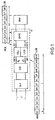
- the translator or transcoder circuit TC forms part of a telephone line circuit LC connected between a telephone line LI and a digital switching network SNW and comprising the cascade connection of a subscriber line interface SLIC able to perform line control and supervision, a digital signal processor DSP mainly adapted to execute analog-to-digital and digital-to-analog conversion operations, the above transcoder circuit TC and a dual processor terminal controller DPTC which deals with the general control of the line circuit.
- the DSP only processes linear PCM signals, whereas the DPTC solely operates on companded PCM signals.
- the purpose of the transcoder circuit TC and more particularly of its COLI circuit is therefore to transcode companded PCM signals received from DPTC on its input terminal IN1 into linear PCM signals which are then transmitted to DSP via output terminal OUT1, and vice-versa in the LICO circuit for the signals received on input terminal IN2 from DSP and transmitted via output terminal OUT2 to DPTC.
- the TC is provided in common for eight DSP and SLIC circuits as indicated by the multiplying arrows but could be used for as much as 32 DPS and SLIC circuit. Indeed, the data received in the TC and transmitted therefrom form part of a 32-channel frame of which only 8 are effectively used and wherein each channel has a repetition period of 125 microseconds.
- the data bits exchanged between TC and DPS have a bit rate of 4,096 Kbit/sec and, each used channel contains a 16-bit PCM signal of which 13 bits b1 to b13 together constitute a linear PCM signal.
- Bit b1 is the sign bit S and bits b2 to b13 define the absolute magnitude J of the signal.
- Bit b1 is preceded by two identical bits and bit b13 is followed by a bit which may be used as a rounding bit.
- This 16-bit pattern is for instance received under a form wherein all bits are inverted and the 2's complement has been taken.
- the data exchanged between TC and DPTC have a bit rate of 2,048 Kbit/sec and each used channel contains an 8-bit companded PCM signal comprising bits b1 to b8.
- This PCM signal is coded according to the segmented logarithmic A-law or mu-law each comprising 8 segments for each of the values of the sign S indicated by bit b1.
- the 3 bits b2 to b4 define one segment K among 8 possible segments K0 to K7 and the bits b5 to b8 define one step L among 16 possible equal steps within the segment.
- the relative values of the step sizes in the segments K0 to K7 are equal to 2° to 2' respectively, whereas in the A law they are 2, 2, 2 2 , ..., 2 7 respectively.
- the companded PCM signal b1 to b8 is for instance received from and transmitted to DPTC under a form wherein all bits except the sign bit are inverted (mu-law) or wherein only the even numbered bits are inverted (A-law).
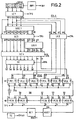
- the COL1 circuit includes an input circuit INP1, a serial-in-parallel-out register SIP01, a parallel-in- serial-out register PISO, a shift register SR, a segment decoder circuit SDEC1, an adder circuit ADD1, an output circuit OC1, a logic circuit LOG1, latch circuits LC1 to LC4, a gating circuit GC and a timing circuit TC which generates timing pulses of which only TP1 to TP7 required to explain the operation of the COL1 circuit are represented in Fig. 5.
- the latch circuits LC1, LC2, LC3 and LC4 are controlled by TP2, TP4, TP3 and TP5 respectively, and gating circuit GC is controlled by TP6.
- the input IN1 of the COL1 circuit is coupled via the input circuit INP1 to that of SIP01 whose outputs are coupled to the inputs of LC1 having output R1 to R4.
- Output R1 is connected to output circuit OC1 via latch circuits LC3 and LC4;
- outputs R2 to R4 are connected to respective inputs of SDEC1 and R1 to R4 are moreover coupled via LC2 to the data inputs 3 of the cells PC2 to PC5 of PISO.
- the latter comprises the interconnected cells PC1 to PC6 with commoned control inputs 4 controlled by timing pulses TP7 as well as commoned control inputs 5 controlled by timing pulses TP3.
- the output 2 of each of these cells is connected to the input 1 of the following one, except for the input 1 of PC1 which is grounded and for the output 2 of PC6 which is connected to the commoned data inputs 3 of the cells PC11 to PC18 of SR.
- the latter cells further have interconnected control inputs 4 controlled by timing pulses TP1, as well as individual control inputs 5.
- the segment decoder circuit SDEC1 has outputs S'0, S'1 and S2 to S7 of which S2 to S7 are coupled via latching circuits LC3 and LC4 and gating circuit GC in cascade to the last mentioned control inputs 5 of the cells PC13 to PC18 of SR.
- the outputs 5'0 and 5'1 of SDEC1 are coupled via latching circuit LC3 to inputs of the logic circuit LOG1 having a further control input A, and outputs a, b and S1, S0.
- the control input A is indicative of A-law or mu-la, A being then 0 and 1 respectively.
- the outputs a and b are connected via LC4 to the data inputs 3 of the cells PC1 and PC6 of PIS01 respectively, whilst the outputs S0 and S1 are coupled via LC4 and GC in cascade to the control inputs 5 of the cells PC11 and PC12 of SR respectively.
- the output 2 of PC11 is coupled to the output circuit OC1 via an adder circuit ADD1 which is also controlled by the above control input A.
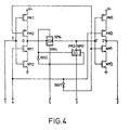
- Each of the cells PC1 to PC6 of PISO is of the type shown in Fig. 4, to be considered with switch S1 only and includes two identical input and output circuits.
- the cell input circuit comprises PMOS transistors PM1 and PM2 and NMOS transistors NM1 and NM2 whose source-to-drain and drain-to-source paths are connected in series between V+ and ground.
- the interconnected gates of PM1 and NM2 and the interconnected drains of PM2 and NM1 constitute the input I and output O of the cell input circuit respectively, the gates of NM1 and of PM1 being controlled from the cell control input 4 directly and via inverter INV1 respectively.
- the constituent components of the output circuit are indicated by the same numeral as in the input circuit, however provided with a prime.
- NM'1 and PM'2 are now controlled from the cell control input 4 via the inverter INV1 and directly respectively.
- the input I and the output O' are connected to the serial data input 1 and to the serial data output 2 of the cell respectively and a parallel data input 3 is coupled to the commoned output O and input I' of the cell input and output circuits through a switch S1.
- the latter comprises PMOS transistor PM3 and NMOS transistor NM3 whose source and drain electrodes are connected to the drain and source electrodes of NM3 and PM3 respectively.
- the gates of NM3 and PM3 are controlled from the control input 5 directly and via an inverter INV2 respectively. It is clear that switch S1 is closed when control input 5 is activated (1).
- Switch S2 is of the same structure as switch S1 but PM4 and NM4 are now controlled from control input 5 directly and via the inverter INV2 respectively, so that switch S2 is closed when control input 5 is deactivated (0).
- a cell circuit PC1/6 of PISO operates as follows. To enter and transfer data applied to the serial input 1, the control input 4 is alternately activated and deactivated and the control input 5 is maintained deactivated, whereas to enter and transfer data applied to the other data input 3 the control inputs 5 and 4 should be simultaneously activated and deactivated respectively.
- the data applied to serial data input 1 are inverted in the cell input circuit and latched in the cell upon control input 4 being activated and then inverted in the cell output circuit and transferred to the cell output 2 upon control input 4 being deactivated.
- data applied to the parallel data input 3 is inverted and transferred to the cell output 2 upon control inputs 5 and 4 being activated and deactivated respectively.
- a cell circuit PC11/18 of SR operates in a similar way as described above for a cell circuit PC1/6, but now the cell input circuit is disconnected from the cell output circuit by switch S2 when time switch S1 is closed and vice-versa since these switches are controlled by opposite control signals.
- the COLI circuit described above is able to calculate this algorithm in the way described hereinafter.
- a companded PCM signal applied to the input IN1 of the COLI1, with the most significant bit (MSB) first, is possibly transformed in input circuit INP1 and the resulting 8-bit companded PCM signal comprising bits b1 to b8 (Fig. 1) and defining S, K and L mentioned above is serially entered into SIP01 as two successive sets of four bits b1 to b4 and b5 to b8.
- this is not correct for segment K0 ⁇ in the A-law since the value of K' has then to be equal to 1 instead of to 0.
- the second set of bits b5b6b7b8 defining the step code L has been entered in SIP01. These bits are latched in LC1 under the control of the second timing pulse TP2 shown and afterwards latched in LC2 by timing pulse TP4. As a consequence these bits b5 to b8 are applied to the data inputs 3 of the respective cells PC2 to PC5 of PISO.
- step code constituted to the bits a, b5, b6, b7, b8, b is now entered in PISO under the control of a second timing pulse TP3 and inverted therein and transferred to the outputs of the cells PC1 to PC6 because timing pulse TP7 is then deactivated.
- a, b5, 66, 67, 68 and b are then present at the outputs of these cells.
- Fig. 3 showing the LICO circuit, of the transcoder TC, which is adapted to transcoder TC, which is adapted to transcode a 13-bit linear PCM word into an 8-bit companded PCM word.
- the LICO circuit is controlled by a timing circuit which is now however not shown as it is obvious from the description of the operation of the LICO circuit which will be given later.
- the LICO circuit includes an input circuit INP2, a 13-cell shift register and latching circuit SRLC, two serial-in-parallel-out registers SIP02 and SIP3, a segment decoder circuit SDEC2, and encoder circuit ENC, an adder circuit ADD2, a logic circuit LOG2, latching circuits LC5 to LC7, output circuit OC2 and switches SW0 to SW7.
- the cells of SIP02 and SIP03 are of the type shown in Fig. 4, however to be considered without S1 and S2. Their control inputs 4 are commoned and controlled by timing pulses TP (not shown).
- the switches SW0 to SW7 are similar to those used in the COLI circuit and as shown in Fig. 4.
- the input IN2 of the LICO circuit is connected via the input circuit INP2 to that of SRLC which includes 13 cells and has an output coupled via adder circuit ADD2 to the input 1 of SIP02.
- An output of the first cell of SRLC is connected to output circuit OC2, and the adder circuit ADD2 is controlled by control input A which is the same as the one and in the COLI circuit and is therefore on 0 for the A-law and on 1 for the mu-law.
- the SIP02 comprises 12 interconnected cells SC1 to SC12 having outputs which are connected to the inputs of the segment decoder SDEC2 which has outputs S'0, S'1, S2,..., coupled via latching circuit LC5 to the encoder ENC.
- the outputs S'0 and S'1 of SDEC2 are also coupled to the inputs of the logic circuit LOG2 which is also provided with control input A and having outputs S0 and S1 which are connected to LC5.
- These outputs S0 ⁇ to S7 of LC5 and also their inverse S0 ⁇ to S7 are connected to the control inputs of the switches SW0 to SW7 respectively.
- the data inputs of these switches are connected to the outputs of the respective cells SC5 to SC12 of PIS02 and their data outputs are commoned and connected to the input of SIP03.
- the outputs of SIP03 and those of the encoder circuit ENC are connected via the respective latch circuits LC6 and LC7 to the output circuit OC2 whose output OUT2 constitutes the output of the LICO.
- K a lower limit is calculated.
- the LICO circuit described above is able to calculate this algorithm in the way described hereinafter.
- the word stored into SIP02 is the altered input word J+c.
- bit b13 is the least significant bit and has the weights 2° the eight bits b2 to b9 define the value (J+c) ⁇ 2 -4 which will now be used to determine This is done by determining only the highest power of 2 of (J+c) ⁇ 2 -4 . This highest power defines the lower limit of the segment, as will be explained later.
- SDEC2 for instance includes a plurality of clocked AND-gates defining the Boolean function b2; b2 ⁇ b3; b2 b3 - b4; ...; b2 b3 b4 b5 b6 b7 b8.
- the output of each of these gates is connected to a corresponding single one of the output leads S7 ... S'0 directly and via inverter to the other ones.
- SDEC2 in fact detects the first 1 in the series of bits b2 to b9, except for K0, and ignores the following binary values in this series. This means that it detects the highest power of 2 and does not take the lower powers of 2 into account.
- each of the segments K0 ⁇ to K7 is defined by its lower limit. K0 ⁇ is detected if all bits b2 to b8 are 0 and independently of bit b9, since one is then sure that segment 0 is concerned.
- the above decimal value of K' can be used for the segments K0 (mu-law) and K2 to K7 (both laws), but not for segment K0 ⁇ (A-law) because in this case the step size is equal to that for segment K1.
- the output signals S'0 ⁇ and S'1 of SDEC2 are supplied to the logic circuit LOG2 which provides at its outputs S0 ⁇ and S1 the signals and The outputs S0 ⁇ to S7, together with S0 ⁇ to S7 , are applied to the control inputs of the switches SW0 to SW7 respectively.
- SIP03 contents of SIP03 are latched in LC6 and thus applied to the output circuit OC2. Therein the sign, the 3-bit segment code and the 4-bit step code are serially applied to the output OUT2.
Landscapes
- Nonlinear Science (AREA)
- Engineering & Computer Science (AREA)
- Theoretical Computer Science (AREA)
- Physics & Mathematics (AREA)
- Compression, Expansion, Code Conversion, And Decoders (AREA)
- Amplifiers (AREA)
- Details Of Television Scanning (AREA)
- Stabilization Of Oscillater, Synchronisation, Frequency Synthesizers (AREA)
- Semiconductor Lasers (AREA)
- Printers Characterized By Their Purpose (AREA)
- Supply And Distribution Of Alternating Current (AREA)
- Emergency Protection Circuit Devices (AREA)
- Transition And Organic Metals Composition Catalysts For Addition Polymerization (AREA)
- Fats And Perfumes (AREA)
- Transmission Systems Not Characterized By The Medium Used For Transmission (AREA)
- Developing Agents For Electrophotography (AREA)
- Diaphragms For Electromechanical Transducers (AREA)
- Mobile Radio Communication Systems (AREA)
- Reduction Or Emphasis Of Bandwidth Of Signals (AREA)
- Glass Compositions (AREA)
- Synchronisation In Digital Transmission Systems (AREA)
- Silicon Polymers (AREA)
- Organic Low-Molecular-Weight Compounds And Preparation Thereof (AREA)
- Cereal-Derived Products (AREA)
- Measurement Of Velocity Or Position Using Acoustic Or Ultrasonic Waves (AREA)
- Arrangements For Transmission Of Measured Signals (AREA)
- Investigating Or Analyzing Materials By The Use Of Ultrasonic Waves (AREA)
- Steroid Compounds (AREA)
- Optical Fibers, Optical Fiber Cores, And Optical Fiber Bundles (AREA)
- Signal Processing For Digital Recording And Reproducing (AREA)
- Dc Digital Transmission (AREA)
- Control Of Motors That Do Not Use Commutators (AREA)
- Interface Circuits In Exchanges (AREA)
Priority Applications (1)
| Application Number | Priority Date | Filing Date | Title |
|---|---|---|---|
| AT84201345T ATE51986T1 (de) | 1983-09-19 | 1984-09-15 | Pcm-signalumsetzer. |
Applications Claiming Priority (2)
| Application Number | Priority Date | Filing Date | Title |
|---|---|---|---|
| BE2060209 | 1983-09-19 | ||
| BE2/60209A BE897773A (nl) | 1983-09-19 | 1983-09-19 | Pulse code modulatie omzetter |
Publications (3)
| Publication Number | Publication Date |
|---|---|
| EP0145039A2 EP0145039A2 (en) | 1985-06-19 |
| EP0145039A3 EP0145039A3 (en) | 1986-12-30 |
| EP0145039B1 true EP0145039B1 (en) | 1990-04-11 |
Family
ID=3865654
Family Applications (1)
| Application Number | Title | Priority Date | Filing Date |
|---|---|---|---|
| EP84201345A Expired - Lifetime EP0145039B1 (en) | 1983-09-19 | 1984-09-15 | Pulse code modulation translators |
Country Status (23)
| Country | Link |
|---|---|
| US (1) | US4610018A (tr) |
| EP (1) | EP0145039B1 (tr) |
| JP (1) | JPS60178716A (tr) |
| KR (1) | KR850002716A (tr) |
| AT (1) | ATE51986T1 (tr) |
| AU (3) | AU570501B2 (tr) |
| BE (1) | BE897773A (tr) |
| BR (1) | BR8404596A (tr) |
| CA (1) | CA1249371A (tr) |
| DD (1) | DD229258A5 (tr) |
| DE (1) | DE3481964D1 (tr) |
| EG (1) | EG16761A (tr) |
| ES (1) | ES8701438A1 (tr) |
| FI (1) | FI843642A7 (tr) |
| HU (1) | HU198257B (tr) |
| MX (1) | MX161788A (tr) |
| NO (1) | NO843683L (tr) |
| PT (1) | PT79225B (tr) |
| RO (1) | RO91607B (tr) |
| SU (1) | SU1702879A3 (tr) |
| TR (1) | TR22618A (tr) |
| YU (1) | YU45660B (tr) |
| ZA (1) | ZA847074B (tr) |
Cited By (1)
| Publication number | Priority date | Publication date | Assignee | Title |
|---|---|---|---|---|
| US11553999B2 (en) | 2017-03-31 | 2023-01-17 | Trisa Holding Ag | Electrical body care brush |
Families Citing this family (10)
| Publication number | Priority date | Publication date | Assignee | Title |
|---|---|---|---|---|
| GB2178879A (en) * | 1985-08-09 | 1987-02-18 | Plessey Co Plc | Signal conversion circuits |
| CA1240063A (en) * | 1986-02-25 | 1988-08-02 | Milan Skubnik | Digital companding circuit |
| NO180137C (no) * | 1986-11-17 | 1997-02-19 | Alcatel Nv | Ekkokansellerings-anlegg |
| FR2612024A1 (fr) * | 1987-02-25 | 1988-09-09 | Mitel Corp | Circuit de compression et d'extension de signaux numeriques |
| EP0455893B1 (en) * | 1990-05-11 | 1995-02-01 | Alcatel N.V. | Telecommunication line circuit |
| US5646946A (en) * | 1995-10-30 | 1997-07-08 | Motorola, Inc. | Apparatus and method for selectively companding data on a slot-by-slot basis |
| US5883925A (en) * | 1995-11-16 | 1999-03-16 | International Business Machines Corporation | Pulse code modulation compression mechanism |
| US5991278A (en) | 1996-08-13 | 1999-11-23 | Telogy Networks, Inc. | Asymmetric modem communications system and method |
| US6549569B1 (en) | 1999-04-09 | 2003-04-15 | Siemens Information & Communication Networks, Inc. | System and method for improving conversion between A-law and U-law coding |
| KR101418711B1 (ko) * | 2012-12-27 | 2014-08-06 | 주식회사 선익시스템 | 기판 얼라인 모듈과 이를 구비한 증착장치 |
Family Cites Families (9)
| Publication number | Priority date | Publication date | Assignee | Title |
|---|---|---|---|---|
| DE2011056B2 (de) * | 1970-03-09 | 1971-12-16 | Krone Gmbh, 1000 Berlin | Pulscodedemodulator mit dehnercharakteristik aufweisender knickkennlinie |
| US3778605A (en) * | 1971-04-16 | 1973-12-11 | Bell Telephone Labor Inc | Digital expandor for pcm code words |
| US3937897A (en) * | 1974-07-25 | 1976-02-10 | North Electric Company | Signal coding for telephone communication system |
| GB1597468A (en) * | 1977-06-02 | 1981-09-09 | Post Office | Conversion between linear pcm representation and compressed pcm |
| JPS55117332A (en) * | 1979-03-02 | 1980-09-09 | Fujitsu Ltd | Code converting system |
| US4311988A (en) * | 1979-04-05 | 1982-01-19 | Motorola Inc. | Programmable A-law and μ-law DAC |
| JPS5627546A (en) * | 1979-08-13 | 1981-03-17 | Nec Corp | Block compressing coder |
| DE3104513C2 (de) * | 1981-02-09 | 1983-03-31 | Siemens AG, 1000 Berlin und 8000 München | Verfahren zur Umwandlung linear codierter PCM-Worte in nichtlinear codierte PCM-Worte und umgekehrt nichtlinear codierter PCM-Worte in linear codierte PCM-Worte gemäß einer dem A-Gesetz gehorchenden 13-Segment-Kennlinie |
| US4370632A (en) * | 1981-05-08 | 1983-01-25 | Motorola, Inc. | Multiple function operational amplifier circuit |
-
1983
- 1983-09-19 BE BE2/60209A patent/BE897773A/nl not_active IP Right Cessation
-
1984
- 1984-09-07 ZA ZA847074A patent/ZA847074B/xx unknown
- 1984-09-13 AU AU32999/84A patent/AU570501B2/en not_active Ceased
- 1984-09-13 US US06/650,336 patent/US4610018A/en not_active Expired - Lifetime
- 1984-09-14 BR BR8404596A patent/BR8404596A/pt not_active IP Right Cessation
- 1984-09-15 AT AT84201345T patent/ATE51986T1/de not_active IP Right Cessation
- 1984-09-15 EP EP84201345A patent/EP0145039B1/en not_active Expired - Lifetime
- 1984-09-15 DE DE8484201345T patent/DE3481964D1/de not_active Expired - Lifetime
- 1984-09-17 SU SU843793654A patent/SU1702879A3/ru active
- 1984-09-17 NO NO843683A patent/NO843683L/no unknown
- 1984-09-18 CA CA000462951A patent/CA1249371A/en not_active Expired
- 1984-09-18 DD DD84267376A patent/DD229258A5/de unknown
- 1984-09-18 FI FI843642A patent/FI843642A7/fi not_active Application Discontinuation
- 1984-09-18 RO RO115734A patent/RO91607B/ro unknown
- 1984-09-18 TR TR6159/84A patent/TR22618A/tr unknown
- 1984-09-18 YU YU160484A patent/YU45660B/sh unknown
- 1984-09-19 KR KR1019840005738A patent/KR850002716A/ko not_active Ceased
- 1984-09-19 PT PT79225A patent/PT79225B/pt unknown
- 1984-09-19 HU HU843525A patent/HU198257B/hu not_active IP Right Cessation
- 1984-09-19 JP JP59196520A patent/JPS60178716A/ja active Pending
- 1984-09-19 EG EG581/84A patent/EG16761A/xx active
- 1984-09-19 ES ES84536073A patent/ES8701438A1/es not_active Expired
- 1984-09-19 MX MX202765A patent/MX161788A/es unknown
-
1987
- 1987-12-16 AU AU82634/87A patent/AU592028B2/en not_active Ceased
- 1987-12-16 AU AU82633/87A patent/AU590138B2/en not_active Ceased
Cited By (2)
| Publication number | Priority date | Publication date | Assignee | Title |
|---|---|---|---|---|
| US11553999B2 (en) | 2017-03-31 | 2023-01-17 | Trisa Holding Ag | Electrical body care brush |
| US12575919B2 (en) | 2017-03-31 | 2026-03-17 | Trisa Holding Ag | Electrical body care brush |
Also Published As
| Publication number | Publication date |
|---|---|
| DE3481964D1 (de) | 1990-05-17 |
| BE897773A (nl) | 1984-03-19 |
| ATE51986T1 (de) | 1990-04-15 |
| CA1249371A (en) | 1989-01-24 |
| ZA847074B (en) | 1985-04-24 |
| EP0145039A2 (en) | 1985-06-19 |
| SU1702879A3 (ru) | 1991-12-30 |
| RO91607A (ro) | 1987-05-15 |
| PT79225A (en) | 1984-10-01 |
| YU45660B (sh) | 1992-07-20 |
| JPS60178716A (ja) | 1985-09-12 |
| HUT38770A (en) | 1986-06-30 |
| EG16761A (en) | 1989-06-30 |
| BR8404596A (pt) | 1985-08-06 |
| TR22618A (tr) | 1988-01-11 |
| NO843683L (no) | 1985-03-20 |
| AU570501B2 (en) | 1988-03-17 |
| AU8263387A (en) | 1988-04-14 |
| EP0145039A3 (en) | 1986-12-30 |
| AU590138B2 (en) | 1989-10-26 |
| FI843642L (fi) | 1985-03-20 |
| RO91607B (ro) | 1987-05-31 |
| KR850002716A (ko) | 1985-05-15 |
| ES536073A0 (es) | 1986-10-16 |
| FI843642A0 (fi) | 1984-09-18 |
| DD229258A5 (de) | 1985-10-30 |
| PT79225B (en) | 1986-08-22 |
| AU592028B2 (en) | 1989-12-21 |
| YU160484A (en) | 1987-10-31 |
| FI843642A7 (fi) | 1985-03-20 |
| AU8263487A (en) | 1988-04-14 |
| US4610018A (en) | 1986-09-02 |
| AU3299984A (en) | 1985-03-28 |
| ES8701438A1 (es) | 1986-10-16 |
| MX161788A (es) | 1990-12-27 |
| HU198257B (en) | 1989-08-28 |
Similar Documents
| Publication | Publication Date | Title |
|---|---|---|
| EP0145039B1 (en) | Pulse code modulation translators | |
| US4387457A (en) | Digital conference circuit and method | |
| KR20010062661A (ko) | 패스트 하다마드 변환 디바이스 | |
| US4837617A (en) | Method and means for coding and decoding picture information | |
| EP0429092B1 (en) | Integrated digital circuit for processing speech signal | |
| IE49738B1 (en) | Telephone summing circuit | |
| JPS6118910B2 (tr) | ||
| US4393367A (en) | Digital compandor having nonlinear companding characteristics | |
| GB1597468A (en) | Conversion between linear pcm representation and compressed pcm | |
| JPS6347372B2 (tr) | ||
| GB2316511A (en) | Accumulator circuit and method of use thereof | |
| US6055275A (en) | ADPCM transcoder | |
| EP0167677A1 (en) | Signal processing arrangement | |
| EP0067006B1 (en) | Digital conference circuit and method | |
| US3612772A (en) | Circuit for adding codes resulting from nonlinear coding | |
| KR920004348B1 (ko) | Pcm 부호 복호기 | |
| PL152068B1 (pl) | Translator sygnałów modulowanych kodowo-impulsowo | |
| EP0215167A1 (en) | Instant speaker algorithm for digital conference bridge | |
| JPS61247195A (ja) | レベル可変回路 | |
| AU643826B2 (en) | Bit finder circuit | |
| JPS61169029A (ja) | 双方向時分割多重化dpcm符号復号器 | |
| JPH0575472A (ja) | 復号化回路 | |
| JPH07264285A (ja) | ネットワークシステム | |
| KR960039625A (ko) | 아날로그 신호 전송을 위한 스위치 | |
| JPH1039755A (ja) | ディジタル・データ・シャッフル/デ・シャッフル方式 |
Legal Events
| Date | Code | Title | Description |
|---|---|---|---|
| PUAI | Public reference made under article 153(3) epc to a published international application that has entered the european phase |
Free format text: ORIGINAL CODE: 0009012 |
|
| AK | Designated contracting states |
Designated state(s): AT BE CH DE FR GB IT LI NL SE |
|
| PUAL | Search report despatched |
Free format text: ORIGINAL CODE: 0009013 |
|
| AK | Designated contracting states |
Kind code of ref document: A3 Designated state(s): AT BE CH DE FR GB IT LI NL SE |
|
| 17P | Request for examination filed |
Effective date: 19870708 |
|
| RAP1 | Party data changed (applicant data changed or rights of an application transferred) |
Owner name: ALCATEL N.V. Owner name: BELL TELEPHONE MANUFACTURING COMPANY NAAMLOZE VENN |
|
| RAP3 | Party data changed (applicant data changed or rights of an application transferred) |
Owner name: ALCATEL N.V. Owner name: BELL TELEPHONE MANUFACTURING COMPANY NAAMLOZE VENN |
|
| 17Q | First examination report despatched |
Effective date: 19880629 |
|
| ITF | It: translation for a ep patent filed | ||
| GRAA | (expected) grant |
Free format text: ORIGINAL CODE: 0009210 |
|
| AK | Designated contracting states |
Kind code of ref document: B1 Designated state(s): AT BE CH DE FR GB IT LI NL SE |
|
| REF | Corresponds to: |
Ref document number: 51986 Country of ref document: AT Date of ref document: 19900415 Kind code of ref document: T |
|
| REF | Corresponds to: |
Ref document number: 3481964 Country of ref document: DE Date of ref document: 19900517 |
|
| ET | Fr: translation filed | ||
| PLBE | No opposition filed within time limit |
Free format text: ORIGINAL CODE: 0009261 |
|
| STAA | Information on the status of an ep patent application or granted ep patent |
Free format text: STATUS: NO OPPOSITION FILED WITHIN TIME LIMIT |
|
| 26N | No opposition filed | ||
| PG25 | Lapsed in a contracting state [announced via postgrant information from national office to epo] |
Ref country code: DE Effective date: 19910601 |
|
| ITTA | It: last paid annual fee | ||
| PGFP | Annual fee paid to national office [announced via postgrant information from national office to epo] |
Ref country code: CH Payment date: 19911213 Year of fee payment: 8 |
|
| NLS | Nl: assignments of ep-patents |
Owner name: ALCATEL N.V. TE AMSTERDAM. |
|
| PGFP | Annual fee paid to national office [announced via postgrant information from national office to epo] |
Ref country code: GB Payment date: 19920820 Year of fee payment: 9 |
|
| PG25 | Lapsed in a contracting state [announced via postgrant information from national office to epo] |
Ref country code: LI Effective date: 19920930 Ref country code: CH Effective date: 19920930 |
|
| REG | Reference to a national code |
Ref country code: CH Ref legal event code: PL |
|
| PG25 | Lapsed in a contracting state [announced via postgrant information from national office to epo] |
Ref country code: GB Effective date: 19930915 |
|
| GBPC | Gb: european patent ceased through non-payment of renewal fee |
Effective date: 19930915 |
|
| EAL | Se: european patent in force in sweden |
Ref document number: 84201345.0 |
|
| PGFP | Annual fee paid to national office [announced via postgrant information from national office to epo] |
Ref country code: AT Payment date: 19950911 Year of fee payment: 12 |
|
| PG25 | Lapsed in a contracting state [announced via postgrant information from national office to epo] |
Ref country code: AT Effective date: 19960915 |
|
| PGFP | Annual fee paid to national office [announced via postgrant information from national office to epo] |
Ref country code: NL Payment date: 19960919 Year of fee payment: 13 |
|
| PG25 | Lapsed in a contracting state [announced via postgrant information from national office to epo] |
Ref country code: NL Free format text: LAPSE BECAUSE OF NON-PAYMENT OF DUE FEES Effective date: 19980401 |
|
| NLV4 | Nl: lapsed or anulled due to non-payment of the annual fee |
Effective date: 19980401 |
|
| PGFP | Annual fee paid to national office [announced via postgrant information from national office to epo] |
Ref country code: FR Payment date: 19980821 Year of fee payment: 15 |
|
| PGFP | Annual fee paid to national office [announced via postgrant information from national office to epo] |
Ref country code: SE Payment date: 19980824 Year of fee payment: 15 |
|
| PGFP | Annual fee paid to national office [announced via postgrant information from national office to epo] |
Ref country code: BE Payment date: 19980908 Year of fee payment: 15 |
|
| PG25 | Lapsed in a contracting state [announced via postgrant information from national office to epo] |
Ref country code: SE Free format text: THE PATENT HAS BEEN ANNULLED BY A DECISION OF A NATIONAL AUTHORITY Effective date: 19990929 |
|
| PG25 | Lapsed in a contracting state [announced via postgrant information from national office to epo] |
Ref country code: BE Free format text: LAPSE BECAUSE OF NON-PAYMENT OF DUE FEES Effective date: 19990930 |
|
| BERE | Be: lapsed |
Owner name: ALCATEL BELL Effective date: 19990930 |
|
| EUG | Se: european patent has lapsed |
Ref document number: 84201345.0 |
|
| PG25 | Lapsed in a contracting state [announced via postgrant information from national office to epo] |
Ref country code: FR Free format text: LAPSE BECAUSE OF NON-PAYMENT OF DUE FEES Effective date: 20000531 |
|
| REG | Reference to a national code |
Ref country code: FR Ref legal event code: ST |