EP0133586A1 - Vorrichtung und Verfahren zur Erzeugung eines Stehbildvideosignals mittels einer Festkörper-Bildanordnung - Google Patents
Vorrichtung und Verfahren zur Erzeugung eines Stehbildvideosignals mittels einer Festkörper-Bildanordnung Download PDFInfo
- Publication number
- EP0133586A1 EP0133586A1 EP84109564A EP84109564A EP0133586A1 EP 0133586 A1 EP0133586 A1 EP 0133586A1 EP 84109564 A EP84109564 A EP 84109564A EP 84109564 A EP84109564 A EP 84109564A EP 0133586 A1 EP0133586 A1 EP 0133586A1
- Authority
- EP
- European Patent Office
- Prior art keywords
- image signal
- signal
- solid
- memory
- imaging device
- Prior art date
- Legal status (The legal status is an assumption and is not a legal conclusion. Google has not performed a legal analysis and makes no representation as to the accuracy of the status listed.)
- Granted
Links
- 238000003384 imaging method Methods 0.000 title claims abstract description 65
- 238000004519 manufacturing process Methods 0.000 title description 2
- 238000006243 chemical reaction Methods 0.000 claims abstract description 58
- 238000013139 quantization Methods 0.000 claims abstract description 21
- 238000000034 method Methods 0.000 claims description 4
- 230000003287 optical effect Effects 0.000 description 8
- 230000004044 response Effects 0.000 description 8
- 230000000694 effects Effects 0.000 description 5
- 238000010586 diagram Methods 0.000 description 4
- 238000005070 sampling Methods 0.000 description 3
- 239000004065 semiconductor Substances 0.000 description 2
- 238000013459 approach Methods 0.000 description 1
- 238000004040 coloring Methods 0.000 description 1
- 238000012937 correction Methods 0.000 description 1
- 230000007423 decrease Effects 0.000 description 1
- 230000006866 deterioration Effects 0.000 description 1
- 238000012986 modification Methods 0.000 description 1
- 230000004048 modification Effects 0.000 description 1
- 238000012545 processing Methods 0.000 description 1
- 239000007787 solid Substances 0.000 description 1
- 238000012546 transfer Methods 0.000 description 1
Images


Classifications
-
- H—ELECTRICITY
- H04—ELECTRIC COMMUNICATION TECHNIQUE
- H04N—PICTORIAL COMMUNICATION, e.g. TELEVISION
- H04N25/00—Circuitry of solid-state image sensors [SSIS]; Control thereof
- H04N25/60—Noise processing, e.g. detecting, correcting, reducing or removing noise
- H04N25/616—Noise processing, e.g. detecting, correcting, reducing or removing noise involving a correlated sampling function, e.g. correlated double sampling [CDS] or triple sampling
-
- H—ELECTRICITY
- H04—ELECTRIC COMMUNICATION TECHNIQUE
- H04N—PICTORIAL COMMUNICATION, e.g. TELEVISION
- H04N25/00—Circuitry of solid-state image sensors [SSIS]; Control thereof
- H04N25/50—Control of the SSIS exposure
- H04N25/53—Control of the integration time
-
- H—ELECTRICITY
- H04—ELECTRIC COMMUNICATION TECHNIQUE
- H04N—PICTORIAL COMMUNICATION, e.g. TELEVISION
- H04N25/00—Circuitry of solid-state image sensors [SSIS]; Control thereof
- H04N25/60—Noise processing, e.g. detecting, correcting, reducing or removing noise
- H04N25/618—Noise processing, e.g. detecting, correcting, reducing or removing noise for random or high-frequency noise
Definitions
- This invention relates generally to still image pickup apparatus, and particularly to such an apparatus and method for producing a still image video signal using a solid-state imaging device.
- Still image pickup apparatus is arranged to store a video signal or a picture signal from an image-pickup device so that the picture signal corresponding to a field or frame is repeatedly read out from a memory.
- a solid-state imaging device such as a CCD imaging device
- such still image pickup apparatus has hitherto been unsatisfactory because high-quality image cannot be obtained for the following reasons.
- a reproduced still picture is apt to suffer from a fixed pattern of specks due to variations in magnitude of photoelectric conversion signal resulted from scattering of reading out efficiency throughout respective pixels (picture elements) of the solid-state imaging device. Furthermore, in addition to the above reason because of variations in magnitude of photoelectric conversion signal resulted from nonlinear error caused from the scattering of transfer efficiency throughout respective pixels, nonlinear distorition occurs in dark portions in the reproduced picture. Moreover, the dark portion in the rproduced picture shows low luminance, while coloring of the dark portion occurs due to color false signals.
- the present invention has been developed in order to remove the above-described drawbacks inherent to the conventional still image pickup apparatus using one or more solid-state imaging device.
- an object of the present invention to provide a new and useful still image pickup apparatus using one or more solid-state imaging device so that a satisfactory reproduced still picture of high quality is obtained.
- a solid-state imaging device responsive to incident light carrying optical information of an object to be taken, is used such that an image signal including photoelectric conversion signals from the solid-state imaging device is read out twice or or more, and video image signals read out in twice or more are processed by using a memory so that a resultant sum image signal is produced with the image siqnals beinq added to each other.
- a still image pickup apparatus comprising: first means for passing a light ray from an object for a predetermined period of time; a solid-state image pickup device responsive to said light ray from said first means for producing photoelectric conversion signals in respective pixels thereof; second means for reading out said photoelectric conversion signals as an image signal from said solid-state image pickup device in twice or more; third means for storing a first image signal resulted from a first time reading out; and fourth means for adding said first image signal read out from said third means to a second image signal from said solid-state imaging device so that two image signals respectively resulted from first and second readings are added to each other for producing a resultant sum image signal.
- a still image pickup apparatus comprising: first means for passing a light ray from an object for a predetermined period of time; a solid-state image pickup device responsive to said light ray from said first means for producing photoelectric conversion signals in respective pixels thereof; second means for reading out said photoelectric conversion signals as an image signal from said solid-state image pickup device in twice or more; an A/D converter responsive to said image signal from said solid-state image pickup device; a memory responsive to a digital signal from said A/D converter for storing a first image signal resulted from a first time reading out; a digital adder responsive to said first image signal read out from said memory and to a second image signal resulted from a second time reading out for producing a resultant sum image signal by adding said image first and second signals to each other; a memory control circuit for controlling reading and writing operations of said memory, said resultant sum image signal being written into said memory via said memory control circuit and is read out cyclically; and a D/A converter responsive to said resultant
- a method of producing a still image video signal using at least one solid-state imaging device comprising the steps of: applying a light ray from an object to said solid-state imaging device for a predetermined period of time; performing a first time reading so that a first image signal including photoelectric conversion signals generated in said solid-state imaging device is read out; converting the read out first image signal into a first digital signal; storing said first digital signal into a memory; performing a second time reading so that a second image signal including photoelectric conversion signals generated in said solid-state imaging device is read out; converting said second image signal into a second digital signal; reading out said first digital signal from said memory; adding said second digital signal to said first digital signal for obtaining a resultant sum image signal; storing said resultant sum image signal into said memory so that said first digital signal is renewed by said resultant sum image signal; reading out said resultant sum image signal from said memory cyclically; and converting said resultant sum image signal into an analog image signal.
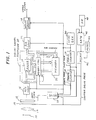
- FIG. 1 a schematic block diagram of an embodiment of the still image pickup apparatus according to the present invention is shown.
- the embodiment comprises an optical system 12 for collecting and focussing a light ray from an object 10 to be taken.
- the optical system 12 is represented by a symbol of a convex lens.
- the light ray passed through the optical system 12 is applied via a shutter 14 to a solid-state imaging device 16, such as a CCD imaging device.
- the shutter 14 is responsive to a drive signal from a mostable multivibrator 42 so as to open for a predetermined period of time to apply the light ray from the optical system 12 to the solid-state imaging device 16 for the predetermined period of time.
- the monostable multivibrator 42 is responsive to a trigger pulse fed from a manually operable switch 40 so as to produce a pulse signal having the predetermined period of time.
- the width of the pulse from the monostable multivibrator 42 may be controlled by way of an adjusting circuit 44 which changes time constant of the monostable multivibrator 42 thereby selecting a desired shutter speed.
- the solid-state imaging device 16 is reponsive to shift clock pulses from a drive circuit 28 which selectively passes sync pulses from a sync pulse generator 30.
- the embodiment of Fig. 1 also comprises an analog-to-digitla (A/D) converter 18, a digital signal prosessor 20, a digital-to-analog (D/A) converter 22, an analog signal processor 24, a semiconductor memory 26, and first and second counters 32 and 38.
- the first counter 32 is responsive to the pulses from the sync pulse generator 30, while the second counter 38 is responsive to pulses from the first counter 32. More specifically, the first counter 32 produces vertical sync pulses each time the number of pulses from the sync pulse generator 30 reaches a predetermined number equal to the number of pixels of the solid-state imaging device 16. With this arrangement, the vertical sync pulse, therefore, represents each field.
- the first counter 32 is referred to as a field counter, and the vertical sync pulse is referred to as a field pulse.
- the field pulse is fed to a gate circuit 46 responsive to a trigger signal from the switch 40 so that the shutter 14 opens in response to a field pulse after the switch 40 is manipulated.
- the second counter 38 counts the number of the vertical sync pulses from the first counter 32 to produce an output pulse when the number of the vertical sync pulses reaches a predetermined value which is two or more. This number is determined depending on the number of times of reading out from the solid-state imaging device 16 as will be described in detail hereinlater.
- the second counter 38 which counts the number of field pulses from the field counter 32 is referred to as a frame counter.
- the digital signal processor 20 comprises a digital adder 34 and a memory control circuit 36 which controls the memory 26 used for storing a digital video signal from the A/D converter 18 and also another digital video signal from the adder 34 arranged to add a digital video signal from the A/D converter 18 to another digital video signal read out from the memory 26.
- the analog signal processor 24 per se is of a conventional circuit which processes an analog video signal for producing output video signal of a desired format, such as NTSC.
- Fig. 1 operates as follows. Assuming that the shutter 14 is driven to open the same for a predeterming period of time, the light ray from the object 10 is incident on the surface of the solid-state imaging device 16 for the predetermined period of time. As a result, the solid-state imaging device 16 produces a charge or photoelectric conversion signal at each pixel thereof. When the output pulse from the monostable multivibrator 42 turns low to close the shutter 14, the drive circuit 28 is enabled to pass the sync pulses from the sync pulse generator 30 in response to the field and/or frame pulse.
- shift clock pulses are fed to the solid-state imaging device 16 to shift charges or photoelectric conversion signals within the solid-state imaging device 16 so that the photoelectric conversion signal is outputted from an output terminal of the solid-state imaging device 16 and is applied to an input terminal of the A/D converter 18 which cyclically converts the analog photoelectric conversion singal into a digital signal at a predetermined sampling interval defined by a sampling pulse signal.
- this sampling pulse signal is used the output pulse signal from the sync pulse generator 30 so that the photoelectric conversion siganl is converted into a digital signal or word such that one digital data is obtained for each pixel of the solid-state imaging device 16.
- the digital word obtained at an output port of the A/D converter 18 is fed to the digital signal processor 20.
- the digital words indicative of video information from respective pixels are fed via the memory control circuit 36 to the memory 26 to be stored therein.
- the memory control circuit 36 is responsive to the pulses from the sync pulse generator 30 and to an output pulse from the frame counter 38.
- video information of all the pixels of the solid-state imaging device 16 is stored in sequence in the memory 26 at different addresses which are disignated by address-disignating signal fed from the memory control circuit 36 via an address bus.
- the memory control circuit 36 also produces a read/write control signal which is fed to the memory 26 for effecting read/write control of the memory 26, in response to the frame pulse.
- the photoelectric conversion signals generated in the pixels of the solid-state imaging device 16 resulted from the application of an optical image of the object 10 for a predetermined period of time, are repeatedly read out for a plurality of times after the shutter 14 is closed.
- a set of photoelectric conversion signals obtained from all the pixels is referred to as an image signal, and is processed such that a resultant sum image signal is obtained by the digital signal processor 20 by adding a latest image signal to a former image signal or a previously produced sum image signal stored in the memory 26.
- the resultant sum image signal is obtained by adding two or more image signals of an identical object 10 such that image singals for the same pixel are added to each other, the above-mentioned problems inherent to the conventionl apparatus are effectively removed. This point will be further described. Since the solid-state imaging device 16 is exposed to incident light for a predetermined period of time in a still image pickup apparatus, the magnitude of the photoelectric conversion signal or charge generated and stored in each pixel in correspondence with optical information of the object 10 decreases each time the photoelectric conversion signal is read out.
- Fig. 2 shows the ralationship between the magnitude of the photoelectric conversion signal generated within the solid-state imaging device 16 and the magnitude of residual signal which remains in the solid-state imaging device 16 after signal read out.
- a curve “A” indicates such a relationship under a condition where the photoelectric conversion signal is not yet read out.
- a curve “B” indicates such a relationship under a condition where the photoelectric conversion signal has been read out once
- another curve “C” indicatess such a relationship under a condition where the photoelectric conversion signal has been read out in twice.
- the reading out efficiency of photoelectric conversion signal varies in accordance with the magnitude of the iniatially generated photoelectric conversion signal within the solid-state imaging device 16. Furthermore, the reading out efficiency of photoelectric conversion signal varies throughout pixels due to variations in semiconductor characteristics. Therefore, when the photoelectric conversion signal is read out from each pixel only once as in the conventional apparatus, the derived photoelectric conversion signal causes various problems described at the beginning of the specification.
- reading out from the solid-state imaging device 16 is effected twice or more so that a plurality of photoelectric conversion signals read out from the same pixel are added to each other to obtain a resultant sum image signal.
- the resultant sum image signal carries information accurately corresponding to optical information of the object 10.
- a trigger pulse is generated in response to a subsequent field pulse to cause the monostable multivibrator 42 to produce a shutter drive pulse having a predetermined width which is adjustable by the adjusting circuit 44.
- the shutter 14 is arranged to open in response to a leading edge of the shutter drive pulse and to close in response to a trailing edge thereof. As the shutter 14 opens, the light ray from the object 10 is incident on the solid-state imaging device 16 to generate charges at respect pixels thereof in accordance with an image of the object 10.
- the frame counter 38 starts counting the number of field pulses. Let us assume that the frame counter 38 is arranged to output a frame pulse when two field pulses are counted. In respose to a second field pulse detected after count-starting, the frame counter 38 produces a frame pulse which causes the drive circuit 28 to start sending shift clock pulses to the solid-state imaging device 16.
- the solid-state imaging device 16 is driven by the shift clock pulses so that photoelectric conversion signals respectively corresponding to pixels thereof are outputted in sequence.
- a set of photoelectric conversion signals corresponding to all the pixels forming an odd field and an even field is referred to as an image signal.
- This image signal resulted from first time reading out is A/D converted by the A/D converter 18 such that each photoelectric conversion signal of each pixel is converted into a digital word.
- the drive circuit 28 Since the reading out is effected with interlace for obtaining odd and even field output signals for each frame, the drive circuit 28 is responsive to the field pulses and frame pulses from the field counter 32 and the frame counter 38.
- the solid-state imaging device 16 is further driven so as to effect a second time reading out for producing a second image signal when the shutter 14 is still kept closed.
- This second image signal is converted into a number of digital words in the same manner as the first-mentioned image signal.
- the digital words corresponding to the second image signal are not stored in the memory 26 but are fed to the adder 34 to be added to the first-mentioned digital words which are read out from the memory 26. This addition is performed such that each digital word resulted from the second time reading out is added to each digital word resulted from the first time reading out so that two photoelectric conversion signals respectiely derived from an identical pixel are added to each other.
- a resultant sum image signal in the form of a number of digital words is obtained at the output port of the adder 34.
- This resultant sum image signal is stored in the memory 26 via the memory control circuit 36 by rewriting the first set of digital words.
- the first set of digital words representing the photoelectric conversion signals resulted from the first time reading out are renewed or updatad with the set of digital words corresponding to the resultant sum image signal.
- the memory control circuit 36 produces a WRITE signal in response to a first frame pulse so that the memory 26 is put in WRITE mode until a second frame pulse is applied. Therefore, the image signal resulted from the first time reading out is stored into the memory 26.
- the memory control circuit 36 produces a WRITE & READ signal so that the memory 26 is put in WRITE & READ mode until a third frame pulse is applied thereby each digital word stored in the memory 26 is read out to be added to a digital word of the second image signal for producing a resultant sum image digital word which is stored in the memory 26 in turn.
- both the solid-state imaging device 16 and the memory control circuit 36 are controlled by the frame pulse from the frame counter 38 so as to establish synchronization for adding the second image signal from the A/D converter 18 to the first image signal read out from the memory 26 such that two digital words representing photoelectric conversion signals from an indentical pixel are added to each other. In this way all the digital words stored in the memory 26 are renewed or updated.
- the memory control circuit 36 produce a READ signal which causes the memory 26 to assume a READ mode. Therefore, the digital words stored in the memory 26 are reapeatedly read out to be fed to the D/A converter 22.
- the digital signal processor 20 operates as follows. Reading out from the solid-state iamging device 16 of the first and second times is effected in the same manner as described in the above.
- the solid-state imaging device 16 When the solid-state imaging device 16 is driven to effect a third time reading out for obtaining a third set of digital words at the output port of the A/D converter 18, then the third set of digital words are added to the digital words corresponding to the reultant sum image signal which is previously stored and read out from the memory 26. In this way, as the solid-state imaging device 16 is driven to effect reading out a plurality of times, the cotents of the memory 26 are renewed in sequence. Accordingly, when a last time reading out is performed, a resultant sum image signal obtained at the output terminal of the adder 34 represents the sum of photoelectric conversion signals resulted from the last time reading out and photoelectric conversion signals updated within the memory 26.
- the finally obtained resultant sum signal at the end of the last reading out represents the total sum of photoelectric conversion signals obtained through a plurality of readings.
- This finally obtained resultant sum signal is also stored in the memory 26, and is then read out repeatedly in the same manner as described in the above.
- the number of times of reading out may be any number which is more than one. Although the number of times of reading out is desired to be a large number so as to obtain more accurate output information, the number of times of reading out may be set to two by omitting third and the following reading out if necessary correction is performed. More specifically, since the tendency of the variation in the magnitude of residual photoelectric conversion signals ramain in the solid-state imaging device 16 after the second time reading out is substantially the same irrespective of the number of times of reading out, third and more time reading out can be omitted with the photoelectric conversion signal resulted from the second time reading out being multiplied by a coefficient of 1 to 1.5 before addition.
- Fig. 4 showing another embodiment in which reading out from the solid-state imaging device 16 is effected only twice.
- the embodiment of Fig. 4 differs from the embodiment of Fig. 1 in that a multiplier 50 is interposed between the output port of the A/D converter 18 and an input port of the adder 34.
- the multiplier 50 is arranged to multiply each digital word by a predetermined coefficient, such as 1 to 1.5.
- the output port of the A/D converter 18 is directly connected to the memory control 36 in the same manner as in the first-described embodiment so that the first set of digital words resulted from first time reading out are stored in the memory 26 without multiplication. Therefore, multiplication is performed in connection with the second set of digital words resulted from the second time reading out.
- the level of quantization noise generated in the A/D converter 18 is constant.
- a non-linear quantization characteristic may be used for the A/D converter 18 so as to effectively reduce quantization noise. This technique of using non-linear quantization characteristic is especially useful because the amplitude of photoelectric conversion signal derived from the solid-state imaging device 16 becomes smaller and smaller as reading out is effected a plurality of times.
- Fig. 5 is a graph showing the relationship between input and output of the A/D converter 18 having such non-linear quantization characteristic.
- Fig. 6 is a graph showing signal-to-noise (S/N) ratio of such A/D converter 18 with respect to magnitude of the photoelectric conversion signal.
- S/N signal-to-noise
- the D/A converter 22 has to have an input-output level characteristic which is reverse to the nonlinear quantization characteristic of the A/D converter 18. Furtheremore, the digital signal processor 20 has to be arranged so that addition is performed without suffering from possible errors due to such nonlinear quantization characteristic.
- Fig. 7 shows an example of the digital signal processor 20 which may be used for the A/D converter 18 having such a nonlinear quantization characteristic.
- the output digital signal is fed to the memory control circuit 36 in the same manner as in Fig. 1, but is fed via a first nonlinear-to-linear converter 60 to the adder 34.
- a second nonlinear-to-linear converter 62 is provided between the memory control circuit 36 and another input port of the adder 34 so that digital data read out from the memory 26 is converted into linear characteristic data before it is applied to the adder 34.
- addition by way of the adder 34 is performed with both digital data to be added to each other being converted into linear characteristic data.
- the A/D converter 18 has a nonlinear quantization characteristic so as to reduce quantization noise
- the same results will be obtained with an A/D converter having linear quantization characteristic if the image signal from the solid-state imaging device 16 is fed to such an A/D converter via a variable-gain amplifier capable of giving a nonlinear input-output ' characteteristic.
- the D/A converter 22 has to have an input-output characteristic which is reverse to the nonlinear characteristic of the amplifier.
- a variable gain amplifier which gives such reverse characterictic, to an output signal from the D/A converter 22 is employed, a linear characteristic D/A converter may be used.
- variable-gain amplifier may be used to increase the magnitude of the photoelectric conversion signals resulted from successive readings with successively increasing amplitudes so that each of the photoelectric conversion signals to be A/D converted has a relatively large amplitude thereby avoiding the deterioration in S/N ratio.
- the output signal from the solid-state imaging device 16 is directly fed to the A/D converter 18 to be A/D converted
- the signal to be fed to the A/D converter 18 may be an analog video signal which is produced by processing one or more output signals from solid-state imaging devices as in a television camera of either monochrome or color type.
Landscapes
- Engineering & Computer Science (AREA)
- Multimedia (AREA)
- Signal Processing (AREA)
- Transforming Light Signals Into Electric Signals (AREA)
Applications Claiming Priority (2)
| Application Number | Priority Date | Filing Date | Title |
|---|---|---|---|
| JP147441/83 | 1983-08-12 | ||
| JP58147441A JPS6038988A (ja) | 1983-08-12 | 1983-08-12 | 固体撮像素子を用いた静止画像撮像装置 |
Publications (2)
| Publication Number | Publication Date |
|---|---|
| EP0133586A1 true EP0133586A1 (de) | 1985-02-27 |
| EP0133586B1 EP0133586B1 (de) | 1988-08-03 |
Family
ID=15430405
Family Applications (1)
| Application Number | Title | Priority Date | Filing Date |
|---|---|---|---|
| EP84109564A Expired EP0133586B1 (de) | 1983-08-12 | 1984-08-10 | Vorrichtung und Verfahren zur Erzeugung eines Stehbildvideosignals mittels einer Festkörper-Bildanordnung |
Country Status (5)
| Country | Link |
|---|---|
| US (1) | US4647976A (de) |
| EP (1) | EP0133586B1 (de) |
| JP (1) | JPS6038988A (de) |
| CA (1) | CA1229911A (de) |
| DE (1) | DE3473200D1 (de) |
Cited By (7)
| Publication number | Priority date | Publication date | Assignee | Title |
|---|---|---|---|---|
| EP0102030A2 (de) * | 1982-08-20 | 1984-03-07 | Olympus Optical Co., Ltd. | Stehbildaufnahmegerät |
| EP0220859A2 (de) * | 1985-10-30 | 1987-05-06 | Polaroid Corporation | Kamera und Verfahren zur Bilderzeugung |
| EP0290264A2 (de) * | 1987-05-07 | 1988-11-09 | Matsushita Electric Industrial Co., Ltd. | Videokamera |
| EP0243157A3 (en) * | 1986-04-23 | 1989-03-01 | Canon Kabushiki Kaisha | Image pickup apparatus |
| EP0346905A2 (de) * | 1988-06-15 | 1989-12-20 | Nec Corporation | Regelungsverfahren der elektronischen Überblendung für eine zweidimensionale ladungsgekoppelte Anordnung |
| CN1089442C (zh) * | 1996-12-27 | 2002-08-21 | 中国科学院电子学研究所 | 合成孔径雷达原始数据非线性压缩器 |
| US7138178B2 (en) | 2002-07-31 | 2006-11-21 | Kaneka Corporation | Fiber for artificial hair and process for producing the same |
Families Citing this family (23)
| Publication number | Priority date | Publication date | Assignee | Title |
|---|---|---|---|---|
| US5170262A (en) * | 1985-09-13 | 1992-12-08 | Canon Kabushiki Kaisha | Electronic camera |
| GB2196811B (en) * | 1986-10-25 | 1990-05-09 | English Electric Valve Co Ltd | Image sensors |
| US4736250A (en) * | 1986-11-28 | 1988-04-05 | Tektronix, Inc. | Digital camera frame capture circuit |
| US4754271A (en) * | 1987-03-10 | 1988-06-28 | Willie Edwards | Liquid crystal photograph |
| US4939593A (en) * | 1987-03-11 | 1990-07-03 | Sanyo Electric Co., Ltd. | Still picture processing apparatus for a still camera |
| US5200863A (en) * | 1987-04-30 | 1993-04-06 | Casio Computer Co., Ltd. | Image data recording system including memory card |
| US5475539A (en) * | 1987-04-30 | 1995-12-12 | Casio Computer Co., Ltd. | Image data recording system including memory card |
| JPH07110065B2 (ja) * | 1987-05-01 | 1995-11-22 | 富士写真フイルム株式会社 | デイジタル電子スチルカメラ |
| US4887161A (en) * | 1987-05-28 | 1989-12-12 | Fuji Photo Film Co., Ltd. | Memory cartridge and digital electronic still video camera in which said memory cartridge is freely loadable/unloadable |
| JP2848396B2 (ja) * | 1987-09-26 | 1999-01-20 | 三菱電機株式会社 | 電子スチルカメラ |
| US4961117A (en) * | 1987-11-13 | 1990-10-02 | New Dest Corporation | Document scanner |
| US5034804A (en) * | 1987-12-25 | 1991-07-23 | Kabushiki Kaisha Toshiba | Electronic still camera with various modes of data compression |
| US4906840A (en) * | 1988-01-27 | 1990-03-06 | The Board Of Trustees Of Leland Stanford Jr., University | Integrated scanning tunneling microscope |
| US5130813A (en) * | 1988-08-31 | 1992-07-14 | Casio Computer Co., Ltd. | Image data supervising system |
| JPH0787551B2 (ja) * | 1988-09-16 | 1995-09-20 | 富士写真フイルム株式会社 | スチル・ビデオ・カメラ |
| US5153729A (en) * | 1988-10-24 | 1992-10-06 | Fuji Photo Film Co., Ltd. | Digital electronic still camera automatically determining conditions of a memory cartridge |
| US5043816A (en) * | 1988-12-26 | 1991-08-27 | Casio Computer Co., Ltd. | Electronic still camera including photographing timing control |
| US5260776A (en) * | 1989-04-28 | 1993-11-09 | Canon Kabushiki Kaisha | Image recording/reproducing apparatus wherein digital color processing means includes a ROM for storing processor programs |
| US5155584A (en) * | 1989-04-28 | 1992-10-13 | Canon Kabushiki Kaisha | Image recording reproducing apparatus switching image sensor signals or reproduced signals to an A/D converter |
| US5182647A (en) * | 1990-12-13 | 1993-01-26 | Eastman Kodak Company | High resolution charge-coupled device (ccd) camera system |
| US7139025B1 (en) * | 1998-10-29 | 2006-11-21 | Micron Technology, Inc. | Active pixel sensor with mixed analog and digital signal integration |
| US20020140824A1 (en) * | 2001-04-02 | 2002-10-03 | Christoff Jordan C. | System and method for processing low illumination image data |
| EP3654636B1 (de) | 2017-07-13 | 2022-06-22 | Panasonic Intellectual Property Management Co., Ltd. | Bildgebungsvorrichtung und kamera |
Citations (3)
| Publication number | Priority date | Publication date | Assignee | Title |
|---|---|---|---|---|
| DE2714777A1 (de) * | 1977-04-02 | 1978-10-12 | Messerschmitt Boelkow Blohm | Schaltungsanordnung zur korrektur der in eine digitale form umgewandelten signale eines fotoelektrischen bildwandlers |
| DE3049130A1 (de) * | 1980-12-24 | 1982-07-15 | Robert Bosch Gmbh, 7000 Stuttgart | Verfahren zur stoersignalbeseitigung bei festkoerper-bildsensoren |
| DE3231295A1 (de) * | 1981-09-04 | 1983-03-24 | N.V. Philips' Gloeilampenfabrieken, 5621 Eindhoven | Fernsehaufnahmeanordnung mit einem feststoffbildaufnehmer |
Family Cites Families (4)
| Publication number | Priority date | Publication date | Assignee | Title |
|---|---|---|---|---|
| JPS5811793B2 (ja) * | 1976-07-05 | 1983-03-04 | 松下電器産業株式会社 | 焦電撮像装置の画像処理方法および装置 |
| GB2055003B (en) * | 1979-07-20 | 1983-07-27 | Rank Organisation Ltd | Optical scanning devices |
| JPS5778286A (en) * | 1980-10-31 | 1982-05-15 | Nippon Kogaku Kk <Nikon> | Electronic camera |
| DE3149744A1 (de) * | 1981-12-16 | 1983-07-21 | Agfa-Gevaert Ag, 5090 Leverkusen | Vorrichtung zur erzeugung von videobildern |
-
1983
- 1983-08-12 JP JP58147441A patent/JPS6038988A/ja active Granted
-
1984
- 1984-08-10 US US06/639,347 patent/US4647976A/en not_active Expired - Fee Related
- 1984-08-10 EP EP84109564A patent/EP0133586B1/de not_active Expired
- 1984-08-10 DE DE8484109564T patent/DE3473200D1/de not_active Expired
- 1984-08-10 CA CA000460711A patent/CA1229911A/en not_active Expired
Patent Citations (3)
| Publication number | Priority date | Publication date | Assignee | Title |
|---|---|---|---|---|
| DE2714777A1 (de) * | 1977-04-02 | 1978-10-12 | Messerschmitt Boelkow Blohm | Schaltungsanordnung zur korrektur der in eine digitale form umgewandelten signale eines fotoelektrischen bildwandlers |
| DE3049130A1 (de) * | 1980-12-24 | 1982-07-15 | Robert Bosch Gmbh, 7000 Stuttgart | Verfahren zur stoersignalbeseitigung bei festkoerper-bildsensoren |
| DE3231295A1 (de) * | 1981-09-04 | 1983-03-24 | N.V. Philips' Gloeilampenfabrieken, 5621 Eindhoven | Fernsehaufnahmeanordnung mit einem feststoffbildaufnehmer |
Cited By (11)
| Publication number | Priority date | Publication date | Assignee | Title |
|---|---|---|---|---|
| EP0102030A2 (de) * | 1982-08-20 | 1984-03-07 | Olympus Optical Co., Ltd. | Stehbildaufnahmegerät |
| EP0102030A3 (en) * | 1982-08-20 | 1986-10-08 | Olympus Optical Co., Ltd. | Still image recording apparatus |
| EP0220859A2 (de) * | 1985-10-30 | 1987-05-06 | Polaroid Corporation | Kamera und Verfahren zur Bilderzeugung |
| EP0220859A3 (en) * | 1985-10-30 | 1988-09-28 | Polaroid Corporation | Imaging camera and method |
| EP0243157A3 (en) * | 1986-04-23 | 1989-03-01 | Canon Kabushiki Kaisha | Image pickup apparatus |
| EP0290264A2 (de) * | 1987-05-07 | 1988-11-09 | Matsushita Electric Industrial Co., Ltd. | Videokamera |
| EP0290264A3 (de) * | 1987-05-07 | 1991-10-23 | Matsushita Electric Industrial Co., Ltd. | Videokamera |
| EP0346905A2 (de) * | 1988-06-15 | 1989-12-20 | Nec Corporation | Regelungsverfahren der elektronischen Überblendung für eine zweidimensionale ladungsgekoppelte Anordnung |
| EP0346905A3 (de) * | 1988-06-15 | 1991-01-02 | Nec Corporation | Regelungsverfahren der elektronischen Überblendung für eine zweidimensionale ladungsgekoppelte Anordnung |
| CN1089442C (zh) * | 1996-12-27 | 2002-08-21 | 中国科学院电子学研究所 | 合成孔径雷达原始数据非线性压缩器 |
| US7138178B2 (en) | 2002-07-31 | 2006-11-21 | Kaneka Corporation | Fiber for artificial hair and process for producing the same |
Also Published As
| Publication number | Publication date |
|---|---|
| DE3473200D1 (en) | 1988-09-08 |
| JPS6038988A (ja) | 1985-02-28 |
| JPH0247914B2 (de) | 1990-10-23 |
| US4647976A (en) | 1987-03-03 |
| CA1229911A (en) | 1987-12-01 |
| EP0133586B1 (de) | 1988-08-03 |
Similar Documents
| Publication | Publication Date | Title |
|---|---|---|
| US4647976A (en) | Apparatus and method for producing a still image video signal using solid-state imaging device | |
| US4614966A (en) | Electronic still camera for generating long time exposure by adding results of multiple short time exposures | |
| US5818525A (en) | RGB image correction using compressed flat illuminated files and a simple one or two point correction algorithm | |
| US6515698B1 (en) | Image recording apparatus | |
| EP0442369B1 (de) | Gradationskorrekturvorrichtung | |
| US7432962B2 (en) | Dynamic range broadening method for a solid-state image sensor including photosensitive cells each having a main and a subregion | |
| EP0553850B1 (de) | Automatische Fokussierungsschaltung für automatische Fokusanpassung in Abhängigkeit von Videosignalen | |
| JP3997786B2 (ja) | 撮像装置、表示装置、画像記録装置および画質補正方法 | |
| US20030202108A1 (en) | Image pick-up apparatus | |
| EP0290264B1 (de) | Videokamera | |
| JPH0670275A (ja) | 電子スチルカメラ装置 | |
| JPS61105962A (ja) | 静止画の階調補正装置 | |
| JPH05236422A (ja) | 画像記録装置 | |
| JP3788997B2 (ja) | 画像信号処理装置 | |
| JPH05316413A (ja) | 撮像装置 | |
| JP2578409B2 (ja) | 画像処理装置 | |
| JPS61157191A (ja) | ビデオプリンタ装置 | |
| JP3131435B2 (ja) | 電子カメラ | |
| JP3667806B2 (ja) | 電子スチルカメラの信号処理装置およびその方法 | |
| JP4131017B2 (ja) | 画像処理装置およびその方法 | |
| JPH06245151A (ja) | テレビジョンカメラ装置 | |
| JP2005064760A (ja) | 検出装置及びその制御方法 | |
| JPS61285880A (ja) | ビデオプリンタ装置 | |
| JPS6120034B2 (de) | ||
| KR920000576B1 (ko) | 비데오 카메라 |
Legal Events
| Date | Code | Title | Description |
|---|---|---|---|
| PUAI | Public reference made under article 153(3) epc to a published international application that has entered the european phase |
Free format text: ORIGINAL CODE: 0009012 |
|
| AK | Designated contracting states |
Designated state(s): DE FR GB |
|
| 17P | Request for examination filed |
Effective date: 19850626 |
|
| 17Q | First examination report despatched |
Effective date: 19861118 |
|
| GRAA | (expected) grant |
Free format text: ORIGINAL CODE: 0009210 |
|
| AK | Designated contracting states |
Kind code of ref document: B1 Designated state(s): DE FR GB |
|
| REF | Corresponds to: |
Ref document number: 3473200 Country of ref document: DE Date of ref document: 19880908 |
|
| ET | Fr: translation filed | ||
| PLBE | No opposition filed within time limit |
Free format text: ORIGINAL CODE: 0009261 |
|
| STAA | Information on the status of an ep patent application or granted ep patent |
Free format text: STATUS: NO OPPOSITION FILED WITHIN TIME LIMIT |
|
| 26N | No opposition filed | ||
| PGFP | Annual fee paid to national office [announced via postgrant information from national office to epo] |
Ref country code: GB Payment date: 19930730 Year of fee payment: 10 |
|
| PGFP | Annual fee paid to national office [announced via postgrant information from national office to epo] |
Ref country code: FR Payment date: 19930805 Year of fee payment: 10 |
|
| PGFP | Annual fee paid to national office [announced via postgrant information from national office to epo] |
Ref country code: DE Payment date: 19930806 Year of fee payment: 10 |
|
| PG25 | Lapsed in a contracting state [announced via postgrant information from national office to epo] |
Ref country code: GB Effective date: 19940810 |
|
| GBPC | Gb: european patent ceased through non-payment of renewal fee |
Effective date: 19940810 |
|
| PG25 | Lapsed in a contracting state [announced via postgrant information from national office to epo] |
Ref country code: FR Effective date: 19950428 |
|
| PG25 | Lapsed in a contracting state [announced via postgrant information from national office to epo] |
Ref country code: DE Effective date: 19950503 |
|
| REG | Reference to a national code |
Ref country code: FR Ref legal event code: ST |