EP0132009A2 - Verfahren zur Herstellung einer Halbleiteranordnung und nach diesem Verfahren hergestellte Halbleiteranordnung - Google Patents
Verfahren zur Herstellung einer Halbleiteranordnung und nach diesem Verfahren hergestellte Halbleiteranordnung Download PDFInfo
- Publication number
- EP0132009A2 EP0132009A2 EP84201019A EP84201019A EP0132009A2 EP 0132009 A2 EP0132009 A2 EP 0132009A2 EP 84201019 A EP84201019 A EP 84201019A EP 84201019 A EP84201019 A EP 84201019A EP 0132009 A2 EP0132009 A2 EP 0132009A2
- Authority
- EP
- European Patent Office
- Prior art keywords
- layer
- silicon layer
- oxide
- oxidation
- silicon
- Prior art date
- Legal status (The legal status is an assumption and is not a legal conclusion. Google has not performed a legal analysis and makes no representation as to the accuracy of the status listed.)
- Granted
Links
Images
Classifications
-
- H—ELECTRICITY
- H10—SEMICONDUCTOR DEVICES; ELECTRIC SOLID-STATE DEVICES NOT OTHERWISE PROVIDED FOR
- H10D—INORGANIC ELECTRIC SEMICONDUCTOR DEVICES
- H10D44/00—Charge transfer devices
- H10D44/01—Manufacture or treatment
- H10D44/041—Manufacture or treatment having insulated gates
-
- H—ELECTRICITY
- H01—ELECTRIC ELEMENTS
- H01L—SEMICONDUCTOR DEVICES NOT COVERED BY CLASS H10
- H01L21/00—Processes or apparatus adapted for the manufacture or treatment of semiconductor or solid state devices or of parts thereof
- H01L21/02—Manufacture or treatment of semiconductor devices or of parts thereof
- H01L21/027—Making masks on semiconductor bodies for further photolithographic processing not provided for in group H01L21/18 or H01L21/34
- H01L21/033—Making masks on semiconductor bodies for further photolithographic processing not provided for in group H01L21/18 or H01L21/34 comprising inorganic layers
-
- H—ELECTRICITY
- H01—ELECTRIC ELEMENTS
- H01L—SEMICONDUCTOR DEVICES NOT COVERED BY CLASS H10
- H01L21/00—Processes or apparatus adapted for the manufacture or treatment of semiconductor or solid state devices or of parts thereof
- H01L21/02—Manufacture or treatment of semiconductor devices or of parts thereof
- H01L21/04—Manufacture or treatment of semiconductor devices or of parts thereof the devices having potential barriers, e.g. a PN junction, depletion layer or carrier concentration layer
- H01L21/18—Manufacture or treatment of semiconductor devices or of parts thereof the devices having potential barriers, e.g. a PN junction, depletion layer or carrier concentration layer the devices having semiconductor bodies comprising elements of Group IV of the Periodic Table or AIIIBV compounds with or without impurities, e.g. doping materials
- H01L21/30—Treatment of semiconductor bodies using processes or apparatus not provided for in groups H01L21/20 - H01L21/26
- H01L21/302—Treatment of semiconductor bodies using processes or apparatus not provided for in groups H01L21/20 - H01L21/26 to change their surface-physical characteristics or shape, e.g. etching, polishing, cutting
- H01L21/306—Chemical or electrical treatment, e.g. electrolytic etching
- H01L21/308—Chemical or electrical treatment, e.g. electrolytic etching using masks
-
- H—ELECTRICITY
- H01—ELECTRIC ELEMENTS
- H01L—SEMICONDUCTOR DEVICES NOT COVERED BY CLASS H10
- H01L21/00—Processes or apparatus adapted for the manufacture or treatment of semiconductor or solid state devices or of parts thereof
- H01L21/02—Manufacture or treatment of semiconductor devices or of parts thereof
- H01L21/04—Manufacture or treatment of semiconductor devices or of parts thereof the devices having potential barriers, e.g. a PN junction, depletion layer or carrier concentration layer
- H01L21/18—Manufacture or treatment of semiconductor devices or of parts thereof the devices having potential barriers, e.g. a PN junction, depletion layer or carrier concentration layer the devices having semiconductor bodies comprising elements of Group IV of the Periodic Table or AIIIBV compounds with or without impurities, e.g. doping materials
- H01L21/30—Treatment of semiconductor bodies using processes or apparatus not provided for in groups H01L21/20 - H01L21/26
- H01L21/31—Treatment of semiconductor bodies using processes or apparatus not provided for in groups H01L21/20 - H01L21/26 to form insulating layers thereon, e.g. for masking or by using photolithographic techniques; After treatment of these layers; Selection of materials for these layers
- H01L21/3205—Deposition of non-insulating-, e.g. conductive- or resistive-, layers on insulating layers; After-treatment of these layers
- H01L21/321—After treatment
-
- H10P50/691—
-
- H10P76/40—
-
- H10P95/00—
-
- Y—GENERAL TAGGING OF NEW TECHNOLOGICAL DEVELOPMENTS; GENERAL TAGGING OF CROSS-SECTIONAL TECHNOLOGIES SPANNING OVER SEVERAL SECTIONS OF THE IPC; TECHNICAL SUBJECTS COVERED BY FORMER USPC CROSS-REFERENCE ART COLLECTIONS [XRACs] AND DIGESTS
- Y10—TECHNICAL SUBJECTS COVERED BY FORMER USPC
- Y10S—TECHNICAL SUBJECTS COVERED BY FORMER USPC CROSS-REFERENCE ART COLLECTIONS [XRACs] AND DIGESTS
- Y10S438/00—Semiconductor device manufacturing: process
- Y10S438/911—Differential oxidation and etching
-
- Y—GENERAL TAGGING OF NEW TECHNOLOGICAL DEVELOPMENTS; GENERAL TAGGING OF CROSS-SECTIONAL TECHNOLOGIES SPANNING OVER SEVERAL SECTIONS OF THE IPC; TECHNICAL SUBJECTS COVERED BY FORMER USPC CROSS-REFERENCE ART COLLECTIONS [XRACs] AND DIGESTS
- Y10—TECHNICAL SUBJECTS COVERED BY FORMER USPC
- Y10S—TECHNICAL SUBJECTS COVERED BY FORMER USPC CROSS-REFERENCE ART COLLECTIONS [XRACs] AND DIGESTS
- Y10S438/00—Semiconductor device manufacturing: process
- Y10S438/981—Utilizing varying dielectric thickness
Definitions
- the invention relates to a method of manufacturing a semiconductor device, in which there is formed on a first silicon layer an oxidation-preventing layer -on which a second silicon layer is formed, after which the second layer is removed in part and is then oxidized in part during a first oxidation step, the part of the oxidation-preventing layer not covered by the oxidized second silicon layer and located above a first part of the first silicon layer is selectively removed and the oxide present on the second silicon layer is removed by etching, the first part of the first silicon layer and the remaining part of the second silicon layer are thermally oxidized during a second oxidation step, the uncovered part of the oxidation-preventing layer is removed by etching and then a groove is etched into the exposed part of the first silicon layer, which groove separates the first part of the first silicon layer from the remaining second part.
- the invention further relates to a semiconductor device manufactured by means of the method.
- a method of the kind described above is known from published British Patent Application 2111304 of the Applicant.
- a method is described of forming very narrow grooves or slots in a semiconductor substrate, in which the width of the grooves is determined by a narrow oxide edge obtained by thermal oxidation of a silicon layer, in particular a polycrystalline silicon layer.
- the aforementioned second silicon layer is partly oxidized over its whole surface and then during the oxidation of the exposed first part of the first silicon layer and of the remaining part of the second silicon layer the latter layer is entirely converted into oxide.
- the remaining part of the second silicon layer should have a thickness of at least 0.1 to 0.2 /um because of the spread in the thickness of the originally provided second silicon layer.
- the second oxidation step at least 0.2 /um is therefore removed from the first silicon layer by oxidation and this removed amount will often be even larger because the first silicon layer is mostly heavily doped in order to keep the gate electrode resistance as low as possible, while heavily n- doped silicon oxidizes more rapidly than undoped or weakly doped silicon. Furthermore, after the first silicon layer has been etched for forming the gate electrodes, the oxide has to be removed from the anti-oxidation layer, in which event without the use of an additional masking the gate oxide exposed inside the groove would also be removed and would also be attacked under the gate electrodes by undere-etching.
- the invention has inter alia for its object to provide an improved method, in which without additional masking steps the difficulties described above are avoided.
- the invention is based inter alia on the recognition of the fact that this can be achieved by making use of the difference in rate of oxidation between heavily n-doped silicon and undoped or weakly doped silicon.
- a method of the kind described in the opening paragraph is characterized in that at least the said first part of the first silicon layer is strongly n-type conducting and has a higher doping concentration than at least the said remaining part of the second silicon layer, as a result of which during the second oxidation step only a thin oxide layer is formed on the second silicon layer and a thicker oxide layer is formed on the first silicon layer, in that then, after removing the uncovered part of the oxidation-preventing layer, by mask-free etching the oxide layer of the second silicon layer is entirely and that of the first silicon layer is only partly removeal and in that during the step of etching the groove the remaining part of the second silicon layer located above the second part of the first silicon layer is also removed.
- the first silicon layer as a whole may have a strong n-type doping
- a preferred embodiment is characterized in that the oxidation-preventing layer is formed on a practically undoped first silicon layer, after which the first part of the first silicon layer not covered by the oxidized second silicon layer is given a high n-type doping, the oxide on the second silicon layer masking against this doping.
- the first and second silicon layers preferably consists of non-monocrystalline silicion including amorphous silicon which in this Application is generally designated by the term "polycrystalline".
- the second oxidation step is preferably carried out in steam between 700° C and 800° C.
- the difference in rate of oxidation between highly doped n-type silicon and undoped silicon may be a factor 10 or more.
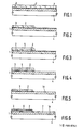
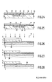
- FIGs 1 to 9 show diagrammatically in cross-section successive stages of an. embodiment of the method according to the invention.
- the starting material (see Figure 1) is a first silicon layer 1 on which an oxidation-preventing layer 3 is formed which consists, for example, of silicon nitride or silicon oxynitride.
- a second silicon layer 2 is formed on the layer 3.
- the assembly is provided on a substrate 4 which consists of an arbitrary material, for example insulating or semiconductor material.
- the silicon layers 1 and 2 are generally non-monocrystalline.
- the substrate 4 consists of monocrystalline semiconductor material
- the layer 1 may be under given circumstances a nonocrystalline epitaxial layer.
- both layers 1 and 2 consists of polycrystalline silicon, which by the use of known techniques is deposited, like the anti-oxidation layer 3, from the gaseous phase.
- the second silicon layer 2 (see Figure 2) is now removed in part, after which the remaining part of the layer 2 is oxidized in part and converted into silicon oxide 5 during a first oxidation step ( see Figure 3).
- the silicon layer 1 has a thickness of 0.5
- the silicon layer 2 has a thickness of 0.7 /um
- the intermediate layer 3 has a thickness of 0.1 /um and consists of silicon nitride.
- the said first oxidation step is effected at 1000°C in steam for 120 minutes.
- the non-oxidized part of the layer 2 after this oxidation has a thickness of about 0.45 /um and the oxide layer 5 has on the layer 2 a thickness of about 0.6 /um.
- the part of the oxidation-preventing layer 3 not covered by the oxidized second silicon layer (2,5) is selectively removed by etching in, for example, hot phosphoric acid, a first part 1A of the first silicon layer 1 being exposed; see Figure 4.
- the oxide 5 is then removed by etching in a solution of HF in water; see Figure 5.
- a small part of the layer 3 corresponding to the width of the oxidized edge 5 of the layer 2 then projects beneath the layer 2.
- a second oxidation step at a temperature between 700°C and 800°C, in this example at 750°C for 60 minutes. in steam, the exposed first part 1A of the first silicon layer 1 and the remaining part of the second silicon layer 2 are thermally oxidized, an oxide layer 6 being formed on the layer 2 and an oxide layer 7 being formed on the layer 1; see Figure 6.
- the oxide layer 7 becomes considerably thicker (about 150 nm)than the oxide layer 6 (about 15 nm).
- the uncovered part of the oxidation-preventing layer 3 is now selectively etched away (see Figure 7) in, for example, hot phosphoric acid, a narrow strip of the silicon layer 1 being exposed.
- the oxide layer 6 of the second silicon layer 2 is removed entirely and the thicker oxide layer 7 of the first silicon layer 1 is removed only in part; see Figure 8. This may be effected by, for example, dip-etching in a 1 % HF solution.
- a groove 8 is etched into the exposed part of the first seminconductor layer 1, for example, by selective etching in a chlorine plasma ( see Figure 9) which groove extends over the whole thickness or over only part of the thickness of the layer 1 and separates the first part 1A from the remaining second part 1B of the silicon layer 1.
- This etching process which is also carried out without a mask, in accordance with the invention is continued until the remaining part of the second silicon layer 2 has also disappeared.
- the width of the groove 8 is determined by the thickness of the oxide layer 5.
- Figures 1 to 9 the principle of the method according to the invention is illustrated, With the use of this method, a variety of semiconductor devices can be manufactured. Many variations can be used in carrying out the method. For example, one or more of the etching steps described may be carried out by means of plasma-etching.
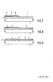
- Figures 10 to 16 show diagrammatically in cross-section successive stages in the manufacture of the electrode structure of a CCD or charge-coupled device by the use of the method according to the invention.
- the starting material (see Figure 10) is a p-type silicon substrate 4, on which an oxide layer 10 having a thickness of 70 nm is formed by thermal oxidation.
- the thickness of the layer 1 is, for example, 0.5 /um.
- a second silicon layer 2 which is undoped and has a thickness of, for example, 0.7 / um.
- This layer 2 is subdivided into strip-shaped parts by masking and etching, the edges of these parts approximately corresponding to the edges of the gate electrode structure to be ultimately formed. Thus, the situation shown in Figure 10 is obtained.
- a first thermal oxidation step is carried out at 10000C for 120 minutes in steam, a part of the silicon layer 2 being converted into the 0.6 /um thick silicon oxide layer 5; see Figure 11.
- the uncovered part of the silicon nitride or oxynitride layer 3 is then removed, after which the oxide 5 is removed in, for example, a HF solution in water.
- the oxide 5 is removed in, for example, a HF solution in water.
- a thin oxide layer 6 is now formed on the undoped silicon layer 2 and an about ten times thicker oxide layer 7 is formed on the heavily n-doped silicon layer 1; see Figure 13.
- the thicknesses of the layers 6 and 7 may be larger, for example 15 nm and 150 nm, respectively.
- the oxide layer 6 is etched away entirely and the oxide layer 7 is etched away only over part of its thickness by dip-etching in a 1 % hydrofluoride solution. After the uncovered parts of the nitride layer 3 have been selectively etched away also without a mask, the situation shown in Figure 14 is obtained.
- the first silicon layer 1 is etched away over its whole thickness down to the oxide 10. This may be effected by plasma-etching, for example in a chlorine plasma.
- the remaining part of the second silicon layer 2 then also disappears so that the structure shown in Figure 15 is obtained comprising a number of strip-shaped silicon electrodes which are located very closely to each other, are separated from each other by grooves 8 and are covered alternately (1B) by nitride 3 or (1A) by oxide 7.
- the intermediate space between the electrodes is determined by the thickness of the oxide layer 5.
- source and drain zones S and D with a high n-type doping may be formed at the ends of the electrode structure by means of ion implantation.
- the oxide layer 6 may be removed in, for example, a CC14 (carbon tetrachloride) plasma and then the step of etching the silicon layer 1 may be continued and completed in a chlorine plasma whilst simultaneously etching away the remaining silicon layer 2.
- a CC14 carbon tetrachloride
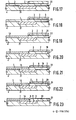
- the method according to the invention is also particularly suitable for the manufacture of bipolar semiconductor devices, for example small bipolar transistors having closely adjacent base and emitter connections. An example thereof will be described with reference to Figures 17 to 25.
- a thermal oxide layer 20 into which a window is etched; see Figure 17.
- a base zone 21 is diffused or inplanted.
- a first undoped silicon layer 1 is now deposited in a usual manner from the gaseous phase on the substrate 4 covered partly by the oxide layer 20 and comprising the base zone 21.
- This silicon layer 2 is removed in part by masking and etching, the edge of the remaining part of the layer 2 being located inside the window in the oxide layer 20.
- the situation shown in Figure 17 is obtained.
- the layer 2 is provided with a 0.6 /um thick oxide layer 5, after which the exposed part of the nitride layer 3 is etched away without masking whilst using the oxidized silicon layer (2,5) as a mask; see Figure 18.
- the exposed part 1A of the layer 1 is then heavily n-doped (doping 7. 10 20 atoms/cm 3 ). In this example, this is effected by implantation of phosphorus or arsenic ions.
- the oxide layer 5 then serves as a mask so that the subjacent layer 2 and the part 1A of the layer 1 are not doped; see Figure 19.
- the oxide 5 is then removed in a H F solution; see Figure 20.
- a second oxidation step at 750°C in steam for 60 minutes, a thin oxide layer 6 about 15 nm thick is formed on the undoped second silicon layer 2 and a thicker oxide layer 7 about 150 nm thick is formed on the exposed heavily n-doped first part 1A of the first silicon layer 1; see Figure 21.
- the uncovered part of the oxidation-preventing layer 3 is now selectively removed by etching; see Figure 22.
- etching By dip-etching in a 1 % HF solution the thin oxide layer 6 is then removed, the thicker oxide layer 7 being attacked only superficially.
- etching in, for example, a chlorine plasma, a groove 8 is then etched into the layer 1 (see Figure 23), which groove separates the first part 1A from the remaining second part 1B.
- the groove 8 extends over the whole thickness of the layer 1 into the base zone 21.
- the remaining part of the second silicon layer 2 then also disappears.
- a third thermal oxidation step is carried out at 1000 0 C for 30 minutes in steam resulting in the layer 1A and the wall and bottom of the groove 8 being covered by an oxide layer 23; see Figure 24.
- the nitride layer 3 is etched away selectively, after which the part 1B of the silicon layer 1 is rendered strongly p-tyre conducting (doping 5.10 19 atoms/cm 3 ) by implantation of boron ions.
- a p-type base contact zone 24 may then also be formed; see Figure 25.
- a transistor of very small dimensions is obtained, the distance between the emitter connection 1A and the base connection 1B being determined by the thickness of the oxide layer 5.
- the invention is not restricted to the embodiments described above.
- many other semiconductor devices than those described here may be manufactured by means of the method according to the invention.
- the oxidation-preventing layer may consists of materials other than silicon nitride or silicon oxynitride. More particularly, in order to prevent lattice defects, a silicon nitride layer with an underlying thin silicon oxide layer be used. Inter alia in order to prevent underetching problems, in this case a slightly different method may be used in order of succession of Figures 1 to 9, starting from Figure 3. This will be illustrated with reference to Figures 26 to 28.
- Figure 26 corresponds to Figure 3, but in this case a thin silicon oxide layer 30 is provided between the silicon nitride layer 3 (which is shown with a larger thickness for the sake of clarity) and the silicon layer 1.
- a bombadment with energetic particles, for example nitrogen ions, in the direction of the arrows 31 ensures that the bombarded nitride (indicated in dotted lines in Figure 26) can be etched more rapidly.
- the oxide 5 masks against this bombardment. After etching away the oxide 5 ( Figure 27) the exposed nitride is etched in hot phosphoric acid.
Landscapes
- Engineering & Computer Science (AREA)
- Manufacturing & Machinery (AREA)
- Physics & Mathematics (AREA)
- Condensed Matter Physics & Semiconductors (AREA)
- General Physics & Mathematics (AREA)
- Computer Hardware Design (AREA)
- Microelectronics & Electronic Packaging (AREA)
- Power Engineering (AREA)
- Inorganic Chemistry (AREA)
- Chemical & Material Sciences (AREA)
- Element Separation (AREA)
- Bipolar Transistors (AREA)
- Solid State Image Pick-Up Elements (AREA)
- Local Oxidation Of Silicon (AREA)
Applications Claiming Priority (2)
| Application Number | Priority Date | Filing Date | Title |
|---|---|---|---|
| NL8302541 | 1983-07-15 | ||
| NL8302541A NL8302541A (nl) | 1983-07-15 | 1983-07-15 | Werkwijze ter vervaardiging van een halfgeleiderinrichting, en halfgeleiderinrichting vervaardigd volgens de werkwijze. |
Publications (3)
| Publication Number | Publication Date |
|---|---|
| EP0132009A2 true EP0132009A2 (de) | 1985-01-23 |
| EP0132009A3 EP0132009A3 (en) | 1985-03-13 |
| EP0132009B1 EP0132009B1 (de) | 1987-04-22 |
Family
ID=19842167
Family Applications (1)
| Application Number | Title | Priority Date | Filing Date |
|---|---|---|---|
| EP84201019A Expired EP0132009B1 (de) | 1983-07-15 | 1984-07-11 | Verfahren zur Herstellung einer Halbleiteranordnung und nach diesem Verfahren hergestellte Halbleiteranordnung |
Country Status (7)
| Country | Link |
|---|---|
| US (2) | US4659428A (de) |
| EP (1) | EP0132009B1 (de) |
| JP (1) | JPS6038874A (de) |
| CA (1) | CA1216969A (de) |
| DE (1) | DE3463317D1 (de) |
| IE (1) | IE55653B1 (de) |
| NL (1) | NL8302541A (de) |
Cited By (6)
| Publication number | Priority date | Publication date | Assignee | Title |
|---|---|---|---|---|
| EP0158371A1 (de) * | 1984-01-25 | 1985-10-16 | Koninklijke Philips Electronics N.V. | Verfahren zur Herstellung einer Halbleiteranordnung und nach diesem Verfahren hergestellte Anordnung |
| EP0171105A3 (en) * | 1984-07-13 | 1986-02-19 | N.V. Philips' Gloeilampenfabrieken | Method of manufacturing a semiconductor device and device manufactured by the use of the method |
| EP0181812A1 (de) * | 1984-11-06 | 1986-05-21 | Thomson-Csf | Verfahren zu einer Gate-Struktur für integrierte Schaltungen |
| WO1988005603A1 (fr) * | 1987-01-26 | 1988-07-28 | Commissariat A L'energie Atomique | Procede de fabrication des zones d'isolation electrique d'un circuit integre cmos |
| EP0409132A3 (en) * | 1989-07-21 | 1991-11-21 | Motorola Inc. | Method of fabricating a structure having self-aligned diffused junctions |
| EP0412263A3 (en) * | 1989-08-10 | 1993-01-07 | Kabushiki Kaisha Toshiba | Method of forming a contact hole in semiconductor integrated circuit |
Families Citing this family (19)
| Publication number | Priority date | Publication date | Assignee | Title |
|---|---|---|---|---|
| NL8302541A (nl) * | 1983-07-15 | 1985-02-01 | Philips Nv | Werkwijze ter vervaardiging van een halfgeleiderinrichting, en halfgeleiderinrichting vervaardigd volgens de werkwijze. |
| US5067002A (en) * | 1987-01-30 | 1991-11-19 | Motorola, Inc. | Integrated circuit structures having polycrystalline electrode contacts |
| US4837176A (en) * | 1987-01-30 | 1989-06-06 | Motorola Inc. | Integrated circuit structures having polycrystalline electrode contacts and process |
| US5092957A (en) * | 1989-11-24 | 1992-03-03 | The United States Of America As Represented By The United States Department Of Energy | Carrier-lifetime-controlled selective etching process for semiconductors using photochemical etching |
| US5240512A (en) * | 1990-06-01 | 1993-08-31 | Texas Instruments Incorporated | Method and structure for forming a trench within a semiconductor layer of material |
| US5120675A (en) * | 1990-06-01 | 1992-06-09 | Texas Instruments Incorporated | Method for forming a trench within a semiconductor layer of material |
| JPH04212472A (ja) * | 1990-07-13 | 1992-08-04 | Toshiba Corp | 不揮発性半導体記憶装置の製造方法 |
| US5026665A (en) * | 1990-12-24 | 1991-06-25 | Motorola Inc. | Semiconductor device electrode method |
| US5305519A (en) * | 1991-10-24 | 1994-04-26 | Kawasaki Steel Corporation | Multilevel interconnect structure and method of manufacturing the same |
| US5292680A (en) * | 1993-05-07 | 1994-03-08 | United Microelectronics Corporation | Method of forming a convex charge coupled device |
| US5968058A (en) * | 1996-03-27 | 1999-10-19 | Optonol Ltd. | Device for and method of implanting an intraocular implant |
| US6203513B1 (en) | 1997-11-20 | 2001-03-20 | Optonol Ltd. | Flow regulating implant, method of manufacture, and delivery device |
| US8313454B2 (en) * | 1997-11-20 | 2012-11-20 | Optonol Ltd. | Fluid drainage device, delivery device, and associated methods of use and manufacture |
| US6558342B1 (en) | 1999-06-02 | 2003-05-06 | Optonol Ltd. | Flow control device, introducer and method of implanting |
| US6770904B2 (en) * | 2002-01-11 | 2004-08-03 | Xerox Corporation | Polythiophenes and electronic devices generated therefrom |
| JP4347009B2 (ja) * | 2003-09-26 | 2009-10-21 | キヤノン株式会社 | 近接場光の発生方法、近接場露光用マスク、近接場露光方法、近接場露光装置、近接場光ヘッド |
| US7862531B2 (en) * | 2004-06-25 | 2011-01-04 | Optonol Ltd. | Flow regulating implants |
| US8109896B2 (en) * | 2008-02-11 | 2012-02-07 | Optonol Ltd. | Devices and methods for opening fluid passageways |
| JP6667410B2 (ja) * | 2016-09-29 | 2020-03-18 | 東京エレクトロン株式会社 | ハードマスクおよびその製造方法 |
Family Cites Families (6)
| Publication number | Priority date | Publication date | Assignee | Title |
|---|---|---|---|---|
| US3767492A (en) * | 1971-10-12 | 1973-10-23 | Bell Telephone Labor Inc | Semiconductor masking |
| US4053349A (en) * | 1976-02-02 | 1977-10-11 | Intel Corporation | Method for forming a narrow gap |
| EP0051534B1 (de) * | 1980-10-29 | 1986-05-14 | FAIRCHILD CAMERA & INSTRUMENT CORPORATION | Selbstjustierendes Verfahren zur Herstellung integrierter Stromkreisstrukturen unter Verwendung unterschiedlicher Oxydationsraten |
| NL8105559A (nl) * | 1981-12-10 | 1983-07-01 | Philips Nv | Werkwijze voor het aanbrengen van een smalle groef in een substraatgebied, in het bijzonder een halfgeleidersubstraatgebied. |
| NL8202686A (nl) * | 1982-07-05 | 1984-02-01 | Philips Nv | Werkwijze ter vervaardiging van een veldeffektinrichting met geisoleerde stuurelektrode, en inrichting vervaardigd volgens de werkwijze. |
| NL8302541A (nl) * | 1983-07-15 | 1985-02-01 | Philips Nv | Werkwijze ter vervaardiging van een halfgeleiderinrichting, en halfgeleiderinrichting vervaardigd volgens de werkwijze. |
-
1983
- 1983-07-15 NL NL8302541A patent/NL8302541A/nl not_active Application Discontinuation
-
1984
- 1984-07-11 CA CA000458637A patent/CA1216969A/en not_active Expired
- 1984-07-11 EP EP84201019A patent/EP0132009B1/de not_active Expired
- 1984-07-11 DE DE8484201019T patent/DE3463317D1/de not_active Expired
- 1984-07-12 JP JP59143407A patent/JPS6038874A/ja active Pending
- 1984-07-12 IE IE1792/84A patent/IE55653B1/en unknown
-
1986
- 1986-03-17 US US06/840,164 patent/US4659428A/en not_active Expired - Fee Related
-
1987
- 1987-01-27 US US07/007,152 patent/US4750971A/en not_active Expired - Fee Related
Cited By (10)
| Publication number | Priority date | Publication date | Assignee | Title |
|---|---|---|---|---|
| EP0158371A1 (de) * | 1984-01-25 | 1985-10-16 | Koninklijke Philips Electronics N.V. | Verfahren zur Herstellung einer Halbleiteranordnung und nach diesem Verfahren hergestellte Anordnung |
| EP0171105A3 (en) * | 1984-07-13 | 1986-02-19 | N.V. Philips' Gloeilampenfabrieken | Method of manufacturing a semiconductor device and device manufactured by the use of the method |
| EP0181812A1 (de) * | 1984-11-06 | 1986-05-21 | Thomson-Csf | Verfahren zu einer Gate-Struktur für integrierte Schaltungen |
| FR2573919A1 (fr) * | 1984-11-06 | 1986-05-30 | Thomson Csf | Procede de fabrication de grilles pour circuit integre |
| US4738683A (en) * | 1984-11-06 | 1988-04-19 | Thomson-Csf | Method of fabrication of gates for integrated circuits |
| WO1988005603A1 (fr) * | 1987-01-26 | 1988-07-28 | Commissariat A L'energie Atomique | Procede de fabrication des zones d'isolation electrique d'un circuit integre cmos |
| FR2610140A1 (fr) * | 1987-01-26 | 1988-07-29 | Commissariat Energie Atomique | Circuit integre cmos et procede de fabrication de ses zones d'isolation electrique |
| US4889828A (en) * | 1987-01-26 | 1989-12-26 | Commissiriat A L'energie Atomique | Process for the production of electrical isolation zones in a CMOS integrated circuit |
| EP0409132A3 (en) * | 1989-07-21 | 1991-11-21 | Motorola Inc. | Method of fabricating a structure having self-aligned diffused junctions |
| EP0412263A3 (en) * | 1989-08-10 | 1993-01-07 | Kabushiki Kaisha Toshiba | Method of forming a contact hole in semiconductor integrated circuit |
Also Published As
| Publication number | Publication date |
|---|---|
| DE3463317D1 (en) | 1987-05-27 |
| US4659428A (en) | 1987-04-21 |
| CA1216969A (en) | 1987-01-20 |
| IE55653B1 (en) | 1990-12-05 |
| NL8302541A (nl) | 1985-02-01 |
| IE841792L (en) | 1985-01-15 |
| US4750971A (en) | 1988-06-14 |
| JPS6038874A (ja) | 1985-02-28 |
| EP0132009B1 (de) | 1987-04-22 |
| EP0132009A3 (en) | 1985-03-13 |
Similar Documents
| Publication | Publication Date | Title |
|---|---|---|
| EP0132009B1 (de) | Verfahren zur Herstellung einer Halbleiteranordnung und nach diesem Verfahren hergestellte Halbleiteranordnung | |
| US4477310A (en) | Process for manufacturing MOS integrated circuit with improved method of forming refractory metal silicide areas | |
| EP0066081B1 (de) | Vertikaler Feldeffekttransistor mit grosser Dichtheit und Verfahren zu dessen Herstellung | |
| EP0122662B1 (de) | Verfahren zur Herstellung einer Halbleiteranordnung unter Verwendung der Herstellung einer Struktur in einer Siliciumnitridschicht mittels einer Ionenimplantation | |
| EP0137645B1 (de) | Verfahren zur Bildung eines seichten Gebietes des N-Typs | |
| EP0227085A2 (de) | Verfahren zum Herstellen von IGFETs mit minimaler Übergangstiefe durch epitaktische Rekristallisation | |
| EP0034910A1 (de) | Verfahren zur Herstellung einer Halbleitervorrichtung und so hergestellte Vorrichtung | |
| EP0229362B1 (de) | Halbleitervorrichtung und Methode zur Herstellung | |
| US4168999A (en) | Method for forming oxide isolated integrated injection logic semiconductor structures having minimal encroachment utilizing special masking techniques | |
| US4640721A (en) | Method of forming bipolar transistors with graft base regions | |
| EP0242746A1 (de) | Herstellungsverfahren einer integrierten Schaltung | |
| US4408387A (en) | Method for producing a bipolar transistor utilizing an oxidized semiconductor masking layer in conjunction with an anti-oxidation mask | |
| US4402128A (en) | Method of forming closely spaced lines or contacts in semiconductor devices | |
| EP0051534B1 (de) | Selbstjustierendes Verfahren zur Herstellung integrierter Stromkreisstrukturen unter Verwendung unterschiedlicher Oxydationsraten | |
| EP0052038B1 (de) | Herstellungsverfahreneiner integrierten Schaltkreisstruktur | |
| JPH025432A (ja) | 半導体装置の製造方法 | |
| KR880000483B1 (ko) | 반도체소자의 제조방법 | |
| JP2743894B2 (ja) | 半導体装置の製造方法 | |
| KR0124642B1 (ko) | 반도체 소자의 제조방법 | |
| KR0172260B1 (ko) | 반도체 소자의 코발트 실리사이드 형성방법 | |
| JP2812298B2 (ja) | バイポーラトランジスタの製造方法 | |
| KR0124634B1 (ko) | 반도체소자의 분리층 제조방법 | |
| JP2546650B2 (ja) | バイポ−ラトランジスタの製造法 | |
| JPS5968950A (ja) | 半導体装置の製造方法 | |
| JPH02304931A (ja) | 半導体装置及びその製造方法 |
Legal Events
| Date | Code | Title | Description |
|---|---|---|---|
| PUAI | Public reference made under article 153(3) epc to a published international application that has entered the european phase |
Free format text: ORIGINAL CODE: 0009012 |
|
| PUAL | Search report despatched |
Free format text: ORIGINAL CODE: 0009013 |
|
| AK | Designated contracting states |
Designated state(s): CH DE FR GB IT LI NL |
|
| AK | Designated contracting states |
Designated state(s): CH DE FR GB IT LI NL |
|
| 17P | Request for examination filed |
Effective date: 19850802 |
|
| 17Q | First examination report despatched |
Effective date: 19860704 |
|
| GRAA | (expected) grant |
Free format text: ORIGINAL CODE: 0009210 |
|
| AK | Designated contracting states |
Kind code of ref document: B1 Designated state(s): CH DE FR GB IT LI NL |
|
| REF | Corresponds to: |
Ref document number: 3463317 Country of ref document: DE Date of ref document: 19870527 |
|
| ITF | It: translation for a ep patent filed | ||
| ET | Fr: translation filed | ||
| PLBE | No opposition filed within time limit |
Free format text: ORIGINAL CODE: 0009261 |
|
| STAA | Information on the status of an ep patent application or granted ep patent |
Free format text: STATUS: NO OPPOSITION FILED WITHIN TIME LIMIT |
|
| 26N | No opposition filed | ||
| PGFP | Annual fee paid to national office [announced via postgrant information from national office to epo] |
Ref country code: GB Payment date: 19900702 Year of fee payment: 7 |
|
| PGFP | Annual fee paid to national office [announced via postgrant information from national office to epo] |
Ref country code: FR Payment date: 19900720 Year of fee payment: 7 |
|
| ITTA | It: last paid annual fee | ||
| PGFP | Annual fee paid to national office [announced via postgrant information from national office to epo] |
Ref country code: NL Payment date: 19900731 Year of fee payment: 7 |
|
| PGFP | Annual fee paid to national office [announced via postgrant information from national office to epo] |
Ref country code: DE Payment date: 19900921 Year of fee payment: 7 |
|
| PGFP | Annual fee paid to national office [announced via postgrant information from national office to epo] |
Ref country code: CH Payment date: 19901024 Year of fee payment: 7 |
|
| PG25 | Lapsed in a contracting state [announced via postgrant information from national office to epo] |
Ref country code: GB Effective date: 19910711 |
|
| PG25 | Lapsed in a contracting state [announced via postgrant information from national office to epo] |
Ref country code: LI Effective date: 19910731 Ref country code: CH Effective date: 19910731 |
|
| PG25 | Lapsed in a contracting state [announced via postgrant information from national office to epo] |
Ref country code: NL Effective date: 19920201 |
|
| GBPC | Gb: european patent ceased through non-payment of renewal fee | ||
| NLV4 | Nl: lapsed or anulled due to non-payment of the annual fee | ||
| PG25 | Lapsed in a contracting state [announced via postgrant information from national office to epo] |
Ref country code: FR Effective date: 19920331 |
|
| REG | Reference to a national code |
Ref country code: CH Ref legal event code: PL |
|
| PG25 | Lapsed in a contracting state [announced via postgrant information from national office to epo] |
Ref country code: DE Effective date: 19920401 |
|
| REG | Reference to a national code |
Ref country code: FR Ref legal event code: ST |