EP0124900A2 - Circuit de mémoire, de type à redondance, ayant un générateur d'horloge amélioré - Google Patents
Circuit de mémoire, de type à redondance, ayant un générateur d'horloge amélioré Download PDFInfo
- Publication number
- EP0124900A2 EP0124900A2 EP84105145A EP84105145A EP0124900A2 EP 0124900 A2 EP0124900 A2 EP 0124900A2 EP 84105145 A EP84105145 A EP 84105145A EP 84105145 A EP84105145 A EP 84105145A EP 0124900 A2 EP0124900 A2 EP 0124900A2
- Authority
- EP
- European Patent Office
- Prior art keywords
- circuit
- array
- memory
- redundant
- timing
- Prior art date
- Legal status (The legal status is an assumption and is not a legal conclusion. Google has not performed a legal analysis and makes no representation as to the accuracy of the status listed.)
- Granted
Links
Images


Classifications
-
- G—PHYSICS
- G11—INFORMATION STORAGE
- G11C—STATIC STORES
- G11C29/00—Checking stores for correct operation ; Subsequent repair; Testing stores during standby or offline operation
- G11C29/70—Masking faults in memories by using spares or by reconfiguring
- G11C29/78—Masking faults in memories by using spares or by reconfiguring using programmable devices
- G11C29/84—Masking faults in memories by using spares or by reconfiguring using programmable devices with improved access time or stability
- G11C29/842—Masking faults in memories by using spares or by reconfiguring using programmable devices with improved access time or stability by introducing a delay in a signal path
Definitions
- the present invention relates to memory circuits, and more specifically to redundant type memory circuits having redundant structure.
- the memory capacity of semiconductor memories has been recently increased, but the increase in the memory capacity has resulted in low fabrication yield due to the low probability of all circuit elements on such a dense structure being fabricated without defect. Hence, it has become difficult to obtain a memory in which all the constituent elements are good.
- a redundant array of memory cells is provided in addition to a normal array of memory cells. If a cell or cells in the normal array are faulty or defective, such defective cells are functionally replaced by good cells in the redundant array, so that a functionally good memory can be obtained even though defects may be present in the normal array.
- the replacement of a defective cell in the normal array with a good cell in the redundant array is typically conducted by replacing a column or a row including the defective cell in the normal array with a column or a row of good cells in the redundant array.
- a programmable type redundant decoder circuit is provided to the redundant array to operatively select columns or rows of the redundant array. Information as to the address of the replaced columns or rows is stored by the programmable type redundant decoder.
- the programmable type redundant decoder circuit operates to select one column or one row in the redundant array while accessing of the defective column or defective row in the normal array is inhibited by an inhibit signal which is generated in response to a selection output of the redundant decoder circuit. Namely, when the redundant cell array is accessed by the redundant decoder, a normal decoder circuit provided to the normal array is inhibited from selecting the normal array.
- the redundant decoder circuit is first activated, and then the normal decoder is activated only when the any column or row in the redundant array is not selected by the redundant decoder circuit, and the inhibit signal is not generated. Therefore, a clock generator employed in the redundant type memory is designed to generate a first clock for enabling the redundant decoder circuit, and thereafter generate a second clock for enabling the normal decoder circuit.
- the redundant decoder circuit is programmed not to select the redundant array
- the activation of the normal decoder circuit is still performed by the second clock which is generated with a delayed time from the occurrence of the first clock, and hence operation of the memory is unnecessarily delayed, resulting in a low speed operation.
- a memory circuit is of the type having a normal array of memory cells, a redundant array of memory cells, a normal decoder circuit provided to the normal array of memory cells, a programmable redundant decoder circuit provided to the redundant array, a detection circuit for detecting that the redundant decoder circuit accesses the redundant array, a control circuit for inhibiting the operation of the normal decoder circuit when the detection circuit detects the access by the redundant decoder circuit, and a clock generator responsive to a control signal for generating a first clock for enabling the redundant decoder circuit and a second clock for enabling the normal decoder circuit after generation of the first clock, and is featured that a delay time from the activation of the control signal to the generation of the second clock is variable.
- the program means is programmed so as to set the delay time at a large value.
- the program means is programmed so as to set the delay time at a small value.
- the second clock is generated with the minimum delay time so that the normal array can be accessed at the maximum speed.
- the second clock is generated with such delay time that the normal decoder circuit is enabled after the activation of the redundant decoder circuit.
- the time point when the normal decoder circuit starts its operation need not be delayed when the redundant array is not used even with the memory having the redundant array, and the time point when the normal decoder circuit starts its operation is delayed so as to allow the redundant decoder circuit to operate prior to the normal decoder circuit.
- the present invention when the memory has no defective cell in the normal array, a high speed operation can be obtained without increasing manufacturing steps and changing any circuit structure.
- a redundant memory cell array is provided in such manner that a defective row (e.g., a defective word line) coupled to the faulty memory cell is replaced by a good row of the redundant memory cell array.
- a defective row e.g., a defective word line
- a normal memory cell array 20 includes a plurality of memory cells MC arranged at intersections of word lines WL arrayed in rows and digit lines DL arrayed in columns.
- the word lines WL of the normal memory cell array 20 are connected to output terminals of a normal decoder circuit 11 in one by one relation.
- a redundant memory cell array 21 includes a plurality of redundant memory cells MC' arranged at intersections of redundant word lines RWL and the digit lines DL.
- the redundant word lines RWL are connected to output terminals of a programmable type redundant decoder circuit 30.
- An address buffer circuit 10 receives plural bit address signals AS and generates their true and complementary signals. The true and complementary address signals are applied to the redundant decoder circuit 30 and to the normal decoder.
- An inhibit control circuit is coupled to the outputs of the redundant decoder circuit to operatively inhibit the normal decoder circuit from operating when one of outputs of the redundant decoder circuit takes a selection level.
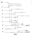
- a clock generator circuit includes delay circuits 1 to 4 connected in cascade. The delay circuit 1 receives a row strobe signal RAS and generates a first clock signal ⁇ 1 for enabling the address buffer circuit 10. The delay circuit 2 generates a second clock signal ⁇ 2 in response to the clock signal ⁇ 1 for enabling the redundant decoder circuit 30. The delay circuit 3 generates a third clock signal ⁇ 3 in response to the second clock signal ⁇ 2 for enabling the inhibit control circuit 31. The delay circuit 4 generates a fourth clock signal ⁇ 4 in response to the third clock signal ⁇ 3 for enabling the normal decoder 11.
- the redundant decoder circuit 30 is programmed in such a manner that, when contents of the true and complementary address signals from the address buffer circuit 10 correspond to an address of a defective word line WL coupled to the defective memory cell in the normal memory cell array, the redundant decoder circuit 30 selects one of good redundant word lines RWL.
- the delay circuit 1 in response to an active level of the strobe signal RAS, the delay circuit 1 generates the first clock signal ⁇ 1 .
- the address buffer circuit 10 is enabled by the clock ⁇ 1 , so that the address buffer circuit 10 generates a plural bit true and complementary address signals (Ai, Ai) and holds them.
- the redundant decoder circuit is enabled in response to the occurrence of the second clock signal $ 2 .
- the redundant decoder circuit 30 operates to select one good redundant word line RWL.
- the redundant decoder 30 selects no redundant word line RWL.
- the inhibit control circuit 31 is enabled by the third clock signal ⁇ 3 .
- the inhibit control circuit 31 when the redundant decoder circuit 30 has been selecting one of the redundant word lines RWL, the inhibit control circuit 31 generates an inhibit signal 31'.
- the inhibit control circuit 31 does not produce the inhibit signal 31'.
- the normal decoder circuit 11 In response to the occurrence of the fourth clock signal ⁇ 4 , the normal decoder circuit 11 is enabled. However, in this instance, if the inhibit control circuit 31 has been producing the inhibit signal 31', the normal decoder circuit 11 does not select any-one of the word lines WL. On the other hand, if the inhibit control circuit 31 has not been producing the inhibit signals 31', the normal decoder circuit 11 selects one of the word lines WL in the normal memory array 20. However, even the case where all of the elements of the normal memory cell array are perfectly good and the redundant memory cell array is not used, the normal decoder circuit 11 cannot operate until the time point when the fourth clock signal ⁇ 4 is generated. Therefore, unnecessary delay time is inevitably present from the operation of the address buffer circuit 10 to the operation of the normal decoder circuit 11, resulting a low speed operation.
- Fig. 3 shows a major part of the memory circuit according to the present invention.
- components corresponding to those in Fig. 1 are designated by similar reference numerals.
- This embodiment is obtained by replacing the clock generator CG of Fig. 1 with a programmable type clock generator CG' as shown in Fig. 3.
- a programmable delay circuit PD is employed.
- the programmable delay circuit PD includes a multi-input delay circuit 4' having one input terminal a coupled to the output of the delay circuit 3 and another input terminal b coupled to the output terminal of the delay circuit 1 through a fusible link 40 as to a programmable element.
- the multi-input delay circuit 4' generates an output to serve as the clock signal ⁇ 4 ', the output ⁇ 4 ' corresponding to an OR logic combination of the input signals at the input terminals a and b.
- the delay circuit produces the output signal ⁇ 4 ' in response to the occurrence of the first clock signal ⁇ 1 . Therefore, the signal ⁇ 4 ' takes an active level with only a short delay time after the occurrence of the clock ⁇ 1 .
- the delay circuit 4' is no longer sensitive to the first clock signal ⁇ 1 but instead produces the output signal ⁇ 4 ' only in response to the occurrence of the clock signal ⁇ 3 . The signal ⁇ 4 ' then takes the active level with a large delay time after the occurrence of the clock signal ⁇ 1 .
- the programming of the fusible link 40 is conducted as follows: When all functional elements in the normal memory cell array 20 are good, the fusible link 40 is uncut. On the contrary, when the normal memory cell array 20 includes at least one defective element to be replaced with good one from the redundant memory cell array 21, the fusible link 40 is cut.
- the fusible link 40 is uncut.
- the row address strobe signal RAS changes to its active level, i.e., a low level
- the first clock signal ⁇ 1 changes from the low level to a high level.
- the address buffer circuit 10 develops plural bit true and complementary address signals (Ai, Ai) indicated as 10' in Fig. 4.
- the clock signal ⁇ 4 ' changes from the low level to the high level after a short delay time T has elapsed.
- the delay time T is provided to ensure completion of the operation of the address buffer circuit 10 prior to the operation of the normal decoder circuit 11.
- the normal decoder circuit 11 performs the selection operation of the normal memory cell array 20. As a result of the selection operation, one of the output terminals of the normal decoder circuit 11 is switched to a high level while the remaining outputs are unselected and are maintained at a low level. Thus, accessing of the word line WL of the normal memory cell array is accomplished.
- the delay circuit 2 and 3 generate the second and third clock signals ⁇ 2 and ⁇ 3 , respectively.
- the redundant decoder circuit 30 is programmed in such a manner that all output terminals (30') of the redundant decoder circuit 30 remain at a non-selected level.
- the inhibit control circuit 31 does not generate the inhibit signal 31' even when the third clock signal ⁇ 3 is applied thereto, because no redundant word line RWL has been selected. Therefore, the delay circuits 2 and 3, the redundant decoder circuit 30, and the inhibit control circuit 31 do not affect the operation of accessing the normal memory cell array 20.
- the fusible link 40 is cut and the delay circuit 4' will be responsive only to the third clock signal ⁇ 3 . Accordingly, the delay circuit 4' produces the fourth clock signal ⁇ 4 ' after the occurrence of thesignal ⁇ 3 .
- the memory circuit of this embodiment operates in the same manner as the circuit shown in Fig. 1, and the clock signal ⁇ 4 ' has the same waveform as that of in Fig. 2.
- Fig. 5 shows a unit structure 10 i of the address buffer circuit 10.
- the unit structure 10 i is composed of a flip-flop circuit 100 receiving one bit Ai of the address input at its input terminal and the clock signal ⁇ 1 at its clock terminal CL. When the clock signal ⁇ 1 is activated,
- the address buffer circuit 10 includes the same number of the unit circuits 10. as the number of address bits.
- Fig. 6 shows one unit circuit structure 30 i for one redundant word line in the programmable redundant decoder circuit 30.
- the unit 30 i of the redundant decoder includes a programmable type NOR circuit composed of a precharge transistor Q 71 coupled between a power voltage terminal Vcc and a node N l, and a plurality of input transistors Q 72a , Q 72b ..., Q 75a' Q 75b receiving respective ones of the true and complementary signals from the buffer circuit 10 at their gates.
- the transistors Q 72 to Q75 are connected to the node N1 via fusible links 72a, 72b ... 75a, 75b, respectively.
- the node Nl is connected to a node N2 via a transistor Q 76 wnose gate is biased by the power voltage Vcc.
- a transistor Q 77 has a gate coupled to the node N2, a drain adapted to receive the clock signal ⁇ 2 and a source connected to an output line 30 . to be connected to one of the redundant word lines RWLi.
- a reset transistor Q 78 is connected between the source of the transistor Q 77 and ground potential.
- this unit circuit 30 i when the redundant word line RWLi is not needed to replace the word line WL of the normal memory cell array 20, all of the fusible links 72a, 72b ... 75a, 75b remain uncut.
- the redundant word line RWLi connected to this unit circuit 30 i is to replace the defective word line WL, the fusible links 72a, 72b ... 75a, 75b are selectively cut in such a manner that, when the contents of the address signals correspond to the defective word line WL in the normal memory cell array 20, the potential at the node Nl is kept at the high level.
- the fusible links coupled to the input transistors receiving the address signals A 0 , A 1 , A 2 , A3, A4 and A 5 cut while the fusible links coupled to the input transistors receiving the address signals A 0 , A 1 , A 2 , A 3 , A 4 and A 5 remain uncut.
- the fusible link associated with either the true or complementary address signal bit is cut while the other fusible link is left uncut.
- the fusible links 72 to 75 are typically made of polycrystalline silicon formed on a semiconductor substrate.
- a precharge control signal ⁇ p for controlling the transistors Q 71 and Q 78 is activated when the row strobe signal RAS is inactive level and inactivated when the row strobe signal RAS is made activated.
- Operation of this circuit 30 i is as follows. First, in response to the active level of the precharge control signal ⁇ p , the transistors Q 71 and Q 78 become conducting to precharge the node N1 with the power voltage and set the output line 30 i at ground potential. Then, the logic levels at nodes N1 and N2 will be determined by the states of the address signals A 0 , A 0 ... An, A n . Next, in response to the clock signal ⁇ 2 , the transistor Q 77 drives the redundant word line RWLi only when the nodes Nl and N2 are at the high level.
- Fig. 7 shows one example of circuitry for the inhibit control circuit 31.
- transistors Q 79 . . . Q 81 receiving the outputs 30 1 ' ... 30 n ' of the redundant decoder circuit 30 at their gates form an OR gate with a reset transistor Q 82 controlled by the precharge control signal ⁇ p .
- An output node N3 of the above OR gate is connected to a gate (N 4 ) of a transistor Q 84 via a drain- source path of a transistor Q 83 whose gate is biased by the power voltage Vcc.
- the transistor Q 84 has a drain receiving the clock signal ⁇ 3 and a source serving as the output 31' of the circuit 31.
- a transistor Q 85 is connected between the output 31' and ground potential to reset the output 31' in response to the reset signal ⁇ P .
- Fig. 8 shows a unit circuit structure 11 i for one word line in the normal decoder circuit 11.
- Transistors Q 86 , Q 87 ... Q 89 form a NOR gate together with a precharge transistor Q 90 in a known manner.
- the transistors Q 87 , Q 88 . . . Q 89 receive their associating true and complementary address signals (A 0 / A 0 ) ... (Ai/ Ai ) ... (An/ An ) in the same manner as the conventional decoder.
- the transistor Q 86 receiving the inhibit control signal 31' is added in parallel with the transistors Q 87 to Q 89 .
- the node N5 is connected via transistor Q 91 to a gate of a drive transistor Q 92 .
- the transistor Q 92 has a drain receiving the clock signal ⁇ 4 ' and a source serving as an output 11 i ' to be connected to one of the word lines WLi.
- a reset transistor Q 93 is connected between the output 11 i ' and ground potential.
- the circuit 11 i ' When the inhibit control signal 31' is at a low level, the circuit 11 i ' operates in the same manner as the conventional decoder. However, when the inhibit control signal 31' is at a high level, the level of the node N5 becomes low (ground level) irrespective of the states of the transistors Q 87 to Q 89 so that the selection of the word line Wli is inhibited.
- Fig. 9 shows one example of circuitry for the delay circuit 4' in Fig. 2.
- a series circuit of a transistor Q 94 having a gate connected to the input b and a transistor Q 95 having a gate receiving the precharge control signal ⁇ p serves as a buffer circuit for receiving the clock signal ⁇ 1 .
- a transistor Q 97 having a gate connected to an output node N6 of the buffer circuit and a transistor Q 98 having a gate connected to the input terminal a form an OR gate with a precharge transistor Q96 controlled by the precharge control signal ⁇ p .
- An output node N7 of the OR gate is input to a delay-type buffer circuit composed of transistors Q 99 to Q 104 and a boot capacitor C B .
- the node N6 is set at a low level while the node N7 is kept at a high level.
- the conductance of transistor Q 102 is greater than that of transistor Q 101 , node N8 will be at a high level and node N9 will be set at a low level, and the capacitor C B is charged.
- the clock signal ⁇ 3 since the clock signal ⁇ 3 is made active after the activation of the signal ⁇ 1 , the clock signal ⁇ 3 does not affect the above operation.
- the node N7 is set at a high level so that the capacitor C B is charged. After the charge control signal becomes inactive, the clock signal becomes active. However, since the fusible link 40 is cut, the state of the delay circuit 4' does not change by the activation of the clock signal ⁇ 1 . After the predetermined period of time clock signal ⁇ 3 becomes active. Therefore, the node becomes low so that the signal ⁇ 4 ' becomes high.
- a second embodiment of the present invention will be described. This embodiment is obtained by replacing the programmable delay circuit PD of Fig. 2 with another programmable delay circuit PD' shown in Fig. 10.
- the programmable delay circuit PD' comprises a delay circuit 4" equivalent to the delay circuit 4 1 in Fig. 2, a transfer gate transistor Q 100 , and a program circuit composed of a transistor Q101 and a polycrystalline silicon link 60.
- the transfer gate transistor Q100 is inserted in series between the electrical path for applying the clock signal to, an input terminal a of the delay circuit 4" .
- An input terminal b of the delay circuit 4" is connected to receive the clock signal
- programming is performed by changing a resistance value of the polycrystalline silicon link 60. Namely, when the normal memory cell array (20 in Fig. 2) has no defective element, the polycrystalline silicon link is made to have a large resistance value so as to make the transfer gate transistor Q 100 conducting. In this case, the output ⁇ 4 ' is generated in response to the clock signal ⁇ 1 .
- the polycrystalline silicon link 60 is made to have a small resistance value so as to make the transistor Q 100 non-conducting.
- the delay circuit 4" generates the clock signal ⁇ 4 ' in response to the clock signal ⁇ 1 .
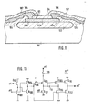
- a thick field oxide 102 is selectively formed on a semiconductor substrate 101.
- a polycrystalline silicon 60 is formed on the field oxide 102.
- the polycrystalline silicon 60 has first and second portions 60a and 60c which are highly doped with an impurity and a third portion 60b in which the impurity concentration is not substantial.
- Aluminum wirings 105 and 106 are formed on silicon-dioxide layer 104 and connected to the first and second portions 60a and 60c of the polycrystalline silicon 60.
- the aluminum wirings 105 and 106 are covered by a silicon-dioxide layer 107.
- the state of the polycrystalline silicon thus obtained corresponds to a high resistance state in which the transistor 100 is conducting.
- the impurity doped in the portions 60a and 60c of the polycrystalline silicon is diffused into the portion 60b by annealing the polycrystalline silicon 60.
- annealing is preferably conducted by heating the polycrystalline silicon 60 by a known laser annealing technique.
- a third embodiment of the present invention will be described. Corresponding portions to those in Figs. 1 and 2 are designated by similar reference numerals.
- This embodiment is obtained by providing a programmable type delay circuit PD" to the memory circuit shown in Fig. 1.
- An input terminal of the delay circuit PD'' is connected to the output terminal of the dealy circuit 1, and an output terminal of the circuit PD" is connected together with the output terminal ($ 4 ) of the delay circuit in a wired-OR connection 70.
- the delay circuit PD" has two programmed states. One state is an active state in which the circuit PD" generates an output signal ⁇ 1 ' in response to the clock signal ⁇ 1 . The other state is an inactive state in which the circuit PD'' never produces the output ⁇ 1 ' irrespective of the clock signal ⁇ 1 .
- the output ⁇ 1 ' of the circuit PD" is connected with the output ⁇ 4 of the delay circuit 4 at the junction 70 in in a wired-OR manner, and hence when the circuit PD" is programmed in the active state, the output ⁇ 4 ' from the junction 70 is the same as the signal ⁇ 1 '. On the other hand, when the circuit PD" is programmed in the inactive state, then the output ⁇ 4 ' becomes the same as the signal ⁇ 4 from the delay circuit.
- Transistors Q 102 to Q 105 form a buffer stage for receiving the signal 1.
- Transistors Q 106 to Q 112 form a boot-strap type delay circuit.
- the signal is applied to a drain of the transistor Q 108 via a fusible link 120.
- the circuit PD" When the fusible link 120 remains uncut, the circuit PD" generates the output signal ⁇ 1 .
- the fusible link is cut, a gate of the transistor Q 109 cannot be raised in potential, and hence the circuit PD" does not produce the signal ⁇ 1 '.
Applications Claiming Priority (2)
| Application Number | Priority Date | Filing Date | Title |
|---|---|---|---|
| JP58078983A JPS59203299A (ja) | 1983-05-06 | 1983-05-06 | 冗長ビット付メモリ |
| JP78983/83 | 1983-05-06 |
Publications (3)
| Publication Number | Publication Date |
|---|---|
| EP0124900A2 true EP0124900A2 (fr) | 1984-11-14 |
| EP0124900A3 EP0124900A3 (en) | 1987-08-26 |
| EP0124900B1 EP0124900B1 (fr) | 1990-11-14 |
Family
ID=13677120
Family Applications (1)
| Application Number | Title | Priority Date | Filing Date |
|---|---|---|---|
| EP84105145A Expired - Lifetime EP0124900B1 (fr) | 1983-05-06 | 1984-05-07 | Circuit de mémoire, de type à redondance, ayant un générateur d'horloge amélioré |
Country Status (4)
| Country | Link |
|---|---|
| US (1) | US4723227A (fr) |
| EP (1) | EP0124900B1 (fr) |
| JP (1) | JPS59203299A (fr) |
| DE (1) | DE3483593D1 (fr) |
Cited By (4)
| Publication number | Priority date | Publication date | Assignee | Title |
|---|---|---|---|---|
| GB2165378A (en) * | 1984-09-26 | 1986-04-09 | Hitachi Ltd | A semiconductor storage device |
| EP0414477A2 (fr) * | 1989-08-25 | 1991-02-27 | Fujitsu Limited | Dispositif de mémoire à semiconducteur ayant des cellules de mémoire redondantes |
| GB2256070A (en) * | 1991-05-24 | 1992-11-25 | Samsung Electronics Co Ltd | Semiconductor memory device with redundancy |
| WO1997043713A1 (fr) * | 1996-05-10 | 1997-11-20 | Memory Corporation Plc | Circuit de temporisation pour memoire de remplacement |
Families Citing this family (23)
| Publication number | Priority date | Publication date | Assignee | Title |
|---|---|---|---|---|
| JPS62222500A (ja) * | 1986-03-20 | 1987-09-30 | Fujitsu Ltd | 半導体記憶装置 |
| JP2580128B2 (ja) * | 1986-07-18 | 1997-02-12 | 日立超エル・エス・アイエンジニアリング株式会社 | 半導体記憶装置 |
| JP2577724B2 (ja) * | 1986-07-31 | 1997-02-05 | 三菱電機株式会社 | 半導体記憶装置 |
| EP0257120B1 (fr) * | 1986-08-22 | 1992-06-10 | International Business Machines Corporation | Procédé et circuit de décodage pour une mémoire redondante à semi-conducteurs CMOS |
| JPS63244494A (ja) * | 1987-03-31 | 1988-10-11 | Toshiba Corp | 半導体記憶装置 |
| US5022006A (en) * | 1988-04-01 | 1991-06-04 | International Business Machines Corporation | Semiconductor memory having bit lines with isolation circuits connected between redundant and normal memory cells |
| JPH02177087A (ja) * | 1988-12-27 | 1990-07-10 | Nec Corp | リダンダンシーデコーダ |
| JPH03252998A (ja) * | 1990-02-28 | 1991-11-12 | Sharp Corp | 半導体記憶装置 |
| US5177744A (en) * | 1990-09-04 | 1993-01-05 | International Business Machines Corporation | Method and apparatus for error recovery in arrays |
| JP2888034B2 (ja) * | 1991-06-27 | 1999-05-10 | 日本電気株式会社 | 半導体メモリ装置 |
| EP0636258B1 (fr) * | 1992-04-16 | 1996-03-27 | Siemens Aktiengesellschaft | Memoire a semi-conducteurs integre a redondance |
| US5557618A (en) * | 1993-01-19 | 1996-09-17 | Tektronix, Inc. | Signal sampling circuit with redundancy |
| US5568433A (en) * | 1995-06-19 | 1996-10-22 | International Business Machines Corporation | Memory array having redundant word line |
| KR100196515B1 (ko) * | 1995-06-30 | 1999-06-15 | 김영환 | 반도체 메모리 장치의 리던던시 회로 |
| US5708613A (en) * | 1996-07-22 | 1998-01-13 | International Business Machines Corporation | High performance redundancy in an integrated memory system |
| US5968180A (en) * | 1997-09-30 | 1999-10-19 | Intel Corporation | Data capture circuit for asynchronous data transfer |
| US6317370B2 (en) | 1998-01-12 | 2001-11-13 | Micron Technology, Inc. | Timing fuse option for row repair |
| KR100340113B1 (ko) * | 1998-06-29 | 2002-09-26 | 주식회사 하이닉스반도체 | 반도체메모리장치 |
| US6134176A (en) * | 1998-11-24 | 2000-10-17 | Proebsting; Robert J. | Disabling a defective element in an integrated circuit device having redundant elements |
| JP3398686B2 (ja) * | 1999-06-14 | 2003-04-21 | エヌイーシーマイクロシステム株式会社 | 半導体記憶装置 |
| US6970045B1 (en) | 2003-06-25 | 2005-11-29 | Nel Frequency Controls, Inc. | Redundant clock module |
| US20090161470A1 (en) * | 2007-12-20 | 2009-06-25 | Micron Technology, Inc. | Circuit for dynamic readout of fused data in image sensors |
| JP6685579B1 (ja) * | 2019-10-21 | 2020-04-22 | 中島 秀夫 | 無電動小旋回身体移動補助機能と電動小旋回身体移動補助機能とを有し自分で自分の体を小旋回移動する天秤介護方法。 |
Family Cites Families (2)
| Publication number | Priority date | Publication date | Assignee | Title |
|---|---|---|---|---|
| JPS5782297A (en) * | 1980-11-11 | 1982-05-22 | Nippon Telegr & Teleph Corp <Ntt> | Semiconductor storage device |
| US4576455A (en) * | 1984-02-10 | 1986-03-18 | Panavision, Inc. | Dual motor reversible drive film magazine |
-
1983
- 1983-05-06 JP JP58078983A patent/JPS59203299A/ja active Granted
-
1984
- 1984-05-04 US US06/607,050 patent/US4723227A/en not_active Expired - Fee Related
- 1984-05-07 DE DE8484105145T patent/DE3483593D1/de not_active Expired - Fee Related
- 1984-05-07 EP EP84105145A patent/EP0124900B1/fr not_active Expired - Lifetime
Non-Patent Citations (2)
| Title |
|---|
| IEEE ELECTRO, vol. 7, no. 26/3, May 1982, pages 1-6, New York, US; J.P. ALTNETHER et al.: "Testing redundant memories" * |
| IEEE JOURNAL OF SOLID-STATE CIRCUITS, vol. Sc-17, no. 4, August 1982, pages 726-731, New York, US; T. MANO et al.: "A redundancy circuit for a fault-tolerant 256K MOS RAM" * |
Cited By (8)
| Publication number | Priority date | Publication date | Assignee | Title |
|---|---|---|---|---|
| GB2165378A (en) * | 1984-09-26 | 1986-04-09 | Hitachi Ltd | A semiconductor storage device |
| US5047983A (en) * | 1984-09-26 | 1991-09-10 | Hitachi, Ltd. | Semiconductor storage device with redundancy arrangement |
| EP0414477A2 (fr) * | 1989-08-25 | 1991-02-27 | Fujitsu Limited | Dispositif de mémoire à semiconducteur ayant des cellules de mémoire redondantes |
| EP0414477A3 (en) * | 1989-08-25 | 1992-08-05 | Fujitsu Limited | Semiconductor memory device having redundant memory cells |
| US5197030A (en) * | 1989-08-25 | 1993-03-23 | Fujitsu Limited | Semiconductor memory device having redundant memory cells |
| GB2256070A (en) * | 1991-05-24 | 1992-11-25 | Samsung Electronics Co Ltd | Semiconductor memory device with redundancy |
| FR2676844A1 (fr) * | 1991-05-24 | 1992-11-27 | Samsung Electronics Co Ltd | Dispositif de memoire a semiconducteurs avec redondance. |
| WO1997043713A1 (fr) * | 1996-05-10 | 1997-11-20 | Memory Corporation Plc | Circuit de temporisation pour memoire de remplacement |
Also Published As
| Publication number | Publication date |
|---|---|
| JPH0250559B2 (fr) | 1990-11-02 |
| US4723227A (en) | 1988-02-02 |
| JPS59203299A (ja) | 1984-11-17 |
| EP0124900A3 (en) | 1987-08-26 |
| DE3483593D1 (de) | 1990-12-20 |
| EP0124900B1 (fr) | 1990-11-14 |
Similar Documents
| Publication | Publication Date | Title |
|---|---|---|
| US4723227A (en) | Redundant type memory circuit with an improved clock generator | |
| US5079744A (en) | Test apparatus for static-type semiconductor memory devices | |
| CN101040343B (zh) | 用于静态随机存取存储器的字线驱动器电路及其方法 | |
| US5200922A (en) | Redundancy circuit for high speed EPROM and flash memory devices | |
| US4365319A (en) | Semiconductor memory device | |
| EP0293339B1 (fr) | Dispositif de mémoire permanente supportant un grand nombre de cycles de programmation | |
| US6256239B1 (en) | Redundant decision circuit for semiconductor memory device | |
| JPH07226100A (ja) | 半導体メモリ装置 | |
| US5748527A (en) | Nonvolatile memory having transistor redundancy | |
| JP2888034B2 (ja) | 半導体メモリ装置 | |
| US5485424A (en) | Semiconductor memory and redundant-address writing method | |
| US6005790A (en) | Floating gate content addressable memory | |
| JPH04232693A (ja) | スタティック型半導体記憶装置 | |
| US4587639A (en) | Static semiconductor memory device incorporating redundancy memory cells | |
| JPS63220500A (ja) | 半導体記憶装置の冗長回路 | |
| US4586170A (en) | Semiconductor memory redundant element identification circuit | |
| US4987560A (en) | Semiconductor memory device | |
| US4571707A (en) | Memory circuit with improved redundant structure | |
| US5453954A (en) | Semiconductor integrated circuit device with built-in regulating system for determining margins of main circuits | |
| US6868021B2 (en) | Rapidly testable semiconductor memory device | |
| US5818778A (en) | Redundancy circuit for programmable integrated circuits | |
| EP0352730B1 (fr) | Dispositif de mémoire semi-conducteur muni d'un système de détection des positions utilisant une structure redondante | |
| US5058070A (en) | High speed memory with row redundancy | |
| JPH07244998A (ja) | 半導体メモリ装置 | |
| US5359563A (en) | Memory system with adaptable redundancy |
Legal Events
| Date | Code | Title | Description |
|---|---|---|---|
| PUAI | Public reference made under article 153(3) epc to a published international application that has entered the european phase |
Free format text: ORIGINAL CODE: 0009012 |
|
| 17P | Request for examination filed |
Effective date: 19840718 |
|
| AK | Designated contracting states |
Designated state(s): DE FR GB |
|
| PUAL | Search report despatched |
Free format text: ORIGINAL CODE: 0009013 |
|
| AK | Designated contracting states |
Kind code of ref document: A3 Designated state(s): DE FR GB |
|
| 17Q | First examination report despatched |
Effective date: 19900109 |
|
| GRAA | (expected) grant |
Free format text: ORIGINAL CODE: 0009210 |
|
| AK | Designated contracting states |
Kind code of ref document: B1 Designated state(s): DE FR GB |
|
| REF | Corresponds to: |
Ref document number: 3483593 Country of ref document: DE Date of ref document: 19901220 |
|
| ET | Fr: translation filed | ||
| PLBE | No opposition filed within time limit |
Free format text: ORIGINAL CODE: 0009261 |
|
| STAA | Information on the status of an ep patent application or granted ep patent |
Free format text: STATUS: NO OPPOSITION FILED WITHIN TIME LIMIT |
|
| 26N | No opposition filed | ||
| PGFP | Annual fee paid to national office [announced via postgrant information from national office to epo] |
Ref country code: GB Payment date: 19950427 Year of fee payment: 12 |
|
| PGFP | Annual fee paid to national office [announced via postgrant information from national office to epo] |
Ref country code: FR Payment date: 19950517 Year of fee payment: 12 |
|
| PGFP | Annual fee paid to national office [announced via postgrant information from national office to epo] |
Ref country code: DE Payment date: 19950721 Year of fee payment: 12 |
|
| PG25 | Lapsed in a contracting state [announced via postgrant information from national office to epo] |
Ref country code: GB Effective date: 19960507 |
|
| GBPC | Gb: european patent ceased through non-payment of renewal fee |
Effective date: 19960507 |
|
| PG25 | Lapsed in a contracting state [announced via postgrant information from national office to epo] |
Ref country code: FR Effective date: 19970131 |
|
| PG25 | Lapsed in a contracting state [announced via postgrant information from national office to epo] |
Ref country code: DE Effective date: 19970201 |
|
| REG | Reference to a national code |
Ref country code: FR Ref legal event code: ST |