EP0115892B1 - X-ray examination apparatus having a double focusing crystal - Google Patents
X-ray examination apparatus having a double focusing crystal Download PDFInfo
- Publication number
- EP0115892B1 EP0115892B1 EP19840200132 EP84200132A EP0115892B1 EP 0115892 B1 EP0115892 B1 EP 0115892B1 EP 19840200132 EP19840200132 EP 19840200132 EP 84200132 A EP84200132 A EP 84200132A EP 0115892 B1 EP0115892 B1 EP 0115892B1
- Authority
- EP
- European Patent Office
- Prior art keywords
- crystal
- double focusing
- jig
- single crystal
- ray
- Prior art date
- Legal status (The legal status is an assumption and is not a legal conclusion. Google has not performed a legal analysis and makes no representation as to the accuracy of the status listed.)
- Expired
Links
- 239000013078 crystal Substances 0.000 title claims description 116
- 230000005855 radiation Effects 0.000 claims description 25
- 238000002441 X-ray diffraction Methods 0.000 claims description 10
- 238000004458 analytical method Methods 0.000 claims description 7
- 239000003292 glue Substances 0.000 claims description 7
- 229910052751 metal Inorganic materials 0.000 claims description 7
- 239000002184 metal Substances 0.000 claims description 7
- 239000000463 material Substances 0.000 claims description 6
- 229910052710 silicon Inorganic materials 0.000 claims description 5
- 239000010703 silicon Substances 0.000 claims description 5
- 238000005304 joining Methods 0.000 claims description 4
- 150000001875 compounds Chemical class 0.000 claims description 2
- 229910052732 germanium Inorganic materials 0.000 claims description 2
- GNPVGFCGXDBREM-UHFFFAOYSA-N germanium atom Chemical compound [Ge] GNPVGFCGXDBREM-UHFFFAOYSA-N 0.000 claims description 2
- 238000000034 method Methods 0.000 description 6
- 238000005259 measurement Methods 0.000 description 5
- XUIMIQQOPSSXEZ-UHFFFAOYSA-N Silicon Chemical compound [Si] XUIMIQQOPSSXEZ-UHFFFAOYSA-N 0.000 description 4
- 230000005540 biological transmission Effects 0.000 description 3
- 239000011888 foil Substances 0.000 description 3
- 238000005476 soldering Methods 0.000 description 3
- OAICVXFJPJFONN-UHFFFAOYSA-N Phosphorus Chemical compound [P] OAICVXFJPJFONN-UHFFFAOYSA-N 0.000 description 2
- HCHKCACWOHOZIP-UHFFFAOYSA-N Zinc Chemical compound [Zn] HCHKCACWOHOZIP-UHFFFAOYSA-N 0.000 description 2
- 230000002411 adverse Effects 0.000 description 2
- 239000000843 powder Substances 0.000 description 2
- 230000035882 stress Effects 0.000 description 2
- 239000011701 zinc Substances 0.000 description 2
- 229910052725 zinc Inorganic materials 0.000 description 2
- 229910000906 Bronze Inorganic materials 0.000 description 1
- RYGMFSIKBFXOCR-UHFFFAOYSA-N Copper Chemical compound [Cu] RYGMFSIKBFXOCR-UHFFFAOYSA-N 0.000 description 1
- 229910002483 Cu Ka Inorganic materials 0.000 description 1
- RTAQQCXQSZGOHL-UHFFFAOYSA-N Titanium Chemical compound [Ti] RTAQQCXQSZGOHL-UHFFFAOYSA-N 0.000 description 1
- 230000032683 aging Effects 0.000 description 1
- 238000005452 bending Methods 0.000 description 1
- 239000010974 bronze Substances 0.000 description 1
- 238000001816 cooling Methods 0.000 description 1
- 229910052802 copper Inorganic materials 0.000 description 1
- 239000010949 copper Substances 0.000 description 1
- KUNSUQLRTQLHQQ-UHFFFAOYSA-N copper tin Chemical compound [Cu].[Sn] KUNSUQLRTQLHQQ-UHFFFAOYSA-N 0.000 description 1
- 230000003247 decreasing effect Effects 0.000 description 1
- 238000000151 deposition Methods 0.000 description 1
- 230000008021 deposition Effects 0.000 description 1
- 238000009792 diffusion process Methods 0.000 description 1
- 230000002349 favourable effect Effects 0.000 description 1
- 239000007788 liquid Substances 0.000 description 1
- 238000004519 manufacturing process Methods 0.000 description 1
- 229910021421 monocrystalline silicon Inorganic materials 0.000 description 1
- 229910052698 phosphorus Inorganic materials 0.000 description 1
- 239000011574 phosphorus Substances 0.000 description 1
- 239000011148 porous material Substances 0.000 description 1
- 239000007787 solid Substances 0.000 description 1
- 238000009987 spinning Methods 0.000 description 1
- 238000004544 sputter deposition Methods 0.000 description 1
- 239000007858 starting material Substances 0.000 description 1
- 239000010936 titanium Substances 0.000 description 1
- 229910052719 titanium Inorganic materials 0.000 description 1
- 238000011282 treatment Methods 0.000 description 1
Images

Classifications
-
- G—PHYSICS
- G01—MEASURING; TESTING
- G01N—INVESTIGATING OR ANALYSING MATERIALS BY DETERMINING THEIR CHEMICAL OR PHYSICAL PROPERTIES
- G01N23/00—Investigating or analysing materials by the use of wave or particle radiation, e.g. X-rays or neutrons, not covered by groups G01N3/00 – G01N17/00, G01N21/00 or G01N22/00
- G01N23/20—Investigating or analysing materials by the use of wave or particle radiation, e.g. X-rays or neutrons, not covered by groups G01N3/00 – G01N17/00, G01N21/00 or G01N22/00 by using diffraction of the radiation by the materials, e.g. for investigating crystal structure; by using scattering of the radiation by the materials, e.g. for investigating non-crystalline materials; by using reflection of the radiation by the materials
- G01N23/207—Diffractometry using detectors, e.g. using a probe in a central position and one or more displaceable detectors in circumferential positions
Definitions
- the invention relates to a double focusing X-ray analysis crystal for monochromatization and focusing of X-ray radiation according to the preamble of claim 1.
- Such an X-ray analysis crystal is known from British Patent Specification 1,089,714.
- An analysis crystal described therein is curved in two directions with different radii of curvature in order to obtain a double focusing.
- the process of bending a crystal into such a form is fairly difficult and in this process the crystal is liable to break or the curvature nevertheless deviates from the envisaged optimum curvature due to a later deformation.
- the crystal is constantly in a forced condition, as a result of which deformations are liable to occur during operation, for example, due to temperature variations or ageing phenomena. Further, it is of importance that the back surface of the crystal is not disturbed because irregularities therein may adversely affect the operation of the crystal as a monochromator.
- the invention has for its object to obviate these disadvantages and therefore an X-ray analysis crystal of the kind mentioned in the opening paragraph is provided as defined by Claim 1.
- the crystal is arranged by means of a glue compound in a jig comprising a material porous to the glue. More particularly, the jig has a radius of curvature 2R and the active crystal surface has a radius of curvature R. It is possible to provide a planar crystal in the jig and then to grind the active surface to the desired curvature, whilst it is also possible to first provide the crystal with a curvature, which, after the crystal has been mounted in the jig, together with the curvature of the jig leads to the desired curvature.
- the crystal can be coated on the non-active flat side with a layer of metal, which may be applied, for example, by vapour deposition, sputtering or spinning in a layer having a very homogeneous thickness. With this layer as a joining intermediate layer, the crystal may then be secured again in the jig, for example, by soldering or diffusion, which jig then need not be porous.
- the metal layer may be applied in the form of a metal foil; this is particularly favourable with the use of a crystal material which in itself is brittle or of low strength. With a metal foil of, for example, phosphor bronze, a very flexible element of high strengh can nevertheless be obtained.
- the back side of the crystal may also be formed so that the crystal ultimately has an at least substantially uniform thickness. The surface of the back side of the crystal should be very flat because irregularities therein can adversely affect the operation of the crystal.
- the crystal consists of a single crystal of silicon or germanium poor in dislocations, which, when mounted in the jig, is only elastically deformed.
- the single crystal is then, for example, a slice cut along a crystal surface. After the spherical deformation, a centre of curvature of the said crystal surface lies on a Rowland sphere on which with a close approximation will be located also the centres of curvatures of some further crystal surfaces with decreasing crystal surface distance.
- the crystal acts as a monochromator in an X-ray analysis apparatus, whereby now for a complete analysis a fixed position of the specimen and two positions of the analysis crystal and a single scanning along the arc of a circle of the detector will be sufficient. In this case, the resolution and the signal-to-noise ratio can also be materially improved.
- the crystal according to the invention can further be used successfully in, for example, a diffractometer in which, for example, use is made of a converging Cu-Ka 1 radiation boom, and in apparatus for stress examination or texture measurements.
- Figure 1 shows a silicon single crystal 1 of which an active surface 3 forms part of a sphere 5 on which centres of curvature 7 of distinct crystal surfaces are located.
- the centres of curvature for crystal surfaces (124), (113), (022) and (111) for a crystal formed from a slice of material parallel to the (124) crystal surfaces thereof are indicated as such in this configuration, the exact centre of curvature for the crystal surfaces (124) is located on the surface of the sphere and for other groups of crystal surfaces approximate centres of curvature are located on the surface of the sphere.
- the sphere 5, also designated as Rowland sphere, is determined by the position and the radius of curvature of the crystal and the (124) centre of curvature.
- centres of curvature mentioned below are located at least substantially on the surface of the sphere in such a manner that the centres of curvature for the crystal surface (113) and (022) are located with the centre of curvature for the crystal surface (124) on the circle circumference of .
- the circle 9 passing through the centre 11 of the sphere 5 while the centre of curvature for the crystal surface (111) is located with the centre of curvature (124) on a circle circumference of a circle 13 orientated at right angles thereto and passing through the centre 11.
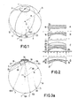
- Such a crystal is formed by means of a method to be described in Figure 2, in which the starting material is a slice 15 of monocrystalline silicon poor in dislocations shown in Figure 2a.
- Parallel surfaces 17 and 19 of the crystal extend (in this case) parallel to the (124) crystal surfaces, while in the crystal the crystal surfaces (022) and (113) are indicated diagrammatically.
- the crystal is then excavated, for example, by grinding, until a spherical surface 21 having a radius of curvature 2R and shown in Figure 2B is obtained.
- a jig 23 shown in Figure 2C and formed in this case from a porous material is correspondingly excavated on one side until a spherical surface 25 is obtained which, for example, also has a radius of curvature 2R.
- a glue foil 27 With the interposition of a glue foil 27, the ground crystal 15 is then pressed into the jig.
- a diaphragm 29 which is pressed by means of gas or liquid pressure against the crystal surface 21 in such a manner that it is loaded at least substantially homogeneously. In this process, it is recommendable for obtaining a good adherence to heat the assembly to, for example, 180°C and to eliminate the pressure only after cooling.
- the temperature can be adapted to the glue and the excess quantity of glue is absorbed by the porous jig.
- a combination 30 of crystal and jig thus formed and shown in Figure 2D constitutes a robust element to be readily manipulated for X-ray analysis apparatus suiting the purpose.
- the active surface 21 of the crystal has by a combination of treatments a radius of curvature R which corresponds to that of the sphere 5 in Figure 1.
- the combination 30 may also be used. However, it is required to mount the crystal with adherence at least along its whole circumference and preferably throughout the whole non-active surface 19. As a result, the possibility of later deformation is strongly reduced. As already indicated, the crystal may alternatively be mounted in the jig by soldering with the interposition of a metal layer, whereby irregularities in the layer thickness of the soldering material have to be avoided.
- Figure 3 shows the radiation path in an X-ray apparatus for analysing a specimen 31 by means of a silicon single crystal 15 thus formed.
- Figure 3a shows the circle 9 of Figure 1 with the centre of curvature (022), (124) and (113), while Figure 3b shows the circle 13 of Figure 1 with the centres of curvatures (124) and (111).
- Figure 3a shows the difference between Figure 3a and Figure 3b is a rotation of the crystal 15 through 90° about an axis passing through the centre of curvature (124).
- a conical beam trapped by the crystal is focused by the crystal in a line on the circle circumference.
- the cone is determined by the solid angle viewed from the point of intersection of a Bragg condition applying to the relevant crystal surface and the circumference of the crystal.
- a cone 33 is trapped by the crystal, of which radiation of the wavelength applying to the relevant crystal surfaces, in this case the (113) surfaces, is focused as a conical beam 34 in a line 35 located on the circle 9.
- the. intensity and hence the zinc content in the specimen can be measured.
- radiation of a wavelength characteristic of titanium from a cone 37 is concentrated by (022) crystal surfaces in the crystal via a conical beam 38 to a line 39 on the circle.
- the focus lines for, for example, Ca(20) to Co(27) of Ka1 radiation diffracted at the (022) crystal surfaces are located on either side of the point 39, which also applies to the focus lines for, for example, Sn(51) to Tm(69) of La1 radiation also diffracted at the (22) crystal surfaces of the crystal.
- a powder diffractometer shows a radiation source 51, for example, the target of an anode in an X-ray tube, a spherically curved single crystal 53, a specimen 55 in transmission position and a specimen 57 in reflection position.
- the source 51 and the crystal 53 are located on a Rowland sphere 60, on which a focus 62 of an X-ray beam 64 focused by the crystal is also located.
- the X-ray radiation is, for example, copper Ka1 radiation.
- radiation diffracted at distinct crystal surfaces of the specimen 55 is focused by transmission in distinct focus lines 61 and 63 of the circumference of a focus sphere 66.
- the specimen For reflection, radiation diffracted at distinct crystal surfaces of the specimen is focussed in focus lines 65 and 67 on the circumference of a focus sphere 68. With detectors 69 moving along these spheres or with position-sensitive detectors mounted along these spheres, the local intensity may now again be measured simultaneously for transmission and reflection.
- the specimen can be displaced within the beam path through a distance equal to twice the diameter of the sphere 66 in a correct angular relationship.
- An X-ray analysis apparatus designed for measuring macro-stresses in, for example, work pieces provided with a crystal according to the invention, comprises, as shown in Figure 5, an X-ray source 70, a spherical analysis crystal 72, a specimen 74 with, for example crystal surfaces 76 and a, for example, position-sensitive detector 78 by which the radiation intensity can be measured as a function of the deflection angle.
- the source 70, the crystal 72 and the beam focus 80 of an X-ray beam 82 are located on a Rowland sphere 84.
- the beam focus 80, an irradiated specimen surface 86 and a focus line 88 of a diffracted beam 92 are located on a Rowland sphere 96.
- the focus line 88 applying to, for example, a specimen or a direction in a specimen in which no macro-stresses are present, shifts to a focus line 90 for a specimen or a direction in a specimen in which macro-stresses are present.
- the arc distance between the focus line 88 and the focus line 90 is a measure for the value of the macro-stresses in the specimen measured in a given crystal direction. This value can be measured by exchange of specimens, whereby, for example, in order to determine the position of the focus line 88, first a stress-free specimen is measured and then specimens with unknown macro-stresses are measured. Further, a specimen can be rotated before the measurement, whereby either by an additional measurement or by an iteration process the position of a focus line of a stress-free measurment can be determined with the measurement results.
Landscapes
- Chemical & Material Sciences (AREA)
- Crystallography & Structural Chemistry (AREA)
- Physics & Mathematics (AREA)
- Health & Medical Sciences (AREA)
- Life Sciences & Earth Sciences (AREA)
- Analytical Chemistry (AREA)
- Biochemistry (AREA)
- General Health & Medical Sciences (AREA)
- General Physics & Mathematics (AREA)
- Immunology (AREA)
- Pathology (AREA)
- Analysing Materials By The Use Of Radiation (AREA)
Applications Claiming Priority (2)
| Application Number | Priority Date | Filing Date | Title |
|---|---|---|---|
| NL8300421A NL8300421A (nl) | 1983-02-04 | 1983-02-04 | Roentgen onderzoek apparaat met dubbel focusserend kristal. |
| NL8300421 | 1983-02-04 |
Publications (2)
| Publication Number | Publication Date |
|---|---|
| EP0115892A1 EP0115892A1 (en) | 1984-08-15 |
| EP0115892B1 true EP0115892B1 (en) | 1987-08-19 |
Family
ID=19841350
Family Applications (1)
| Application Number | Title | Priority Date | Filing Date |
|---|---|---|---|
| EP19840200132 Expired EP0115892B1 (en) | 1983-02-04 | 1984-02-01 | X-ray examination apparatus having a double focusing crystal |
Country Status (5)
| Country | Link |
|---|---|
| EP (1) | EP0115892B1 (enExample) |
| JP (1) | JPS59153152A (enExample) |
| CA (1) | CA1222075A (enExample) |
| DE (1) | DE3465519D1 (enExample) |
| NL (1) | NL8300421A (enExample) |
Cited By (1)
| Publication number | Priority date | Publication date | Assignee | Title |
|---|---|---|---|---|
| US7248670B2 (en) | 2002-06-19 | 2007-07-24 | Xenocs | Optical unit and associated method |
Families Citing this family (6)
| Publication number | Priority date | Publication date | Assignee | Title |
|---|---|---|---|---|
| NL8501181A (nl) * | 1985-04-24 | 1986-11-17 | Philips Nv | Kristal voor een roentgenanalyse apparaat. |
| JPS62141730U (enExample) * | 1986-02-28 | 1987-09-07 | ||
| WO1996034274A2 (en) * | 1995-04-26 | 1996-10-31 | Philips Electronics N.V. | Method of manufacturing an x-ray optical element for an x-ray analysis apparatus |
| FR2841371B1 (fr) * | 2002-06-19 | 2004-10-22 | Xenocs | Ensemble optique et procede associe |
| CN107024493A (zh) * | 2017-03-20 | 2017-08-08 | 中国工程物理研究院电子工程研究所 | 一种碳化硅单晶晶片基平面弯曲的测试方法 |
| CN114649106B (zh) * | 2022-03-17 | 2024-08-27 | 重庆大学 | 一种球面高能透射晶体成像器及制造方法 |
Family Cites Families (6)
| Publication number | Priority date | Publication date | Assignee | Title |
|---|---|---|---|---|
| NL6410514A (enExample) * | 1964-09-10 | 1966-03-11 | ||
| JPS454549Y1 (enExample) * | 1968-10-11 | 1970-03-02 | ||
| JPS5023994A (enExample) * | 1973-07-02 | 1975-03-14 | ||
| US3927319A (en) * | 1974-06-28 | 1975-12-16 | Univ Southern California | Crystal for X-ray crystal spectrometer |
| US4078175A (en) * | 1976-09-20 | 1978-03-07 | Nasa | Apparatus for use in examining the lattice of a semiconductor wafer by X-ray diffraction |
| DD149420A1 (de) * | 1980-03-03 | 1981-07-08 | Reinhard Arnhold | Roentgendiffraktometer |
-
1983
- 1983-02-04 NL NL8300421A patent/NL8300421A/nl not_active Application Discontinuation
-
1984
- 1984-02-01 EP EP19840200132 patent/EP0115892B1/en not_active Expired
- 1984-02-01 DE DE8484200132T patent/DE3465519D1/de not_active Expired
- 1984-02-01 CA CA000446511A patent/CA1222075A/en not_active Expired
- 1984-02-03 JP JP59017218A patent/JPS59153152A/ja active Granted
Cited By (1)
| Publication number | Priority date | Publication date | Assignee | Title |
|---|---|---|---|---|
| US7248670B2 (en) | 2002-06-19 | 2007-07-24 | Xenocs | Optical unit and associated method |
Also Published As
| Publication number | Publication date |
|---|---|
| JPH0557536B2 (enExample) | 1993-08-24 |
| EP0115892A1 (en) | 1984-08-15 |
| NL8300421A (nl) | 1984-09-03 |
| CA1222075A (en) | 1987-05-19 |
| JPS59153152A (ja) | 1984-09-01 |
| DE3465519D1 (en) | 1987-09-24 |
Similar Documents
| Publication | Publication Date | Title |
|---|---|---|
| US4599741A (en) | System for local X-ray excitation by monochromatic X-rays | |
| EP0117293B1 (en) | Stress measurement by x-ray diffractometry | |
| US7076024B2 (en) | X-ray apparatus with dual monochromators | |
| US6882739B2 (en) | Method and apparatus for rapid grain size analysis of polycrystalline materials | |
| US5509043A (en) | Asymmetrical 4-crystal monochromator | |
| EP2042860B1 (en) | X-ray diffraction apparatus and x-ray diffraction method | |
| EP0110469B1 (en) | X-ray analysis apparatus comprising a four-crystal monochromator | |
| US4649557A (en) | X-ray analysis apparatus including a monochromator crystal having crystal lattice surfaces | |
| US5414747A (en) | Method and apparatus for in-process analysis of polycrystalline films and coatings by x-ray diffraction | |
| JP2001021507A (ja) | Xafs測定装置 | |
| EP0115892B1 (en) | X-ray examination apparatus having a double focusing crystal | |
| US4078175A (en) | Apparatus for use in examining the lattice of a semiconductor wafer by X-ray diffraction | |
| US2805342A (en) | Diffractometer | |
| KR20040089115A (ko) | 회절 분석기 및 회절 분석 방법 | |
| JPH1114561A (ja) | X線測定装置およびその方法 | |
| US5914997A (en) | X-ray spectrometer with an analyzer crystal having a partly variable and a partly constant radius of curvature | |
| JP2000155102A (ja) | X線測定装置およびその方法 | |
| JP2006194888A (ja) | X線拡散を使用した原位置温度測定装置 | |
| JPS61186839A (ja) | ラウエカメラ | |
| US3148275A (en) | Specimen holder for X-ray powder analysis | |
| US11221304B2 (en) | Method for measuring stress | |
| US3200248A (en) | Apparatus for use as a goniometer and diffractometer | |
| JPH04164239A (ja) | 粉末x線回折計 | |
| Winegar | Measurement of crystallographic texture at chalk river nuclear laboratories | |
| FR2587805A1 (fr) | Procede et dispositif de determination de la texture cristallographique d'un materiau polycristallin |
Legal Events
| Date | Code | Title | Description |
|---|---|---|---|
| PUAI | Public reference made under article 153(3) epc to a published international application that has entered the european phase |
Free format text: ORIGINAL CODE: 0009012 |
|
| AK | Designated contracting states |
Designated state(s): CH DE FR GB LI NL |
|
| 17P | Request for examination filed |
Effective date: 19841012 |
|
| GRAA | (expected) grant |
Free format text: ORIGINAL CODE: 0009210 |
|
| AK | Designated contracting states |
Kind code of ref document: B1 Designated state(s): CH DE FR GB LI NL |
|
| REF | Corresponds to: |
Ref document number: 3465519 Country of ref document: DE Date of ref document: 19870924 |
|
| ET | Fr: translation filed | ||
| PLBE | No opposition filed within time limit |
Free format text: ORIGINAL CODE: 0009261 |
|
| STAA | Information on the status of an ep patent application or granted ep patent |
Free format text: STATUS: NO OPPOSITION FILED WITHIN TIME LIMIT |
|
| 26N | No opposition filed | ||
| PG25 | Lapsed in a contracting state [announced via postgrant information from national office to epo] |
Ref country code: NL Effective date: 19890901 |
|
| NLV4 | Nl: lapsed or anulled due to non-payment of the annual fee | ||
| REG | Reference to a national code |
Ref country code: CH Ref legal event code: PFA Free format text: PHILIPS ELECTRONICS N.V. |
|
| REG | Reference to a national code |
Ref country code: FR Ref legal event code: CD |
|
| PGFP | Annual fee paid to national office [announced via postgrant information from national office to epo] |
Ref country code: FR Payment date: 19960228 Year of fee payment: 13 |
|
| PGFP | Annual fee paid to national office [announced via postgrant information from national office to epo] |
Ref country code: DE Payment date: 19960424 Year of fee payment: 13 |
|
| PGFP | Annual fee paid to national office [announced via postgrant information from national office to epo] |
Ref country code: CH Payment date: 19960523 Year of fee payment: 13 |
|
| PGFP | Annual fee paid to national office [announced via postgrant information from national office to epo] |
Ref country code: GB Payment date: 19970203 Year of fee payment: 14 |
|
| PG25 | Lapsed in a contracting state [announced via postgrant information from national office to epo] |
Ref country code: LI Free format text: LAPSE BECAUSE OF THE APPLICANT RENOUNCES Effective date: 19970228 Ref country code: CH Free format text: LAPSE BECAUSE OF THE APPLICANT RENOUNCES Effective date: 19970228 |
|
| REG | Reference to a national code |
Ref country code: CH Ref legal event code: PL |
|
| PG25 | Lapsed in a contracting state [announced via postgrant information from national office to epo] |
Ref country code: FR Effective date: 19971030 |
|
| PG25 | Lapsed in a contracting state [announced via postgrant information from national office to epo] |
Ref country code: DE Effective date: 19971101 |
|
| REG | Reference to a national code |
Ref country code: FR Ref legal event code: ST |
|
| PG25 | Lapsed in a contracting state [announced via postgrant information from national office to epo] |
Ref country code: GB Free format text: LAPSE BECAUSE OF NON-PAYMENT OF DUE FEES Effective date: 19980201 |
|
| GBPC | Gb: european patent ceased through non-payment of renewal fee |
Effective date: 19980201 |