EP0103132A2 - Pufferspeichersteuerungsanordnung - Google Patents
Pufferspeichersteuerungsanordnung Download PDFInfo
- Publication number
- EP0103132A2 EP0103132A2 EP83107561A EP83107561A EP0103132A2 EP 0103132 A2 EP0103132 A2 EP 0103132A2 EP 83107561 A EP83107561 A EP 83107561A EP 83107561 A EP83107561 A EP 83107561A EP 0103132 A2 EP0103132 A2 EP 0103132A2
- Authority
- EP
- European Patent Office
- Prior art keywords
- buffer
- address
- buffer storage
- data
- register
- Prior art date
- Legal status (The legal status is an assumption and is not a legal conclusion. Google has not performed a legal analysis and makes no representation as to the accuracy of the status listed.)
- Granted
Links
Images

Classifications
-
- G—PHYSICS
- G06—COMPUTING; CALCULATING OR COUNTING
- G06F—ELECTRIC DIGITAL DATA PROCESSING
- G06F12/00—Accessing, addressing or allocating within memory systems or architectures
- G06F12/02—Addressing or allocation; Relocation
- G06F12/08—Addressing or allocation; Relocation in hierarchically structured memory systems, e.g. virtual memory systems
- G06F12/0802—Addressing of a memory level in which the access to the desired data or data block requires associative addressing means, e.g. caches
- G06F12/0844—Multiple simultaneous or quasi-simultaneous cache accessing
- G06F12/0846—Cache with multiple tag or data arrays being simultaneously accessible
- G06F12/0848—Partitioned cache, e.g. separate instruction and operand caches
Definitions
- the present invention relates to a buffer storage control system in a data processing system having a buffer storage.
- a buffer storage In the data processing system provided with a buffer storage, the latter is realized in a smaller capacity and operated at a higher speed than a main storage, so that a part of data held in the main storage and utilized at a high frequency is stored in the buffer storage to be used at a high speed. Addresses of the data held by the buffer storage are stored in a buffer directory which serves to indicate whether the data of an address to which an access request is issued is present or not in the buffer storage. Further, in a data processing system of virtual address type, there is provided an address translation buffer for holding translation pairs each consisting of a logical address and a corresponding real address.
- the corresponding real address is determined by the address translation buffer, while the buffer directory is searched to determine if the data of the address to which the access request is issued is present in the buffer storage. If the data in concern is found to be present, the buffer storage is accessed to fetch or store data as required.
- Techniques for accessing the address translation buffer, the buffer directory and the buffer storage are disclosed for example in U.S.P. 3,761,881 (issued Sept. 25, 1973), Japanese Laid-open Patent Application No. 10638/1974.
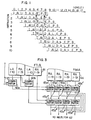
- processing for a single instruction is divided into a plurality of steps with each of the steps in turn being processed through a plurality of stages which can be activated independent of one another, so that a plurality of instructions can be simultaneously processed.
- a reference letter I represents an instruction fetch
- a i represents accesses made to the address translation buffer and the buffer directory by the instruction fetch I
- L i represents an access to the buffer storage made by the instruction fetch I
- D represents a decoding cycle
- A represents accesses made to the address translation buffer and the buffer directory by an operand fetch
- L represents an access to the buffer storage by the operand fetch
- E represents an instruction execution cycle (during which the address translation buffer and the buffer directory are accessed for storing in the case of a store instruction)
- P represents a transfer cycle for the result of the execution
- S represents a store cycle for the buffer storage.
- 3,618,041 (issued November 2, 1971) discloses a memory control system in which the buffer directory and the buffer storage are divisionally and separately provided for the instruction fetch and the operand fetch, respectively, so as to be accessed independent of each other. With such arrangement, the confliction or competition of the accesses for the instruction fetch and the operand fetch can certainly be evaded. However, it is impossible in this known system to evade the competition in access between the store operation and the instruction fetch operation on one hand and between the store operation and the operand fetch operation on the other hand.
- instruction 1 is a store instruction and that instructions 2 to 10 are load instructions.
- the accesses to the address translation buffer and the buffer directory for the store operation are simultaneously issued at the stage E of the instruction 1 in the cycle 6.
- they compete with the accesses to the address translation buffer and the buffer directory made for the operand fetch issued at the stage A of the instruction 3 and the instruction fetch issued at the stage A i of the instruction 6, both stages A and A. belonging to the same cycle 6.
- the access to the buffer storage for realizing the store instruction 1 will compete with the accesses for reading from the buffer storage tried in response to the operand fetch issued at the stage L of the instruction 4 and the instruction fetch making appearance at the stage L i of the instruction 7, both stages coinciding with the same cycle 8.
- Another object of the present invention is to provide a buffer storage control system in which competition for the access to a buffer directory between fetch and store instructions is removed or at least mitigated.
- a further object of the present invention is to provide a buffer storage control system in which competition between the fetch and store instructions for the access to an address translation buffer and a buffer directory is removed or at least mitigated.
- a storage control system which comprises buffer storage means for holding data, first register means in which an address required for realizing a fetch request to the buffer storage is set or placed, second register means in which an address required for a store request is set, and third register means in which data for a store operation are set. Further, the storage control system includes first buffer directory means and second buffer directory means.
- the first buffer directory means is supplied with the address from the first register means and indicates whether or not data designated by said address is held by th buffer storage means.
- the second buffer directory means is supplied with the address from the second register means and indicates whether or not data designated by said address is held by the buffer storage means.
- the buffer storage means fetches the data as requested or stores the data in the third register means. In this way, the fetch request and the store request are distributed to the first buffer directory means and-the second buffer directory means, whereby competition for access can be alleviated.
- first and second address translation buffers for translating logical addresses into real addresses are provided in association with the first and the second register means, respectively.
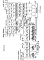
- Fig. 2 shows in a block diagram a general arrangement of a buffer storage control system according to an embodiment of the invention.
- reference numerals 1 to 31 are used to designate bit positions of addresses while numerals greater than 40, inclusive, are used for denoting various components of the system.
- a logical address for fetch operations i.e. instruction fetch or operand fetch is placed in a logical address register for fetch operation (hereinafter also referred to as FLAR in abridgment) 40 from a processor not shown, while a logical address for store operation is placed in logical address register for store operation (hereinafter also referred to as SLAR) 50 from the processor.
- FLAR in abridgment a logical address register for fetch operation
- SLAR logical address register for store operation
- the logical address set in the FLAR 40 is supplied for accessing to a translation look-aside buffer for fetch operation (hereinafter also referred to simply as FTLB) 41 which constitutes an address translation buffer for fetch operation and a buffer address array for fetch operation (hereinafter referred to as FBAA) 44 which constitutes a buffer directory for fetch operation.
- FTLB41 has 512 columns in two rows. For selecting one of these columns, bits 11 to 19 of the address placed in the FLAR 40 is made use of as the column address. Each of the columns holds two addresses translation pairs each consisting of bits 1 to 10 of the logical address LA and bits 1 to 19 of the corresponding real address RA. The address translation pairs which are selected by bits 11 to 19 of the address placed in the FLAR 40 are read out.
- the bits 1 to 10 of the two logical addresses as read out are compared with the bits 1 to 10 of the FLAR 40 which do not constitute the aforementioned column address through comparators 42a and 42b, respectively.
- the outputs of the comparators 42a and 42b are supplied to a selector 43 which then outputs the real address corresponding to the logical address for which coincidence is resulted from the aforementioned comparison. Accordingly, there makes appearance at the output of the selector 43 the real address corresponding to the logical address of the FLAR 40.
- a known address translation process in which an address translation table is made use of is activated. However, since the address translation process constitutes no part directly relevant to the subject of the present invention, any further description will be unnecessary.
- the FBAA 44 comprises 64 columns in four row. For selecting one of these columns, bits 20 to 25 of the address placed in the FLAR 40 are used.
- the FBAA 40 serves to hold bits 1 to 19 of the real address for the data held by a buffer storage (BS) 61 described hereinafter.
- Four real addresses are read out from the column of FBAA 44 selected by the. bits 20 to 25 of the address set in the FLAR 40 and compared with the real address supplied from the selector 43 through comparators 45a, 45b, 45c and 45d, respectively. In case coincidence is found in any one of these comparisons, this means that the data required is present at a row of the buffer storage 61 which row corresponds to the row from which the real address resulting in coincidence in the comparison is read out.
- the bits 20 to 28 of the same address is supplied to a buffer storage address register (hereinafter referred to as BSAR) 60 to thereby permit access to the buffer storage (BS) 61 in parallel with the accesses to the FTLB 41 and FBAA 44.
- the buffer storage or BS 61 is configured in four rows. Data of 8 bytes is read out from each of the rows of BS61 and supplied to a selector 62 which has other inputs supplied with the outputs of the comparators 45a, 45b, 45c and 45d, respectively.
- the selector 62 selects the 8-byte data which corresponds to the row for which coincidence has been detected in the comparisons made by the comparators 45a, .., 45d.
- a logical address for store operation set at a logical address register for store operation (hereinafter referred to as SLAR) 50 is supplied for access to a translation look-aside buffer for store operation (hereinafter referred to as STLB) 51 which constitutes an address translation buffer for store operation and a buffer address array for store operation (hereinafter referred to as SBAA) 54 which constitutes a buffer directory for store operation.
- STLB 51, comparators 52a and 52b, a selector 53, the SBAA 54 and comparators 55a to 55d are arranged in the same configuration as the FTLB 41 for fetch operation, the comparators 42a and 42b, the selector 43, the FBAA 44 and the comparators 45a to 45d to serve for the same functions.
- the contents held by the STLB 51 and the SBAA 54 are same as those held by the FTLB 41 and FBAA 44. It should however be pointed out that while the FTLB 41, the FBAA 44 and the BS 61 are accessed in parallel with one another in the case of the fetch operation, the STLB 51 and the SBAA 54 are accessed in parallel and subsequently the BS 61 is accessed if the required data is present in the latter in the case of the store operation.
- the store data is set in a store data register or SDR 63. When coincidence output is obtained from one of the comparators 55a to 55d, corresponding one of gates 64a to 64d is opened to allow the data of 8 bytes set in the SDR 63 to be stored in the buffer storage or BS 61.
- the buffer storage address register or BSAR 60 is supplied with a signal indicating which of the fetch and the store operations is requested by the processor not shown.
- the address of the address register 40 or 50 corresponding to the request is placed in the BSAR 60 to be supplied to the BS 61 as the column address.
- the store request may be selected with preference over the fetch request, for example, whereby the store address of the SLAR 50 is set in the BSAR 60 to allow the store operation of the BS 61 to be initiated while the fetch operation is caused to wait until the next cycle. It goes without saying that the preference may alternatively be put on the fetch request, as the system in concern requires.
- the address translation pair and/or the data are stored in the address translation buffer and/or the buffer storage through a process known per se.
- one and the same address translation pair is stored in the FTLB and the STLB, while one and the same address is stored in the FBAA and SBAA.
- the FBAA and the SBAA serve as the directory for the buffer storage or BS, the contents of the FBAA and the SBAA must necessarily be identical with each other. However, the contents of the FTLB and the STLB need not always be identical, although control would otherwise be facilitated.
- the accesses to the address translation buffers and the buffer directories in the cycles E and A and A i for the fetch and the store operations illustrated hereinbefore by referring to Fig. 1 can be performed in parallel with each other without involving any competition.
- competition for the access to the BS among the cycles S, L and L. as described hereinbefore in conjunction with Fig. 1 can not be evaded.
- the competition for the access to the BS 61 can be avoided by delaying for one cycle the setting of the address for fetch operation in the FLAR 40.
- the address translation buffers can of course be spared, when the real address is supplied as the address for access.
- the bits 1 to 19 of the real address set at the FLAR 40 are directly supplied to the comparators 45a to 45d. Same holds true for the SLAR 50.
- the STLB 51 may be spared when a real address determined through a test fetch for detecting the access exeption as performed in the cycle A is held until the cycle E.
- the FTLB, the FBAA and the BS are operated in parallel with one another in the case of fetch operation in the illustrated embodiment.
- the FTLB and the FBAA may be operated in parallel with each other with the BS being operated in dependence on the results of the parallel operations, as is the case of the store operation.
- Fig. 3 shows a buffer storage control system according to another embodiment of the invention which differs from the one shown in Fig. 2 in that a part of the latter is modified. More specifically, in the case of the embodiment shown in Fig. 3, the selector 43 is removed, while the comparators 45a to 45d are replaced by the comparators 45a' to 45d' and 45a" to 45d". The real address of one of the address translation pairs read out from the FTLB 41 is supplied to the comparators 45a' to 45d', while the real address of the other address translation pair is supplied to the comparators 45a" to 45d".
- the output of the comparator 42a is coupled to the inputs of the compaarators 45a' to 45d', while the output of the comparator 42b is applied to the comparators 45a" to 45d".
- the comparators 45a' to 45d' serve to compare the one real address read out from the FTLB 41 with four real addresses read out from the FBAA 44 to output the result of comparison in response to the coincidence output of the comparator 42a. Unless coincidence output is produced by the comparator 42a, no coincidence output is produced by any one of the comparators 45a' to 45d'.
- the comparators 45a" to 45d" also operate in the similar manner.
- the outputs of the comparators 45a' to 45d' and 45a" to 45d" which correspond to each other are connected together and coupled to the selector 62.
- the logical operation of the system shown in Fig. 3 is same as the one shown in Fig. 2, although the circuit configuration differs from the latter. Needless to say, the configuration illustrated is also adopted at the output side of the STLB 51 and the SBAA 55. However, the outputs are coupled to the gates 64a to 64d.
- Fig. 4 shows another embodiment of the invention.
- the buffer sotrage control system shown in Fig. 4 is characterized in that the buffer storage BS is divided for the instruction fetch operation and the operand fetch operation, which is accompanied by the separate provisions of the address translation buffers for the instruction fetch and the operand fetch operations and the buffer directories for the instruction fetch and the operand fetch operations.
- the buffer storage or BS is divided into a buffer storage 75 for the instruction fetch (hereinafter referred to as IFBS) and a buffer storage 85 for the operand fetch (hereinafter referred to as OFBS).
- the address for the instruction fetch, the address for the operand fetch and the address for the store operation are placed, respectively, in a logical address register 70 for instruction fetch (hereinafter referred to as IFLAR), a logical address register 80 for operand fetch (hereinafter referred to as OFLAR) and a logical address register 90 for store operation (hereinafter referred to as SLAR).
- the translation look-aside buffer or TLB which constitutes the address translation buffer is composed of a TLB 71 for instruction fetch (hereinafter referred to as IFTLB), a TLB 81 for operand fetch (hereinafter referred to as OFTLB) and a TLB 91 for store operation (hereinafter referred to as STLB).
- IFTLB instruction fetch
- OFTLB operand fetch
- STLB TLB 91 for store operation
- the buffer directory is composed of a buffer address array 73 for instruction fetch (hereinafter referred to as IFBAA), a buffer address array 83 for operand fetch (hereinafter referred to as OFBAA) and buffer address arrays 93 and 494 for store operation (hereinafter referred to as SBAA).
- IFBAA 73 and the SBAA 93 hold the same content which is the address for the data held by the IFBS 75.
- OFBAA 83 and SBAA 95 hold the same content which represents the address for the data held by the OFBS 85.
- the IFTLB 71, the IFBAA 73 and the IFBS 75 are accessed in parallel with one another with the aid of the address set in the IFLAR 70.
- the comparator/selector (72, 74) the data (instruction) as requested is read out through the selector 77.
- the OFTLB 81, the OFBAA 83 and the OFBS 85 are accessed in parallel with one another with the aid of the address set in the OFLAR 80.
- the comparator/selector (82, 84) the data (operand) as requested is read out through the selector 87.
- the STLB 91 and the SBAAs 93 and 95 are accessed in parallel by the address placed in the SLAR 90.
- the output of the comparator 94 is applied to a gate 78 of the IFBS 75, while that of the comparator 96 is applied to a gate 88 of the OFBS 85.
- the gate 78 is enabled to allow the store data of the SDR 97 to be stored in the IFBS 75.
- the gate 88 is enabled to allow the store data of the SDR 97 to be stored in OFBS 85.
Applications Claiming Priority (2)
| Application Number | Priority Date | Filing Date | Title |
|---|---|---|---|
| JP156634/82 | 1982-09-10 | ||
| JP57156634A JPS5948879A (ja) | 1982-09-10 | 1982-09-10 | 記憶制御方式 |
Publications (3)
| Publication Number | Publication Date |
|---|---|
| EP0103132A2 true EP0103132A2 (de) | 1984-03-21 |
| EP0103132A3 EP0103132A3 (en) | 1987-04-08 |
| EP0103132B1 EP0103132B1 (de) | 1990-04-18 |
Family
ID=15631956
Family Applications (1)
| Application Number | Title | Priority Date | Filing Date |
|---|---|---|---|
| EP83107561A Expired EP0103132B1 (de) | 1982-09-10 | 1983-08-01 | Pufferspeichersteuerungsanordnung |
Country Status (4)
| Country | Link |
|---|---|
| US (1) | US4618926A (de) |
| EP (1) | EP0103132B1 (de) |
| JP (1) | JPS5948879A (de) |
| DE (1) | DE3381476D1 (de) |
Cited By (1)
| Publication number | Priority date | Publication date | Assignee | Title |
|---|---|---|---|---|
| EP0332908A1 (de) * | 1988-03-15 | 1989-09-20 | BULL HN INFORMATION SYSTEMS ITALIA S.p.A. | Cachespeicher mit pseudo-virtueller Adressierung |
Families Citing this family (13)
| Publication number | Priority date | Publication date | Assignee | Title |
|---|---|---|---|---|
| JPS60181942A (ja) * | 1984-02-29 | 1985-09-17 | Fujitsu Ltd | メモリ制御装置 |
| JPS6126151A (ja) * | 1984-07-17 | 1986-02-05 | Fujitsu Ltd | バツフア制御方式 |
| US4774653A (en) * | 1985-08-07 | 1988-09-27 | Hewlett-Packard Company | Hybrid hardware/software method and apparatus for virtual memory address translation using primary and secondary translation buffers |
| US4868737A (en) * | 1986-12-22 | 1989-09-19 | Tandberg Data A/S | Method and arrangement in which capacity of a related storage medium is checked when buffering data |
| JP2561261B2 (ja) * | 1987-02-18 | 1996-12-04 | 株式会社日立製作所 | バッファ記憶アクセス方法 |
| JPS63257853A (ja) * | 1987-04-03 | 1988-10-25 | インターナシヨナル・ビジネス・マシーンズ・コーポレーシヨン | キヤツシユ・メモリ・システム |
| JPH0769819B2 (ja) * | 1987-09-28 | 1995-07-31 | 日本電気株式会社 | 情報処理装置 |
| KR920001282B1 (ko) * | 1987-10-02 | 1992-02-10 | 가부시키가이샤 히타치세이사쿠쇼 | 버퍼메모리 제어장치 |
| JPH0774994B2 (ja) * | 1988-09-21 | 1995-08-09 | 株式会社日立製作所 | バッファ記憶制御装置のosc検出方式 |
| JPH0748191B2 (ja) * | 1989-08-10 | 1995-05-24 | 株式会社日立製作所 | バッファ記憶制御装置 |
| JPH03216744A (ja) * | 1990-01-22 | 1991-09-24 | Fujitsu Ltd | 内蔵キャッシュ・メモリ制御方式 |
| US5235697A (en) * | 1990-06-29 | 1993-08-10 | Digital Equipment | Set prediction cache memory system using bits of the main memory address |
| US5555389A (en) * | 1993-07-07 | 1996-09-10 | Hitachi, Ltd. | Storage controller for performing dump processing |
Citations (3)
| Publication number | Priority date | Publication date | Assignee | Title |
|---|---|---|---|---|
| US4056844A (en) * | 1974-02-26 | 1977-11-01 | Hitachi, Ltd. | Memory control system using plural buffer address arrays |
| US4070706A (en) * | 1976-09-20 | 1978-01-24 | Sperry Rand Corporation | Parallel requestor priority determination and requestor address matching in a cache memory system |
| FR2489021A1 (fr) * | 1980-08-22 | 1982-02-26 | Nippon Electric Co | Agencement d'antememoires comprenant une antememoire tampon en combinaison avec une paire d'antememoires |
Family Cites Families (11)
| Publication number | Priority date | Publication date | Assignee | Title |
|---|---|---|---|---|
| US3829840A (en) * | 1972-07-24 | 1974-08-13 | Ibm | Virtual memory system |
| GB1472885A (en) * | 1974-05-01 | 1977-05-11 | Int Computers Ltd | Digital code conversion arrangements |
| US4055851A (en) * | 1976-02-13 | 1977-10-25 | Digital Equipment Corporation | Memory module with means for generating a control signal that inhibits a subsequent overlapped memory cycle during a reading operation portion of a reading memory cycle |
| US4149242A (en) * | 1977-05-06 | 1979-04-10 | Bell Telephone Laboratories, Incorporated | Data interface apparatus for multiple sequential processors |
| US4339804A (en) * | 1979-07-05 | 1982-07-13 | Ncr Corporation | Memory system wherein individual bits may be updated |
| JPS5687282A (en) * | 1979-12-14 | 1981-07-15 | Nec Corp | Data processor |
| US4471429A (en) * | 1979-12-14 | 1984-09-11 | Honeywell Information Systems, Inc. | Apparatus for cache clearing |
| US4493033A (en) * | 1980-04-25 | 1985-01-08 | Data General Corporation | Dual port cache with interleaved read accesses during alternate half-cycles and simultaneous writing |
| US4481573A (en) * | 1980-11-17 | 1984-11-06 | Hitachi, Ltd. | Shared virtual address translation unit for a multiprocessor system |
| US4424561A (en) * | 1980-12-31 | 1984-01-03 | Honeywell Information Systems Inc. | Odd/even bank structure for a cache memory |
| US4493026A (en) * | 1982-05-26 | 1985-01-08 | International Business Machines Corporation | Set associative sector cache |
-
1982
- 1982-09-10 JP JP57156634A patent/JPS5948879A/ja active Granted
-
1983
- 1983-07-29 US US06/518,698 patent/US4618926A/en not_active Expired - Lifetime
- 1983-08-01 EP EP83107561A patent/EP0103132B1/de not_active Expired
- 1983-08-01 DE DE8383107561T patent/DE3381476D1/de not_active Expired - Lifetime
Patent Citations (3)
| Publication number | Priority date | Publication date | Assignee | Title |
|---|---|---|---|---|
| US4056844A (en) * | 1974-02-26 | 1977-11-01 | Hitachi, Ltd. | Memory control system using plural buffer address arrays |
| US4070706A (en) * | 1976-09-20 | 1978-01-24 | Sperry Rand Corporation | Parallel requestor priority determination and requestor address matching in a cache memory system |
| FR2489021A1 (fr) * | 1980-08-22 | 1982-02-26 | Nippon Electric Co | Agencement d'antememoires comprenant une antememoire tampon en combinaison avec une paire d'antememoires |
Non-Patent Citations (2)
| Title |
|---|
| IBM TECHNICAL DISCLOSURE BULLETIN, vol. 23, o. 7B, December 1980, pages 3461-3463, New York, US; J. YAMOUR: " Odd/even interleave cache with optimal hardware array cost, cycle time and variable data port width" * |
| IBM TECHNICAL DISCLOSURE BULLETING, vol. 22, no. 8A, January 1980, pages 3331-3333, New York, US; J.M. LEE et al.: " A solution to the synonym problem" * |
Cited By (1)
| Publication number | Priority date | Publication date | Assignee | Title |
|---|---|---|---|---|
| EP0332908A1 (de) * | 1988-03-15 | 1989-09-20 | BULL HN INFORMATION SYSTEMS ITALIA S.p.A. | Cachespeicher mit pseudo-virtueller Adressierung |
Also Published As
| Publication number | Publication date |
|---|---|
| JPS6153746B2 (de) | 1986-11-19 |
| EP0103132B1 (de) | 1990-04-18 |
| DE3381476D1 (de) | 1990-05-23 |
| US4618926A (en) | 1986-10-21 |
| EP0103132A3 (en) | 1987-04-08 |
| JPS5948879A (ja) | 1984-03-21 |
Similar Documents
| Publication | Publication Date | Title |
|---|---|---|
| US5295251A (en) | Method of accessing multiple virtual address spaces and computer system | |
| US5239642A (en) | Data processor with shared control and drive circuitry for both breakpoint and content addressable storage devices | |
| KR920005280B1 (ko) | 고속 캐쉬 시스템 | |
| US5018061A (en) | Microprocessor with on-chip cache memory with lower power consumption | |
| US4317168A (en) | Cache organization enabling concurrent line castout and line fetch transfers with main storage | |
| US5341500A (en) | Data processor with combined static and dynamic masking of operand for breakpoint operation | |
| US5848432A (en) | Data processor with variable types of cache memories | |
| US4495575A (en) | Information processing apparatus for virtual storage control system | |
| US4618926A (en) | Buffer storage control system | |
| US6282505B1 (en) | Multi-port memory and a data processor accessing the same | |
| US6571316B1 (en) | Cache memory array for multiple address spaces | |
| US6356990B1 (en) | Set-associative cache memory having a built-in set prediction array | |
| US5097414A (en) | Buffer-storage control system for simultaneously accessible partitions of tag and data blocks of buffer storage | |
| US5226132A (en) | Multiple virtual addressing using/comparing translation pairs of addresses comprising a space address and an origin address (sto) while using space registers as storage devices for a data processing system | |
| US5109335A (en) | Buffer memory control apparatus using address translation | |
| JPH0260012B2 (de) | ||
| US5274776A (en) | Information processing system having mode signal holding means and selecting operand access mode based on mode signal indicating type of currently executed instruction | |
| JPH0357046A (ja) | 仮想記憶アドレス空間アクセス制御方式 | |
| US6574698B1 (en) | Method and system for accessing a cache memory within a data processing system | |
| EP0061586B1 (de) | Datenverarbeitungsanlage mit zusätzlichen Universalregistern | |
| US5386530A (en) | Address translation device capable of obtaining a real address from a virtual address in a shorter time | |
| US4737908A (en) | Buffer memory control system | |
| US5649155A (en) | Cache memory accessed by continuation requests | |
| EP0310446A2 (de) | Verwaltungsverfahren für einen Cachespeicher | |
| US4561071A (en) | Storage system having buffer storage |
Legal Events
| Date | Code | Title | Description |
|---|---|---|---|
| PUAI | Public reference made under article 153(3) epc to a published international application that has entered the european phase |
Free format text: ORIGINAL CODE: 0009012 |
|
| AK | Designated contracting states |
Designated state(s): DE FR GB |
|
| PUAL | Search report despatched |
Free format text: ORIGINAL CODE: 0009013 |
|
| AK | Designated contracting states |
Kind code of ref document: A3 Designated state(s): DE FR GB |
|
| 17P | Request for examination filed |
Effective date: 19870422 |
|
| 17Q | First examination report despatched |
Effective date: 19880120 |
|
| GRAA | (expected) grant |
Free format text: ORIGINAL CODE: 0009210 |
|
| AK | Designated contracting states |
Kind code of ref document: B1 Designated state(s): DE FR GB |
|
| REF | Corresponds to: |
Ref document number: 3381476 Country of ref document: DE Date of ref document: 19900523 |
|
| ET | Fr: translation filed | ||
| PLBE | No opposition filed within time limit |
Free format text: ORIGINAL CODE: 0009261 |
|
| STAA | Information on the status of an ep patent application or granted ep patent |
Free format text: STATUS: NO OPPOSITION FILED WITHIN TIME LIMIT |
|
| 26N | No opposition filed | ||
| REG | Reference to a national code |
Ref country code: GB Ref legal event code: IF02 |
|
| PGFP | Annual fee paid to national office [announced via postgrant information from national office to epo] |
Ref country code: FR Payment date: 20020618 Year of fee payment: 20 |
|
| PGFP | Annual fee paid to national office [announced via postgrant information from national office to epo] |
Ref country code: GB Payment date: 20020722 Year of fee payment: 20 |
|
| PGFP | Annual fee paid to national office [announced via postgrant information from national office to epo] |
Ref country code: DE Payment date: 20021030 Year of fee payment: 20 |
|
| PG25 | Lapsed in a contracting state [announced via postgrant information from national office to epo] |
Ref country code: GB Free format text: LAPSE BECAUSE OF EXPIRATION OF PROTECTION Effective date: 20030731 |
|
| REG | Reference to a national code |
Ref country code: GB Ref legal event code: PE20 |