EP0095391B1 - Mounting leadless chip-carriers - Google Patents
Mounting leadless chip-carriers Download PDFInfo
- Publication number
- EP0095391B1 EP0095391B1 EP83303053A EP83303053A EP0095391B1 EP 0095391 B1 EP0095391 B1 EP 0095391B1 EP 83303053 A EP83303053 A EP 83303053A EP 83303053 A EP83303053 A EP 83303053A EP 0095391 B1 EP0095391 B1 EP 0095391B1
- Authority
- EP
- European Patent Office
- Prior art keywords
- holder
- package
- semiconductor device
- device module
- set forth
- Prior art date
- Legal status (The legal status is an assumption and is not a legal conclusion. Google has not performed a legal analysis and makes no representation as to the accuracy of the status listed.)
- Expired
Links
Images


Classifications
-
- H—ELECTRICITY
- H01—ELECTRIC ELEMENTS
- H01L—SEMICONDUCTOR DEVICES NOT COVERED BY CLASS H10
- H01L23/00—Details of semiconductor or other solid state devices
- H01L23/02—Containers; Seals
- H01L23/04—Containers; Seals characterised by the shape of the container or parts, e.g. caps, walls
- H01L23/053—Containers; Seals characterised by the shape of the container or parts, e.g. caps, walls the container being a hollow construction and having an insulating or insulated base as a mounting for the semiconductor body
- H01L23/057—Containers; Seals characterised by the shape of the container or parts, e.g. caps, walls the container being a hollow construction and having an insulating or insulated base as a mounting for the semiconductor body the leads being parallel to the base
-
- H—ELECTRICITY
- H01—ELECTRIC ELEMENTS
- H01L—SEMICONDUCTOR DEVICES NOT COVERED BY CLASS H10
- H01L23/00—Details of semiconductor or other solid state devices
- H01L23/48—Arrangements for conducting electric current to or from the solid state body in operation, e.g. leads, terminal arrangements ; Selection of materials therefor
- H01L23/488—Arrangements for conducting electric current to or from the solid state body in operation, e.g. leads, terminal arrangements ; Selection of materials therefor consisting of soldered or bonded constructions
- H01L23/498—Leads, i.e. metallisations or lead-frames on insulating substrates, e.g. chip carriers
- H01L23/49811—Additional leads joined to the metallisation on the insulating substrate, e.g. pins, bumps, wires, flat leads
-
- H—ELECTRICITY
- H05—ELECTRIC TECHNIQUES NOT OTHERWISE PROVIDED FOR
- H05K—PRINTED CIRCUITS; CASINGS OR CONSTRUCTIONAL DETAILS OF ELECTRIC APPARATUS; MANUFACTURE OF ASSEMBLAGES OF ELECTRICAL COMPONENTS
- H05K7/00—Constructional details common to different types of electric apparatus
- H05K7/02—Arrangements of circuit components or wiring on supporting structure
- H05K7/10—Plug-in assemblages of components, e.g. IC sockets
- H05K7/1053—Plug-in assemblages of components, e.g. IC sockets having interior leads
- H05K7/1076—Plug-in assemblages of components, e.g. IC sockets having interior leads co-operating by sliding
-
- H—ELECTRICITY
- H01—ELECTRIC ELEMENTS
- H01L—SEMICONDUCTOR DEVICES NOT COVERED BY CLASS H10
- H01L2224/00—Indexing scheme for arrangements for connecting or disconnecting semiconductor or solid-state bodies and methods related thereto as covered by H01L24/00
- H01L2224/01—Means for bonding being attached to, or being formed on, the surface to be connected, e.g. chip-to-package, die-attach, "first-level" interconnects; Manufacturing methods related thereto
- H01L2224/42—Wire connectors; Manufacturing methods related thereto
- H01L2224/47—Structure, shape, material or disposition of the wire connectors after the connecting process
- H01L2224/48—Structure, shape, material or disposition of the wire connectors after the connecting process of an individual wire connector
- H01L2224/4805—Shape
- H01L2224/4809—Loop shape
- H01L2224/48091—Arched
-
- H—ELECTRICITY
- H01—ELECTRIC ELEMENTS
- H01L—SEMICONDUCTOR DEVICES NOT COVERED BY CLASS H10
- H01L24/00—Arrangements for connecting or disconnecting semiconductor or solid-state bodies; Methods or apparatus related thereto
- H01L24/01—Means for bonding being attached to, or being formed on, the surface to be connected, e.g. chip-to-package, die-attach, "first-level" interconnects; Manufacturing methods related thereto
- H01L24/42—Wire connectors; Manufacturing methods related thereto
- H01L24/47—Structure, shape, material or disposition of the wire connectors after the connecting process
- H01L24/48—Structure, shape, material or disposition of the wire connectors after the connecting process of an individual wire connector
-
- H—ELECTRICITY
- H01—ELECTRIC ELEMENTS
- H01L—SEMICONDUCTOR DEVICES NOT COVERED BY CLASS H10
- H01L2924/00—Indexing scheme for arrangements or methods for connecting or disconnecting semiconductor or solid-state bodies as covered by H01L24/00
- H01L2924/0001—Technical content checked by a classifier
- H01L2924/00014—Technical content checked by a classifier the subject-matter covered by the group, the symbol of which is combined with the symbol of this group, being disclosed without further technical details
-
- H—ELECTRICITY
- H01—ELECTRIC ELEMENTS
- H01L—SEMICONDUCTOR DEVICES NOT COVERED BY CLASS H10
- H01L2924/00—Indexing scheme for arrangements or methods for connecting or disconnecting semiconductor or solid-state bodies as covered by H01L24/00
- H01L2924/10—Details of semiconductor or other solid state devices to be connected
- H01L2924/11—Device type
- H01L2924/14—Integrated circuits
-
- H—ELECTRICITY
- H01—ELECTRIC ELEMENTS
- H01L—SEMICONDUCTOR DEVICES NOT COVERED BY CLASS H10
- H01L2924/00—Indexing scheme for arrangements or methods for connecting or disconnecting semiconductor or solid-state bodies as covered by H01L24/00
- H01L2924/15—Details of package parts other than the semiconductor or other solid state devices to be connected
- H01L2924/151—Die mounting substrate
- H01L2924/1515—Shape
- H01L2924/15153—Shape the die mounting substrate comprising a recess for hosting the device
-
- H—ELECTRICITY
- H01—ELECTRIC ELEMENTS
- H01L—SEMICONDUCTOR DEVICES NOT COVERED BY CLASS H10
- H01L2924/00—Indexing scheme for arrangements or methods for connecting or disconnecting semiconductor or solid-state bodies as covered by H01L24/00
- H01L2924/15—Details of package parts other than the semiconductor or other solid state devices to be connected
- H01L2924/151—Die mounting substrate
- H01L2924/15165—Monolayer substrate
Definitions
- the present invention relates to the mounting of leadless chip-carriers, for example in a semiconductor device module having a structure in which a package holding an integrated circuit (IC) chip of, for example, a central processing unit (CPU), is connected to a leadless chip carrier (LCC) carrying for example, an erasable programmable read only memory (EPROM).
- IC integrated circuit
- CPU central processing unit
- LCC leadless chip carrier
- EPROM erasable programmable read only memory
- An LCC is a chip carrier which does not have, at its surface, any projecting leads.
- the evaluation one-chip microcomputer or the commercially-used one-chip microcomputer is mounted on a substrate on which other devices such as a random access memory (RAM) are also mounted.
- RAM random access memory
- an EPROM even one formed as an LCC, is mounted on a package by soldering its electrodes to the electrodes of the package.
- an evaluation one-chip microcomputer is assembled with other devices on the same substrate, as mentioned above, it is difficult to carry out the writing operation, the evaluation operation, or the erasing operation. That is, in order to write a new program into the EPROM, the EPROM must be removed from the package or the evaluation one-chip microcomputer must be replaced by a new evaluation one-chip microcomputer having an EPROM into which a new program has been written. Removal of an EPROM from a package is almost impossible, while replacement of a one-chip microcomputer may be very expensive.
- the package mounting the EPROM and the CPU is one referred to as a dual-inline package.
- the EPROM is mounted on a portion of the dual-inline package different from the portion where the CPU is mounted. Therefore, the conventional evaluation one-chip microcomputer has another problem of large size.
- semiconductor elements such as CPU, RAM, or analog-to-digital (A/D) converter, are fixedly mounted by, for example, soldering, on the device and cannot easily be removed.
- a semiconductor device module comprises at least one semicon.. ductor chip; a package accommodating saia semiconductor chip, said package comprising a plurality of external terminals, a main surface. and a plurality of first electrode pads provided on said main surface; and a holder for accommodating a leadless chip carrier, said holder being mounted on said main surface, said leadless chip carrier comprising a plurality of second electrode pads (32) formed on its surface; said holder comprising a holder body having a recess portion for accommodating said leadless chip carrier, said recess portion having an inner wall, and said holder also comprising a plurality of contact leads adapted to contact with said second electrode pads of said leadless chip carrier, said contact leads being provided on the inner wall of said recess portion, each of said contact leads having an end exposed on the bottom surface of said holder body, said exposed ends being connected to said first electrode pads provided on said main surface of said package, and said leadless chip carrier being removably fitted in said recess portion of said holder body.
- a semiconductor device module may comprise a package and the above-mentioned holder.
- the package accommodates at least one semiconductor element of, for example, a CPU.
- the package comprises a plurality of external terminals, a main surface, and a plurality of electrode pads provided on the main surface.
- the holder is mounted on the main surface of the package.
- the electrode pads of the holder body are connected to the electrode pads provided on the main surface of the package.
- the LCC is removably fitted in the recess portion of the holder body.
- FIG. 1 a dual-inline package mounting an evaluation one-chip microcomputer is illustrated, wherein, under a cap 1, a semiconductor chip including a CPU and a RAM are assembled in a ceramic package 2.
- an LCC 3 is mounted on the ceramic package 2.
- the LCC 3 accommodates an EPROM.
- the LCC 3 has, on its outer surface, a plurality of electrode pads 4 and a window 5 for introducing ultraviolet rays.
- the electrode pads 4 exposed on the bottom surface of the LCC 3 are connected to electrode pads (not shown) exposed on the surface of the ceramic package 2 by soldering.
- Reference numerals 6 represent pins of this one-chip microcomputer.
- the EPROM mounted in the LCC 3 must be subjected to a writing operation, an evaluating operation for evaluating the stored program, and an erasing operation for debugging the stored program.
- the writing operation is carried out by connecting an adapter and so forth to the electrode pads 4 and, then, by applying a voltage pulse through an electrode pad 4 to a desired memory cell in the EPROM. This writing operation, however, must be carried out after the LCC 3 is removed from the package 2.
- the voltage pulse applied from the adapter to the electrode 4 is unnecessarily applied to the electrode pad of the package 2 connected to the electrode pad 4 of the LCC 3, causing an undesired operation in the package 2. It is, however, very difficult to remove a once soldered LCC 3 from the package 2. Accordingly, to obtain a desired program in the EPROM, conventionally, the one-chip microcomputer as a whole must be replaced by a new evaluation one-chip microcomputer. The cost of such a replacement may be very high.
- FIG 2 is a general cross-sectional view of a semiconductor device module according to an embodiment of the present invention.
- a holder 10 is fixed on a package 20 in such a manner that electrodes at the bottom of the holder 10 are connected to electrodes at the top of the package 20 by soldering.
- the holder 10 has a recess portion and contact leads 14 for removably accommodating an LCC 30.
- the LCC 30 in this embodiment mounts an EPROM.
- the package 20 in this embodiment is a flat package having a plurality of horizontally extending pins 22.
- the flat package 20 in this embodiment includes a CPU and a RAM (not shown in Figure 2).
- the semiconductor device module in Figure 2 functions as an evaluation one-chip microcomputer having pins 22.
- the pins 22 function in the same way as pins of a mass-produced one-chip microcomputer. Since the LCC 30 is removably accommodated in the recess portion of the holder 10, it is easy to write a new program into the EPROM after the LCC 30 is removed from the holder 10.
- FIG 3 is a perspective view of the LCC 30 when it is removed from the module of Figure 2.
- the LCC 30 itself is the same as the conventional LCC 3 of Figure 1 and has, on its outer surface, a plurality of electrode pads 32 and, on its top surface, a window 33 for introducing ultraviolet rays.
- the LCC 30 has a square-shaped bottom surface. The length of each side of the bottom surface is about 11 mm, for example.
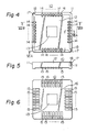
- Figures 4, 5, and 6 are a top plan view, a side view, and a bottom plan view of the holder 10, respectively.
- the holder 10 comprises a box-type holder body having a square-shaped bottom surface. The length of each side of the bottom surface is about 14 mm, for example.
- Reference numeral 11 is a side wall. Enclosed by the side wall 11, a recess portion 12 for removably accommodating the LCC 30 is formed. At the center of the recess portion 12 is a hole 13 for radiating heat. On the inner wall of the recess portion 12, a plurality of contact leads 14 are provided.
- the contact leads 14 are adapted to contact with the electrode pads 32 of the LCC 30 when the LCC 30 is accommodated in the recess portion 12. Each of the contact leads 14 has an end 15 exposed on the bottom surface 16. Each end 15 forms an electrode pad of this holder 10.
- the electrode pads 15 of the holder 10 are adapted to be connected by soldering to electrode pads of the package 20, as described in detail later.
- the holder 10 does not have any horizontally- projected lead pins of conventional holders. Through the non-projected electrode pads 15 exposed on the bottom surface of the holder 10, any other device may be connected. Accordingly, the advantage of the LCC 30, that is, the LCC 30 can be mounted on any semiconductor device with a high density, is not deteriorated even when the holder 10 is employed.
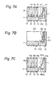
- FIG 7A is a partially expanded cross-sectional view taken along line VIIA-VIIA of Figure 4, when the holder 10 does not accommodate the LCC 30.
- each contact lead 14 has a spring means with contact portions 141 and 142 so that, when the LCC 30 is inserted into the recess portion 12, each of the contact leads 14 is pressed by the electrode pads 32 in the arrow direction, making sure that the electrode pads 32 are electrically in contact with the contact portions 141 and 142.
- Figure 7B illustrates the part of the cross-sectional view of the holder 10 when the LCC 30 is accommodated in the recess portion of the holder 10.
- the contact portions 141 and 142 are in surecontact with the electrode pad 32.
- the shape of the contact leads 14 is not restricted to the one illustrated in Figure 7A.
- Figure 7C illustrates another example of contact leads 14a having contact portions 141 a and 142a, which also ensures the electrical contact between the electrode pads 32 and the contact leads 14a.
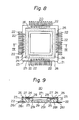
- Figure 8 is a top plan view of the package 20.
- the package 20 comprises a flat package body 21 and a plurality of horizontally extending pins 22 provided on the bottom surface of the flat package body 21.
- the flat package body 21 has a square-shaped main surface. On the main surface, there are provided a contact region 23 on the outermost portion of the main surface, a cap-covering region 24 on the inner portion of the contact region 23, and an inner-lead region 25 on the inner portion of the cap-covering region 24.
- Figure 9 is a cross-sectional view taken along line IX-IX of Figure 8.
- the contact region 23, the cap-covering region 24, and the inner-lead region 25 form a top step, a middle step, and a bottom step, respectively.
- a plurality of electrode pads 26 which are adapted to electrically contact by soldering the ends 15 of the contact leads 14, respectively, when the holder 10 is mounted on the package 20.
- a metal plate 27 is covered.
- a square-shaped cap 271 is fixed on the metal plate 27.
- each inner lead 28 is connected to either an electrode pad 26 or a pin 22.
- the flat package body 21 has several laminated ceramic layers. Between the laminated ceramic layers, the above-mentioned wiring layers are formed.
- the LCC 30 shown in Figure 3, the holder 10 shown in Figures 4 through 7, and the package 20 shown in Figures 8 and 9 are combined to form the evaluation one-chip microcomputer module as shown in Figure 2.
- the LCC 30 can be easily removed from the holder. Therefore, an erasing operation and rewriting operation can easily be carried out on the same EPROM. As a result, a desired program can be obtained at a low cost.
- Figure 10 is a general cross-sectional view of a semiconductor device module according to another embodiment of the present invention.
- a package 20a has an upside down configuration in comparison with the package 20 of Figure 9. That is, the semiconductor chip 29 is fixed in a recess portion formed, not in the top surface, but in the bottom surface of the package 20a.
- the holder 10 is mounted on the top surface of the package 20a by soldering.
- Reference character 22a represents pins of the package 20a.
- Reference numerals 271 and 291 represent the cap and the wire as in Figure 9.
- FIG 11 is a top plan view of the package 20a.
- a plurality of electrode pads 26a are provided on the top surface of the package 20a. These electrode pads 26a are adapted to electrically contact, by soldering, with the ends 15 of the contact leads 14 of the holder 10.
- the top surface of the package 20a in this embodiment is flat and does. not have the stair shape as illustrated in Figure 9. Therefore, the top surface of the package 20a can be freely used. Accordingly, various sizes of holders can be mounted on the package 20a.
- the present invention is not restricted to the above-described embodiments.
- a square-shaped flat package body and a holder having a square-bottom surface rectangular shapes are also possible.
- a flat package instead of employing a flat package, a dual-inline package is also possible.
- the present invention can be effectively applied to many other semiconductor devices when a part of the semiconductor elements in the device is after required to be replaced.
- an LCC since a holder for removably accommodating an LCC is obtained and since a semiconductor device module comprising the holder is obtained, an LCC can easily be removed from the semiconductor device module.
- an LCC includes an EPROM
- the EPROM can easily be rewritten at a low cost or the LCC can easily be replaced by another LCC at a low cost.
Landscapes
- Engineering & Computer Science (AREA)
- Microelectronics & Electronic Packaging (AREA)
- Physics & Mathematics (AREA)
- Condensed Matter Physics & Semiconductors (AREA)
- General Physics & Mathematics (AREA)
- Computer Hardware Design (AREA)
- Power Engineering (AREA)
- Structures For Mounting Electric Components On Printed Circuit Boards (AREA)
- Connecting Device With Holders (AREA)
Applications Claiming Priority (2)
| Application Number | Priority Date | Filing Date | Title |
|---|---|---|---|
| JP57089411A JPS58206147A (ja) | 1982-05-26 | 1982-05-26 | 半導体装置モジユ−ル |
| JP89411/82 | 1982-05-26 |
Publications (3)
| Publication Number | Publication Date |
|---|---|
| EP0095391A2 EP0095391A2 (en) | 1983-11-30 |
| EP0095391A3 EP0095391A3 (en) | 1985-10-09 |
| EP0095391B1 true EP0095391B1 (en) | 1988-05-18 |
Family
ID=13969898
Family Applications (1)
| Application Number | Title | Priority Date | Filing Date |
|---|---|---|---|
| EP83303053A Expired EP0095391B1 (en) | 1982-05-26 | 1983-05-26 | Mounting leadless chip-carriers |
Country Status (5)
| Country | Link |
|---|---|
| US (1) | US4737884A (OSRAM) |
| EP (1) | EP0095391B1 (OSRAM) |
| JP (1) | JPS58206147A (OSRAM) |
| DE (1) | DE3376711D1 (OSRAM) |
| IE (1) | IE54712B1 (OSRAM) |
Families Citing this family (11)
| Publication number | Priority date | Publication date | Assignee | Title |
|---|---|---|---|---|
| GB2164213B (en) * | 1984-09-06 | 1988-07-13 | Nec Corp | Structure for connecting leadless chip carrier |
| FR2590051B1 (fr) * | 1985-11-08 | 1991-05-17 | Eurotechnique Sa | Carte comportant un composant et micromodule a contacts de flanc |
| FR2590052B1 (fr) * | 1985-11-08 | 1991-03-01 | Eurotechnique Sa | Procede de recyclage d'une carte comportant un composant, carte prevue pour etre recyclee |
| EP0346061A3 (en) * | 1988-06-08 | 1991-04-03 | Fujitsu Limited | Integrated circuit device having an improved package structure |
| FR2634616B1 (fr) * | 1988-07-20 | 1995-08-25 | Matra | Procede de montage de micro-composants electroniques sur un support et produit realisable par le procede |
| USD317448S (en) | 1988-11-14 | 1991-06-11 | Transition Technology | Input/output module |
| US5054494A (en) * | 1989-12-26 | 1991-10-08 | U.S. Medical Corporation | Oscillometric blood pressure device |
| US5407360A (en) * | 1993-06-22 | 1995-04-18 | Berg Technology, Inc. | Connector for high density electronic assemblies |
| USD719537S1 (en) * | 2013-05-08 | 2014-12-16 | Mitsubishi Electric Corporation | Semiconductor device |
| DE112014003944B4 (de) * | 2013-08-30 | 2018-08-02 | Yazaki Corporation | Verbindungsstruktur eines elektronischen Bauelements und von Metallanschlussstücken |
| US20240206066A1 (en) * | 2022-12-20 | 2024-06-20 | Qualcomm Incorporated | Hybrid circuit board device to support circuit reuse and method of manufacture |
Family Cites Families (18)
| Publication number | Priority date | Publication date | Assignee | Title |
|---|---|---|---|---|
| US3479634A (en) * | 1967-10-25 | 1969-11-18 | Amp Inc | Printed circuit board connectors |
| US4356532A (en) * | 1980-07-18 | 1982-10-26 | Thomas & Betts Corporation | Electronic package and accessory component assembly |
| US3846734A (en) * | 1973-02-06 | 1974-11-05 | Amp Inc | Frames for adapting a multi-contact electrical connector to electrically connect with various styles of substrates |
| JPS5066168A (OSRAM) * | 1973-10-12 | 1975-06-04 | ||
| US4052118A (en) * | 1975-05-30 | 1977-10-04 | Amp Incorporated | Contact carrying spring member |
| US4035046A (en) * | 1976-01-15 | 1977-07-12 | Amp Incorporated | Miniature electrical connector for parallel panel members |
| US4037270A (en) * | 1976-05-24 | 1977-07-19 | Control Data Corporation | Circuit packaging and cooling |
| US4155615A (en) * | 1978-01-24 | 1979-05-22 | Amp Incorporated | Multi-contact connector for ceramic substrate packages and the like |
| JPS556124U (OSRAM) * | 1978-06-29 | 1980-01-16 | ||
| US4271426A (en) * | 1978-08-10 | 1981-06-02 | Minnesota Mining And Manufacturing Company | Leaded mounting and connector unit for an electronic device |
| US4278311A (en) * | 1979-04-06 | 1981-07-14 | Amp Incorporated | Surface to surface connector |
| US4330163A (en) * | 1979-12-05 | 1982-05-18 | E. I. Du Pont De Nemours And Company | Zero insertion force connector for LSI circuit package |
| AU6671681A (en) * | 1980-02-22 | 1981-08-27 | Amp Incorporated | Electrical connector |
| US4378139A (en) * | 1981-07-14 | 1983-03-29 | Wells Electronics, Inc. | Integrated circuit carrier connector |
| US4417777A (en) * | 1981-10-13 | 1983-11-29 | Molex Incorporated | Integrated circuit carrier assembly |
| JPS59132152A (ja) * | 1983-01-18 | 1984-07-30 | Japan Aviation Electronics Ind Ltd | セルフロツクコンタクト |
| US4558397A (en) * | 1983-12-19 | 1985-12-10 | Amp Incorporated | Interposer connector for surface mounting a ceramic chip carrier to a printed circuit board |
| US4627533A (en) * | 1984-10-29 | 1986-12-09 | Hughes Aircraft Company | Ceramic package for compensated crystal oscillator |
-
1982
- 1982-05-26 JP JP57089411A patent/JPS58206147A/ja active Granted
-
1983
- 1983-05-26 EP EP83303053A patent/EP0095391B1/en not_active Expired
- 1983-05-26 DE DE8383303053T patent/DE3376711D1/de not_active Expired
- 1983-05-26 IE IE1251/83A patent/IE54712B1/en not_active IP Right Cessation
-
1987
- 1987-06-24 US US07/065,668 patent/US4737884A/en not_active Expired - Fee Related
Also Published As
| Publication number | Publication date |
|---|---|
| DE3376711D1 (en) | 1988-06-23 |
| EP0095391A3 (en) | 1985-10-09 |
| JPH0226785B2 (OSRAM) | 1990-06-12 |
| US4737884A (en) | 1988-04-12 |
| EP0095391A2 (en) | 1983-11-30 |
| IE831251L (en) | 1983-11-26 |
| IE54712B1 (en) | 1990-01-17 |
| JPS58206147A (ja) | 1983-12-01 |
Similar Documents
| Publication | Publication Date | Title |
|---|---|---|
| US4371912A (en) | Method of mounting interrelated components | |
| EP0090633B1 (en) | Semiconductor device having radiator | |
| US5275975A (en) | Method of making a relatively flat semiconductor package having a semiconductor chip encapsulated in molded material | |
| US4026412A (en) | Electronic circuit carrier and test fixture | |
| US4458291A (en) | Package for enclosing semiconductor elements | |
| US4975763A (en) | Edge-mounted, surface-mount package for semiconductor integrated circuit devices | |
| EP0095391B1 (en) | Mounting leadless chip-carriers | |
| KR20000035363A (ko) | 그리드 어레이 형태의 접속 단자를 갖는 반도체 장치 | |
| US5324985A (en) | Packaged semiconductor device | |
| US6329594B1 (en) | Integrated circuit package | |
| JP2544976B2 (ja) | 半導体集積回路モジュ―ル | |
| US7126219B2 (en) | Small memory card | |
| US5291127A (en) | Chip-lifetime testing instrument for semiconductor devices | |
| KR920007209B1 (ko) | 집적회로 메모리 칩용 플래트 팩키지 | |
| JP2798593B2 (ja) | 半導体装置 | |
| KR960000216B1 (ko) | 메모리 카드 | |
| JP2618891B2 (ja) | メモリカートリツジ | |
| JP3024943B2 (ja) | Qfpプラスチック表面実装半導体電力装置 | |
| CA2036004A1 (en) | Semiconductor device storage jig | |
| JPH04237154A (ja) | 半導体パッケージ | |
| JP2796119B2 (ja) | 半導体デバイスおよびメモリモジュールデバイス | |
| KR100729052B1 (ko) | 반도체패키지 테스트용 범용 소켓 | |
| KR100246317B1 (ko) | 반도체 패키지 | |
| KR20060079428A (ko) | 칩 온 보드 패키지용 인쇄 회로 기판 및 이를 이용한 칩온 보드 패키지 | |
| JPS5911454Y2 (ja) | Ic用ソケツト |
Legal Events
| Date | Code | Title | Description |
|---|---|---|---|
| PUAI | Public reference made under article 153(3) epc to a published international application that has entered the european phase |
Free format text: ORIGINAL CODE: 0009012 |
|
| AK | Designated contracting states |
Designated state(s): DE FR GB |
|
| PUAL | Search report despatched |
Free format text: ORIGINAL CODE: 0009013 |
|
| AK | Designated contracting states |
Designated state(s): DE FR GB |
|
| 17P | Request for examination filed |
Effective date: 19860327 |
|
| 17Q | First examination report despatched |
Effective date: 19870804 |
|
| GRAA | (expected) grant |
Free format text: ORIGINAL CODE: 0009210 |
|
| AK | Designated contracting states |
Kind code of ref document: B1 Designated state(s): DE FR GB |
|
| REF | Corresponds to: |
Ref document number: 3376711 Country of ref document: DE Date of ref document: 19880623 |
|
| ET | Fr: translation filed | ||
| PLBE | No opposition filed within time limit |
Free format text: ORIGINAL CODE: 0009261 |
|
| STAA | Information on the status of an ep patent application or granted ep patent |
Free format text: STATUS: NO OPPOSITION FILED WITHIN TIME LIMIT |
|
| 26N | No opposition filed | ||
| PGFP | Annual fee paid to national office [announced via postgrant information from national office to epo] |
Ref country code: GB Payment date: 19930309 Year of fee payment: 11 |
|
| PGFP | Annual fee paid to national office [announced via postgrant information from national office to epo] |
Ref country code: DE Payment date: 19930724 Year of fee payment: 11 |
|
| PG25 | Lapsed in a contracting state [announced via postgrant information from national office to epo] |
Ref country code: GB Effective date: 19940526 |
|
| GBPC | Gb: european patent ceased through non-payment of renewal fee |
Effective date: 19940526 |
|
| PG25 | Lapsed in a contracting state [announced via postgrant information from national office to epo] |
Ref country code: DE Effective date: 19950201 |
|
| PGFP | Annual fee paid to national office [announced via postgrant information from national office to epo] |
Ref country code: FR Payment date: 19980511 Year of fee payment: 16 |
|
| PG25 | Lapsed in a contracting state [announced via postgrant information from national office to epo] |
Ref country code: FR Free format text: LAPSE BECAUSE OF NON-PAYMENT OF DUE FEES Effective date: 20000131 |
|
| REG | Reference to a national code |
Ref country code: FR Ref legal event code: ST |