EP0090135B1 - Semiconductor injection lasers - Google Patents
Semiconductor injection lasers Download PDFInfo
- Publication number
- EP0090135B1 EP0090135B1 EP83100522A EP83100522A EP0090135B1 EP 0090135 B1 EP0090135 B1 EP 0090135B1 EP 83100522 A EP83100522 A EP 83100522A EP 83100522 A EP83100522 A EP 83100522A EP 0090135 B1 EP0090135 B1 EP 0090135B1
- Authority
- EP
- European Patent Office
- Prior art keywords
- coating
- laser
- cleaved
- light output
- over
- Prior art date
- Legal status (The legal status is an assumption and is not a legal conclusion. Google has not performed a legal analysis and makes no representation as to the accuracy of the status listed.)
- Expired
Links
- 239000004065 semiconductor Substances 0.000 title claims description 15
- 238000002347 injection Methods 0.000 title claims description 7
- 239000007924 injection Substances 0.000 title claims description 7
- 238000000576 coating method Methods 0.000 claims description 43
- 239000011248 coating agent Substances 0.000 claims description 41
- 239000013078 crystal Substances 0.000 claims description 15
- 238000000137 annealing Methods 0.000 claims description 10
- 239000000463 material Substances 0.000 claims description 10
- 238000000034 method Methods 0.000 claims description 9
- 230000006798 recombination Effects 0.000 claims description 9
- 238000005215 recombination Methods 0.000 claims description 9
- 150000001875 compounds Chemical class 0.000 claims description 8
- 239000004615 ingredient Substances 0.000 claims description 5
- 229910001218 Gallium arsenide Inorganic materials 0.000 claims description 4
- 238000010438 heat treatment Methods 0.000 claims description 4
- 229910004613 CdTe Inorganic materials 0.000 claims description 2
- UHYPYGJEEGLRJD-UHFFFAOYSA-N cadmium(2+);selenium(2-) Chemical compound [Se-2].[Cd+2] UHYPYGJEEGLRJD-UHFFFAOYSA-N 0.000 claims description 2
- 238000000151 deposition Methods 0.000 claims description 2
- 230000015556 catabolic process Effects 0.000 description 10
- 238000006731 degradation reaction Methods 0.000 description 10
- 238000005452 bending Methods 0.000 description 4
- 238000001465 metallisation Methods 0.000 description 4
- 238000009792 diffusion process Methods 0.000 description 3
- KRHYYFGTRYWZRS-UHFFFAOYSA-N Fluorane Chemical compound F KRHYYFGTRYWZRS-UHFFFAOYSA-N 0.000 description 2
- 238000013459 approach Methods 0.000 description 2
- MVPPADPHJFYWMZ-UHFFFAOYSA-N chlorobenzene Chemical compound ClC1=CC=CC=C1 MVPPADPHJFYWMZ-UHFFFAOYSA-N 0.000 description 2
- 238000010586 diagram Methods 0.000 description 2
- 230000003287 optical effect Effects 0.000 description 2
- 239000000243 solution Substances 0.000 description 2
- 238000004544 sputter deposition Methods 0.000 description 2
- 229910052581 Si3N4 Inorganic materials 0.000 description 1
- 238000010521 absorption reaction Methods 0.000 description 1
- 230000015572 biosynthetic process Effects 0.000 description 1
- 239000000969 carrier Substances 0.000 description 1
- 230000001427 coherent effect Effects 0.000 description 1
- 230000008021 deposition Effects 0.000 description 1
- 239000011521 glass Substances 0.000 description 1
- 238000004519 manufacturing process Methods 0.000 description 1
- 239000002184 metal Substances 0.000 description 1
- 230000000737 periodic effect Effects 0.000 description 1
- 229920002120 photoresistant polymer Polymers 0.000 description 1
- 230000001681 protective effect Effects 0.000 description 1
- 238000007738 vacuum evaporation Methods 0.000 description 1
Images
Classifications
-
- H—ELECTRICITY
- H01—ELECTRIC ELEMENTS
- H01S—DEVICES USING THE PROCESS OF LIGHT AMPLIFICATION BY STIMULATED EMISSION OF RADIATION [LASER] TO AMPLIFY OR GENERATE LIGHT; DEVICES USING STIMULATED EMISSION OF ELECTROMAGNETIC RADIATION IN WAVE RANGES OTHER THAN OPTICAL
- H01S5/00—Semiconductor lasers
- H01S5/02—Structural details or components not essential to laser action
- H01S5/028—Coatings ; Treatment of the laser facets, e.g. etching, passivation layers or reflecting layers
- H01S5/0281—Coatings made of semiconductor materials
-
- H—ELECTRICITY
- H01—ELECTRIC ELEMENTS
- H01L—SEMICONDUCTOR DEVICES NOT COVERED BY CLASS H10
- H01L33/00—Semiconductor devices having potential barriers specially adapted for light emission; Processes or apparatus specially adapted for the manufacture or treatment thereof or of parts thereof; Details thereof
Definitions
- the present invention refers to semiconductor injection lasers wherein an input current is converted to a coherent light output.
- Injection lasers employ a semiconductor crystal of a binary or mixed compound of elements usually from group III and group V of the periodic table.
- a cleaved surface of the semiconductor crystal is employed as a partially reflecting mirror at the ends of the laser cavity.
- the cleaved mirror surface tends, in use, to degrade catastrophically when the laser operates at high current values and it degrades systematically when the laser is operated at lower current values. This degradation places a limit on the usefulness of the structure.
- the degradation at the cleaved light output surface of an injection laser is due to localized heating at the surface resulting from surface recombination of the carriers due to energy band bending at the cleaved surface of the semiconductor and that for an injection laser semiconductor crystal including GaAs, GaAIAs or GalnAsP as examples, a simple annealed coating of an optically transparent compound formed on the cleaved light output surface and having at least one ingredient thereof with a higher bandgap will not only reduce the degradation but also will increase the optical power density at which any degradation takes place.
- the annealed coating for example, may be of the group including ZnS, CdS, CdTe and CdSe.
- At least one ingredient of the coating material migrates and interacts with at least species or element of the laser crystal material responsible for the energy band bending.
- the annealing is conducted at a temperature sufficient to penetrate any oxide between the coating and the laser crystal yet the temperature should be lower than that which would damage the laser crystal or evaporate the coating.
- the annealing time should be less than would produce long range diffusion.
- a temperature range of from 400 to 800°K for 100 to 1000 minutes is considered satisfactory.
- FIG. 1 an energy band diagram is shown that illustrates the problem produced by the conditions at the cleaved light output surface.
- the cleaved crystal surface has properties which result in the bending of the energy bands as they approach the surface so that a carrier is induced to recombine. The energy released when recombination occurs is converted to heat at this localized region which damages the semiconductor.
- This invention is the control of degradation by providing a simple annealed coating on the cleaved light output surface.
- the annealed coating material has the properties of thickness for optical transparency and has at least one ingredient thereof with an energy bandgap that is largerthan that of the laser semiconductor crystal.
- the annealed coating material of the invention inhibits recombination and should be contrasted with the prior art approaches achieved by diffusion and epitaxial growth because while such regions do reduce the degradation, they require either the high temperatures of diffusion orthe lattice matching constraints of epitaxial growth and hence frequently interfere with other processing and structural arrangements.
- the lasing threshold current is usually increased and the reproducibility of the devices becomes more difficult since the region thickness adjacent to the cleaved light output surface becomes a critical parameter and is an additional parameter to control. Relaxation of the lattice matching consideration is a major advantage.
- the coating of the invention in contrast is simple, is placed over the cleaved surface and does not interfere with other processing requirements.
- the preferred embodiment of the invention is an annealed coating of an optically transparent compound having at least one element thereof with an energy bandgap that is larger than that of the laser semiconductor crystal.
- the annealed coating ZnS is applied to the ends of the laser active region.
- the coating may be applied by sputtering.
- the coating is in a thickness that is optically transparent of the order of 0.02 to 2 pm.
- the annealing is done by heating the GaAs laser with the ZnS coating over the cleaved light output surfaces for 100-1000 minutes at 600-800-K.
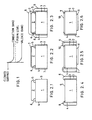
- the laser active region in Figs. 2.1-2.6 while only illustrated to the detail needed for the invention may also include a heterojunction bounded cavity as is standard practice in the art.
- a process of providing the structure of Fig. 2.6 is shown in Figs. 2.1 through 2.6 wherein the coating over the cleaved surfaces and subsequent annealing, can take place prior to the application of the contacts.
- a body 1 which is a cleaved laser or in the alternative a row of cleaved lasers.
- a mask 2 such as a positive photoresist is applied but set back from each cleaved light output surface 3 and 4 in areas 5 and 6, respectively.
- the mask 2 is usually applied prior to the cleaving of the surfaces 3 and 4.
- Providing the mask 2 with an overhang such as by a chlorobenzene soak type process will facilitate later steps where materials are to be kept off areas 5 and 6.
- a coating 7 of the material ZnS is applied evenly over the areas by a directional deposition that prevents covering the areas 5 and 6.
- the process of sputtering at room temperature operates satisfactorily for this purpose. It is helpful if the coating covers only the cleaved mirror surfaces 3 and 4 and the mask2 but is not continuous overthe sides of the mask 2 and into the regions 5 and 6. An overhang on the mask facilitates this.
- the function of the coating 8 will be to delineate ohmic contact areas to be added later.
- any thermal annealing steps found desirable for the particular coating material 7 are to be conducted so that the annealing temperature will not affect or degrade the ohmic contacts since at this pointthey have not been applied.
- a metallization coating is applied such as by the process of vacuum evaporation.
- the metallization operation provides a coating 10 which also covers the thick coatings 8 and is in contact with the surface 9.
- a separate ohmic contact 11 is also made to the surface opposite to the surface 9 either in the same metallization or in a separate operation.
- the final device is illustrated in Fig. 2.6 wherein the technique of "lift-off" standard in the art is employed.
- the "lift-off” technique relies on the removal of support from a coating so that the coating literally breaks at a desired point.
- the coating 8 is dissolved in an etchant such as hydrofluoric acid so that the metallization 10 over the coating 8 breaks at the intersection with the surface 9.
- the coating 8 and the metat 10thereover on each cleaved surface is lifted off and the structure of Fig. 2.6 is the result.
- the remaining metal 10 in contact with the surface 9 is one ohmic device contact and the other ohmic device contact 11.
- the annealing coatings 7 on each cleaved light output surface serve as surface recombination controlling windows over those cleaved surfaces 3 and 4.
Landscapes
- Physics & Mathematics (AREA)
- Engineering & Computer Science (AREA)
- Condensed Matter Physics & Semiconductors (AREA)
- General Physics & Mathematics (AREA)
- Electromagnetism (AREA)
- Optics & Photonics (AREA)
- Manufacturing & Machinery (AREA)
- Computer Hardware Design (AREA)
- Microelectronics & Electronic Packaging (AREA)
- Power Engineering (AREA)
- Semiconductor Lasers (AREA)
Applications Claiming Priority (2)
| Application Number | Priority Date | Filing Date | Title |
|---|---|---|---|
| US06/363,193 US4751708A (en) | 1982-03-29 | 1982-03-29 | Semiconductor injection lasers |
| US363193 | 1994-12-22 |
Publications (2)
| Publication Number | Publication Date |
|---|---|
| EP0090135A1 EP0090135A1 (en) | 1983-10-05 |
| EP0090135B1 true EP0090135B1 (en) | 1987-07-08 |
Family
ID=23429216
Family Applications (1)
| Application Number | Title | Priority Date | Filing Date |
|---|---|---|---|
| EP83100522A Expired EP0090135B1 (en) | 1982-03-29 | 1983-01-21 | Semiconductor injection lasers |
Country Status (4)
| Country | Link |
|---|---|
| US (1) | US4751708A (ja) |
| EP (1) | EP0090135B1 (ja) |
| JP (1) | JPS58171881A (ja) |
| DE (1) | DE3372431D1 (ja) |
Families Citing this family (11)
| Publication number | Priority date | Publication date | Assignee | Title |
|---|---|---|---|---|
| US4840922A (en) * | 1986-07-29 | 1989-06-20 | Ricoh Company, Ltd. | Method of manufacturing masked semiconductor laser |
| JPS63198390A (ja) * | 1987-02-13 | 1988-08-17 | Ricoh Co Ltd | マスク半導体レ−ザ−の製作方法 |
| NL8700904A (nl) * | 1987-04-16 | 1988-11-16 | Philips Nv | Halfgeleiderlaserinrichting en werkwijze voor het vervaardigen daarvan. |
| US4828935A (en) * | 1988-03-30 | 1989-05-09 | The United States Of America As Represented By The Secretary Of The Navy | Passivating layer for III-V semiconductor materials |
| US4910166A (en) * | 1989-01-17 | 1990-03-20 | General Electric Company | Method for partially coating laser diode facets |
| JPH0834337B2 (ja) * | 1990-04-02 | 1996-03-29 | シャープ株式会社 | 半導体レーザ素子の製造方法 |
| JP2941364B2 (ja) * | 1990-06-19 | 1999-08-25 | 株式会社東芝 | 半導体レーザ装置 |
| JP3672106B2 (ja) * | 1994-09-28 | 2005-07-13 | シャープ株式会社 | 端面成長窓型半導体レーザ素子の製造方法 |
| US5665637A (en) * | 1995-11-17 | 1997-09-09 | Lucent Technologies Inc. | Passivated faceted article comprising a semiconductor laser |
| JPH09167873A (ja) * | 1995-12-15 | 1997-06-24 | Mitsubishi Electric Corp | 半導体レーザ装置 |
| DE10312214B4 (de) * | 2003-03-19 | 2008-11-20 | Osram Opto Semiconductors Gmbh | Verfahren zum Herstellen von mindestens einer Mesa- oder Stegstruktur oder von mindestens einem elektrisch gepumpten Bereich in einer Schicht oder Schichtenfolge |
Family Cites Families (9)
| Publication number | Priority date | Publication date | Assignee | Title |
|---|---|---|---|---|
| JPS5527474B2 (ja) * | 1971-12-17 | 1980-07-21 | ||
| US3849738A (en) * | 1973-04-05 | 1974-11-19 | Bell Telephone Labor Inc | Multilayer antireflection coatings for solid state lasers |
| US4062035A (en) * | 1975-02-05 | 1977-12-06 | Siemens Aktiengesellschaft | Luminescent diode |
| US4001719A (en) * | 1975-08-13 | 1977-01-04 | Bell Telephone Laboratories, Incorporated | Fabrication of a self-aligned mirror on a solid-state laser for controlling filamentation |
| US4178564A (en) * | 1976-01-15 | 1979-12-11 | Rca Corporation | Half wave protection layers on injection lasers |
| CA1115401A (en) * | 1977-10-11 | 1981-12-29 | Peter A. Barnes | Glass coating for semiconductor optical devices |
| JPS5527474A (en) * | 1978-08-19 | 1980-02-27 | Arata Kogyosho:Kk | Manufacture of spherical head for use of oiler or the like of diesel engine |
| NL7903197A (nl) * | 1979-04-24 | 1980-10-28 | Philips Nv | Werkwijze voor het vervaardigen van een elektrolumines- cerende halfgeleiderinrichting en elektroluminescerende halfgeleiderinrichting vervaardigd volgens de werkwijze |
| US4354198A (en) * | 1980-05-30 | 1982-10-12 | International Business Machines Corporation | Zinc-sulphide capping layer for gallium-arsenide device |
-
1982
- 1982-03-29 US US06/363,193 patent/US4751708A/en not_active Expired - Fee Related
- 1982-11-17 JP JP57200513A patent/JPS58171881A/ja active Granted
-
1983
- 1983-01-21 DE DE8383100522T patent/DE3372431D1/de not_active Expired
- 1983-01-21 EP EP83100522A patent/EP0090135B1/en not_active Expired
Non-Patent Citations (2)
| Title |
|---|
| JAPANESE JOURNAL OF APPLIED PHYSICS, vol. 17, no. 5, May 1978, pages 865-870, Tokyo, JP. S. TAKAHASHI et al.: "GaAs-A1GaAs DH lasers with buried facet" * |
| JOURNAL OF APPLIED PHYSICS, vol. 50, no. 8, August 1979, pages 5150-5157, New York, USA H. YONEZY et al.: "Mirror degradation in A1GaAs double-heterostructure lasers" * |
Also Published As
| Publication number | Publication date |
|---|---|
| DE3372431D1 (en) | 1987-08-13 |
| JPS6348438B2 (ja) | 1988-09-29 |
| US4751708A (en) | 1988-06-14 |
| EP0090135A1 (en) | 1983-10-05 |
| JPS58171881A (ja) | 1983-10-08 |
Similar Documents
| Publication | Publication Date | Title |
|---|---|---|
| US4639275A (en) | Forming disordered layer by controlled diffusion in heterojunction III-V semiconductor | |
| US4511408A (en) | Semiconductor device fabrication with disordering elements introduced into active region | |
| US4594603A (en) | Semiconductor device with disordered active region | |
| CA1102903A (en) | Fabrication of mesa devices by mbe growth over channeled substrates | |
| US4654090A (en) | Selective disordering of well structures by laser annealing | |
| EP0090135B1 (en) | Semiconductor injection lasers | |
| US5933705A (en) | Passivation and protection of semiconductor surface | |
| US5019519A (en) | Method for the manufacture of optical semiconductor device | |
| US3654497A (en) | Semiconductor lasers utilizing internal saturable absorbers | |
| Mito et al. | InGaAsP planar buried heterostructure laser diode (PBH-LD) with very low threshold current | |
| EP0077825B1 (en) | Method of forming wide bandgap region within multilayer semiconductors | |
| KR900003844B1 (ko) | 반도체 레이저장치와 그 제조방법 | |
| US4439004A (en) | Optical waveguide and modulator and process for fabricating same | |
| EP1058359B1 (en) | Compound semiconductor surface stabilizing method | |
| US5010375A (en) | Semiconductor laser device | |
| JPS58170069A (ja) | 3−v族化合物半導体装置 | |
| USRE33274E (en) | Selective disordering of well structures by laser annealing | |
| EP0388149A2 (en) | A semiconductor laser device and a method for the production of the same | |
| JP2757915B2 (ja) | Ii−vi族半導体デバイス及びその製造方法 | |
| GB2109155A (en) | Semiconductor laser manufacture | |
| US20040032893A1 (en) | Passivation of the resonator end faces of semiconductor lasers based on iii-v semiconductor material | |
| US4725450A (en) | Method for fabricating a semiconductor laser device | |
| JPH05129721A (ja) | 半導体レーザー及びその製造方法 | |
| KR0146711B1 (ko) | 인화합물 형성에 의한 표면방출 레이저 다이오드 공진표면의 비활성화 방법 | |
| GB2079524A (en) | Semiconductor laser |
Legal Events
| Date | Code | Title | Description |
|---|---|---|---|
| PUAI | Public reference made under article 153(3) epc to a published international application that has entered the european phase |
Free format text: ORIGINAL CODE: 0009012 |
|
| AK | Designated contracting states |
Designated state(s): DE FR GB |
|
| 17P | Request for examination filed |
Effective date: 19840126 |
|
| GRAA | (expected) grant |
Free format text: ORIGINAL CODE: 0009210 |
|
| AK | Designated contracting states |
Kind code of ref document: B1 Designated state(s): DE FR GB |
|
| REF | Corresponds to: |
Ref document number: 3372431 Country of ref document: DE Date of ref document: 19870813 |
|
| ET | Fr: translation filed | ||
| PLBE | No opposition filed within time limit |
Free format text: ORIGINAL CODE: 0009261 |
|
| STAA | Information on the status of an ep patent application or granted ep patent |
Free format text: STATUS: NO OPPOSITION FILED WITHIN TIME LIMIT |
|
| 26N | No opposition filed | ||
| PGFP | Annual fee paid to national office [announced via postgrant information from national office to epo] |
Ref country code: GB Payment date: 19911206 Year of fee payment: 10 |
|
| PG25 | Lapsed in a contracting state [announced via postgrant information from national office to epo] |
Ref country code: GB Effective date: 19930121 |
|
| GBPC | Gb: european patent ceased through non-payment of renewal fee |
Effective date: 19930121 |
|
| PGFP | Annual fee paid to national office [announced via postgrant information from national office to epo] |
Ref country code: FR Payment date: 19941223 Year of fee payment: 13 |
|
| PGFP | Annual fee paid to national office [announced via postgrant information from national office to epo] |
Ref country code: DE Payment date: 19950117 Year of fee payment: 13 |
|
| PG25 | Lapsed in a contracting state [announced via postgrant information from national office to epo] |
Ref country code: FR Effective date: 19960930 |
|
| PG25 | Lapsed in a contracting state [announced via postgrant information from national office to epo] |
Ref country code: DE Effective date: 19961001 |
|
| REG | Reference to a national code |
Ref country code: FR Ref legal event code: ST |