EP0089452B1 - Hörgerät mit einer Verstärkerschaltung - Google Patents
Hörgerät mit einer Verstärkerschaltung Download PDFInfo
- Publication number
- EP0089452B1 EP0089452B1 EP83100082A EP83100082A EP0089452B1 EP 0089452 B1 EP0089452 B1 EP 0089452B1 EP 83100082 A EP83100082 A EP 83100082A EP 83100082 A EP83100082 A EP 83100082A EP 0089452 B1 EP0089452 B1 EP 0089452B1
- Authority
- EP
- European Patent Office
- Prior art keywords
- printed circuit
- circuit board
- carrier
- chassis
- circuit boards
- Prior art date
- Legal status (The legal status is an assumption and is not a legal conclusion. Google has not performed a legal analysis and makes no representation as to the accuracy of the status listed.)
- Expired
Links
Images
Classifications
-
- H—ELECTRICITY
- H05—ELECTRIC TECHNIQUES NOT OTHERWISE PROVIDED FOR
- H05K—PRINTED CIRCUITS; CASINGS OR CONSTRUCTIONAL DETAILS OF ELECTRIC APPARATUS; MANUFACTURE OF ASSEMBLAGES OF ELECTRICAL COMPONENTS
- H05K3/00—Apparatus or processes for manufacturing printed circuits
- H05K3/36—Assembling printed circuits with other printed circuits
- H05K3/366—Assembling printed circuits with other printed circuits substantially perpendicularly to each other
-
- H—ELECTRICITY
- H04—ELECTRIC COMMUNICATION TECHNIQUE
- H04R—LOUDSPEAKERS, MICROPHONES, GRAMOPHONE PICK-UPS OR LIKE ACOUSTIC ELECTROMECHANICAL TRANSDUCERS; ELECTRIC HEARING AIDS; PUBLIC ADDRESS SYSTEMS
- H04R25/00—Electric hearing aids
- H04R25/60—Mounting or interconnection of hearing aid parts, e.g. inside tips, housings or to ossicles
- H04R25/609—Mounting or interconnection of hearing aid parts, e.g. inside tips, housings or to ossicles of circuitry
-
- H—ELECTRICITY
- H04—ELECTRIC COMMUNICATION TECHNIQUE
- H04R—LOUDSPEAKERS, MICROPHONES, GRAMOPHONE PICK-UPS OR LIKE ACOUSTIC ELECTROMECHANICAL TRANSDUCERS; ELECTRIC HEARING AIDS; PUBLIC ADDRESS SYSTEMS
- H04R25/00—Electric hearing aids
- H04R25/60—Mounting or interconnection of hearing aid parts, e.g. inside tips, housings or to ossicles
- H04R25/603—Mounting or interconnection of hearing aid parts, e.g. inside tips, housings or to ossicles of mechanical or electronic switches or control elements
-
- H—ELECTRICITY
- H05—ELECTRIC TECHNIQUES NOT OTHERWISE PROVIDED FOR
- H05K—PRINTED CIRCUITS; CASINGS OR CONSTRUCTIONAL DETAILS OF ELECTRIC APPARATUS; MANUFACTURE OF ASSEMBLAGES OF ELECTRICAL COMPONENTS
- H05K2201/00—Indexing scheme relating to printed circuits covered by H05K1/00
- H05K2201/04—Assemblies of printed circuits
- H05K2201/048—Second PCB mounted on first PCB by inserting in window or holes of the first PCB
-
- H—ELECTRICITY
- H05—ELECTRIC TECHNIQUES NOT OTHERWISE PROVIDED FOR
- H05K—PRINTED CIRCUITS; CASINGS OR CONSTRUCTIONAL DETAILS OF ELECTRIC APPARATUS; MANUFACTURE OF ASSEMBLAGES OF ELECTRICAL COMPONENTS
- H05K2201/00—Indexing scheme relating to printed circuits covered by H05K1/00
- H05K2201/09—Shape and layout
- H05K2201/09145—Edge details
- H05K2201/09172—Notches between edge pads
-
- H—ELECTRICITY
- H05—ELECTRIC TECHNIQUES NOT OTHERWISE PROVIDED FOR
- H05K—PRINTED CIRCUITS; CASINGS OR CONSTRUCTIONAL DETAILS OF ELECTRIC APPARATUS; MANUFACTURE OF ASSEMBLAGES OF ELECTRICAL COMPONENTS
- H05K2201/00—Indexing scheme relating to printed circuits covered by H05K1/00
- H05K2201/09—Shape and layout
- H05K2201/09209—Shape and layout details of conductors
- H05K2201/095—Conductive through-holes or vias
- H05K2201/09645—Patterning on via walls; Plural lands around one hole
Definitions
- the invention is based on a hearing aid according to the preamble of the main claim.
- a hearing aid to be worn behind the ear is already known (Hearing Aid Journal, October 1980, page 14), in which several thick-film circuits perpendicular to it are arranged on a chassis-like circuit board arranged in the hearing device, the pin-shaped contacts of which are inserted into corresponding sockets on the circuit board are, which are connected to conductor tracks of the circuit board.
- Sockets and plug pins are relatively expensive, and possibly direct soldering of the thick-film circuits into a circuit board would make it difficult to replace the circuit in the event of a repair.
- this type of circuit requires a complicated manufacturing process.
- a hearing device contains a main circuit board onto which circuit board assemblies can be plugged.
- circuit board assemblies can be plugged.
- a certain combination is put together from a number of different circuit board components.
- the hearing aid concept explained above has proven itself for pocket hearing aids, but is technologically very complex and, for example, can hardly be used for hearing aids to be worn behind the ear for reasons of space.
- FR-A-24 42 570 it is also known (FR-A-24 42 570) to provide line crossings for a printed circuit which, instead of a simple wire bridge, which is to bridge a conductor path of a single-sided or double-sided laminated first printed circuit board, a second printed circuit board fastened vertically on the first plate is provided with a printed conduit. If several conductor tracks of the first printed circuit board are to be bridged, a single printed circuit board can have several bridges realized by conductor tracks.
- the second circuit board can also serve as a carrier for electrical components.
- the second printed circuit board can carry lugs at the connection point to the first printed circuit board, but they only have the purpose that there is space for a conductive path of the first printed circuit board to be bridged between two adjacent lugs.
- the hearing aid according to the invention with the characterizing features of the patent claim has the advantage that simple circuit boards that are laminated on both sides can be used as carriers for the amplifier circuit and that through the tongue-shaped projections, each carrying a connection element, which fit into an opening of the chassis circuit board, a particularly simple connection between the chassis circuit board and the carrier circuit boards is achieved.
- the carrier printed circuit boards are preferably equipped with electrical components that are customary in thin and thick-film circuits. Instead of the resistive layers applied to a substrate in thin and thick-film circuits, discrete chip resistors are preferably used in the hearing device according to the invention. Soldering the carrier circuit boards out of the chassis circuit board presents no problem for the person skilled in the art.
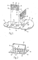
- the chassis circuit board 10 which is approximately matched to the external shape of a hearing aid to be worn behind the ear, is provided on one side or on both sides with conductor tracks 13 and 14 and contains slot-like openings 15, 16 and 17. Furthermore, the chassis circuit board 10 serves as a carrier for an adjusting resistor, of which only the adjusting wheel 18 can be seen in FIG. 1, and for a switch whose switching lever is designated 19.
- the carrier circuit board 11 is approximately U-shaped and carries conductor tracks 20 on both sides.
- the free ends of the U-shaped carrier circuit board 11 form tongues 21 and 22 which fit into openings 15 and 16 of the chassis circuit board 10.
- the free ends of the conductor tracks serving as connection elements 23 are electrically connected to the conductor tracks 14 of the chassis circuit board 10, for example by soldering.
- the electrical components 24, 25, 26 to be arranged on the carrier circuit board 11 are discrete electrical components, such as capacitors, resistors and transistors, the connections of which are connected to corresponding conductor tracks 20 by soldering.
- the carrier circuit board 12 is constructed in an analogous manner, the ends of conductor tracks 31 serving as connection elements 30 being arranged on a projection 32 of the carrier circuit board 12.
- the projection 32 fits into the slot-shaped opening 17 of the carrier circuit board 10.
- the invention relates to new photosensitive polymers, a process for their preparation, new anthraquinone derivatives that can be used, and the use of the new photosensitive polymers, especially +30
- Electrically conductive coatings and patterns, especially for printed circuits, can be produced, inter alia, by producing suitable zero-valued metal nuclei on non-conductive inorganic or organic substrates for electroless metal deposition. According to the so-called photoformation process, this can be done by scanning the substrate, optionally in an acidic medium and in the presence of halide ions, metal salts, especially salts of non-noble metals such as copper formate, and then by irradiation, if appropriate in the presence of chemical reducing agents , reduced to zero-value metal germs.
- Photosensitive reducing agents, a second reducing agent and a surface-active agent are generally used for the reduction of the metal salts. As light-sensitive reducing agents, i.a.
- Anthraquinone disulfonic acids and salts thereof, optionally in a mixture with metal activators such as tin salts, can be used.
- the substrates generally have to be etched before the metal deposition or provided with an etchable adhesion promoter layer [intramolecular photoreductive method; see. e.g. U.S. Patents 3,959,547 and 3,993,802].
- a photosensitive layer containing titanium dioxide is produced on the non-conductive substrate, or titanium dioxide is incorporated into the substrate.
- the substrate containing the titanium dioxide or the layer containing the titanium dioxide must then be etched in order to make the TiO 2 particles accessible for further treatment.
- the etched material is then treated with a solution of the desired metal salt and irradiated (photoelectron method).
- zero-valent metal nuclei can also be obtained by first depositing a light-sensitive metal salt, such as tin (II) hydroxide or iron oxalate, on the non-conductive substrate, producing a latent image or reducing metal ions by irradiation and then by reducing a metal salt, in general of a precious metal salt that generates zero-valent metal nuclei (photoelectrochemical method).
- a light-sensitive metal salt such as tin (II) hydroxide or iron oxalate
- reducing a metal salt in general of a precious metal salt that generates zero-valent metal nuclei (photoelectrochemical method).
- the zero-valent metal nuclei obtained in this way can then be metallized in a manner known per se by electroless metal deposition and the conductive image areas can be further reinforced, if necessary, by electrolytic metal deposition.
- New light-sensitive polymers have now been found, with which images, particularly electrically conductive coatings and patterns, can be produced in a much simpler and more economical manner, without the need to etch the substrate or to use etchable adhesive layers. Images created with the new polymers are also characterized by increased resolving power.
- the invention thus relates to new polymers with an intrinsic viscosity [ ⁇ ] of at least 0.10 dl / g, measured at 25 ° CN, N-dimethylformamide, which consist of 1 to 40 mol% recurring structural elements of the formula I FIG01 / 90mm and 60 to 99 mol% of repeating structural elements of the formula 11
- the carrier circuit board 11 preferably carries the components of a preamplifier or a control unit
- the carrier circuit board 12 has the electrical components for the output amplifier of the amplifier circuit.
- a carrier circuit board 40 has incisions 42 in its edge region 41 at regular intervals, through which tongue-shaped projections 43, each with a connecting element 44, are created.
- the protrusions fit into preferably plated-through openings 45 of a chassis circuit board 46, which is similar to the chassis circuit board 10 in FIG. 1. If the carrier circuit board 40 is inserted with its tongues 44 into the openings 45 of the chassis circuit board 46, the connection elements 44 can be connected to conductor tracks 47 on the underside of the chassis circuit board by dip soldering.
Landscapes
- Engineering & Computer Science (AREA)
- Otolaryngology (AREA)
- Microelectronics & Electronic Packaging (AREA)
- Health & Medical Sciences (AREA)
- General Health & Medical Sciences (AREA)
- Neurosurgery (AREA)
- Manufacturing & Machinery (AREA)
- Physics & Mathematics (AREA)
- Acoustics & Sound (AREA)
- Signal Processing (AREA)
- Combinations Of Printed Boards (AREA)
- Amplifiers (AREA)
- Mounting Of Printed Circuit Boards And The Like (AREA)
Priority Applications (1)
| Application Number | Priority Date | Filing Date | Title |
|---|---|---|---|
| AT83100082T ATE19171T1 (de) | 1982-03-18 | 1983-01-07 | Hoergeraet mit einer verstaerkerschaltung. |
Applications Claiming Priority (2)
| Application Number | Priority Date | Filing Date | Title |
|---|---|---|---|
| DE3209914 | 1982-03-18 | ||
| DE19823209914 DE3209914A1 (de) | 1982-03-18 | 1982-03-18 | Hoergeraet mit einer verstaerkerschaltung |
Publications (2)
| Publication Number | Publication Date |
|---|---|
| EP0089452A1 EP0089452A1 (de) | 1983-09-28 |
| EP0089452B1 true EP0089452B1 (de) | 1986-04-09 |
Family
ID=6158625
Family Applications (1)
| Application Number | Title | Priority Date | Filing Date |
|---|---|---|---|
| EP83100082A Expired EP0089452B1 (de) | 1982-03-18 | 1983-01-07 | Hörgerät mit einer Verstärkerschaltung |
Country Status (5)
| Country | Link |
|---|---|
| EP (1) | EP0089452B1 (da) |
| JP (1) | JPS58175399A (da) |
| AT (1) | ATE19171T1 (da) |
| DE (2) | DE3209914A1 (da) |
| DK (1) | DK80383A (da) |
Cited By (1)
| Publication number | Priority date | Publication date | Assignee | Title |
|---|---|---|---|---|
| CN104955272A (zh) * | 2014-03-31 | 2015-09-30 | 奇点新源国际技术开发(北京)有限公司 | 一种印刷电路板 |
Families Citing this family (24)
| Publication number | Priority date | Publication date | Assignee | Title |
|---|---|---|---|---|
| DE8428488U1 (de) * | 1984-09-27 | 1986-01-23 | Siemens AG, 1000 Berlin und 8000 München | Kleinhörgerät |
| FR2591054B1 (fr) * | 1985-08-29 | 1989-05-12 | Merlin Gerin | Montage de cartes de circuit imprime |
| DE8708893U1 (de) * | 1987-06-26 | 1988-10-27 | Siemens AG, 1000 Berlin und 8000 München | Hörgerät mit Leiterplatte |
| FI84214C (fi) * | 1987-08-21 | 1991-10-25 | Nokia Mobira Oy | Anordning foer anslutning av en hybridkrets till en basplatta. |
| DE8804743U1 (de) * | 1988-04-11 | 1989-08-10 | Siemens AG, 1000 Berlin und 8000 München | Hörhilfegerät, insbesondere Hörgerät mit einem hinter dem Ohr zu tragenden Gehäuse |
| DE3919273C2 (de) * | 1989-06-13 | 1993-10-14 | Bosch Gmbh Robert | Leiterplattenanordnung |
| DE8907230U1 (de) * | 1989-06-13 | 1989-09-21 | Robert Bosch Gmbh, 7000 Stuttgart | Elektronisches Gerät mit einer Leiterplattenanordnung |
| US5343366A (en) * | 1992-06-24 | 1994-08-30 | International Business Machines Corporation | Packages for stacked integrated circuit chip cubes |
| JPH06196833A (ja) * | 1992-12-25 | 1994-07-15 | Kenwood Corp | プリント基板取付け構造 |
| JPH0818188A (ja) * | 1994-06-29 | 1996-01-19 | Nec Niigata Ltd | コネクタレスプリント基板接続機構 |
| DE29617021U1 (de) * | 1996-09-30 | 1996-11-14 | Hella Kg Hueck & Co, 59557 Lippstadt | Leiterplatte |
| DE19640684A1 (de) * | 1996-10-02 | 1998-04-09 | Teves Gmbh Alfred | Mikroschalteranordnung für Bedienelemente von Kraftahrzeugschaltern |
| US6882538B1 (en) * | 1999-05-31 | 2005-04-19 | Tyco Electronics Logistics Ag | Intelligent power module |
| FR2818869B1 (fr) * | 2000-12-21 | 2003-09-19 | Thomson Csf | Cartes de circuit imprime pour enfichage securise carte a carte perpendiculaires |
| DE102006021023A1 (de) * | 2006-04-28 | 2007-10-31 | Würth Elektronik Rot am See GmbH & Co. KG | Baugruppenaufbau |
| US7864544B2 (en) | 2007-08-01 | 2011-01-04 | Delphi Technologies, Inc. | Printed circuit board assembly |
| DE102008012443B4 (de) * | 2008-03-04 | 2015-05-21 | Ifm Electronic Gmbh | Verbindungsanordnung zweier Leiterplatten für einen optischen Näherungsschalter |
| EP2321980B1 (en) * | 2008-09-11 | 2019-02-27 | Sivantos Pte. Ltd. | Hearing aid |
| ITMI20092018A1 (it) * | 2009-11-17 | 2011-05-18 | Dinema S P A | Procedimento di realizzazione di circuiti stampati ad elevata automazione. |
| GB2494919B (en) * | 2011-09-23 | 2015-06-17 | Control Tech Ltd | Method for connecting printed circuit boards. |
| DE102013108535A1 (de) * | 2013-08-07 | 2015-02-12 | SMR Patents S.à.r.l. | Verfahren zum Herstellen einer Platine, Platine und Rückblickvorrichtung |
| US10555415B2 (en) | 2013-08-07 | 2020-02-04 | SMR Patents S.à.r.l. | Method for manufacturing a printed circuit board |
| US10277996B2 (en) | 2015-12-01 | 2019-04-30 | Gn Hearing A/S | Hearing aid with a flexible carrier antenna and related method |
| JP6947657B2 (ja) * | 2018-01-31 | 2021-10-13 | 株式会社デンソー | 電子回路 |
Family Cites Families (5)
| Publication number | Priority date | Publication date | Assignee | Title |
|---|---|---|---|---|
| DE1054515B (de) * | 1956-04-26 | 1959-04-09 | Fuba Fabrikation Funktechnisch | Gedruckte Verdrahtung oder gedruckte Schaltung mit Leitungskreuzungen |
| GB1111887A (en) * | 1965-03-26 | 1968-05-01 | Danavox Internat A S | Hearing aid circuit module |
| JPS529057B2 (da) * | 1972-06-08 | 1977-03-14 | ||
| FR2442570A1 (fr) * | 1978-11-27 | 1980-06-20 | Radiotechnique Compelec | Procede d'insertion d'une plaque portant des plages de contact metallisees dans un substrat de circuits imprimes et dispositif obtenu |
| DE2941951A1 (de) * | 1979-10-17 | 1981-04-30 | Robert Bosch Gmbh, 7000 Stuttgart | Hoergeraet mit einer leiterplatte als traeger fuer leitungsbahnen sowie elektrische und mechanische bauelemente und baustufen |
-
1982
- 1982-03-18 DE DE19823209914 patent/DE3209914A1/de not_active Withdrawn
-
1983
- 1983-01-07 DE DE8383100082T patent/DE3362827D1/de not_active Expired
- 1983-01-07 EP EP83100082A patent/EP0089452B1/de not_active Expired
- 1983-01-07 AT AT83100082T patent/ATE19171T1/de not_active IP Right Cessation
- 1983-02-23 DK DK80383A patent/DK80383A/da not_active Application Discontinuation
- 1983-03-16 JP JP58042502A patent/JPS58175399A/ja active Pending
Cited By (1)
| Publication number | Priority date | Publication date | Assignee | Title |
|---|---|---|---|---|
| CN104955272A (zh) * | 2014-03-31 | 2015-09-30 | 奇点新源国际技术开发(北京)有限公司 | 一种印刷电路板 |
Also Published As
| Publication number | Publication date |
|---|---|
| EP0089452A1 (de) | 1983-09-28 |
| ATE19171T1 (de) | 1986-04-15 |
| DE3362827D1 (en) | 1986-05-15 |
| DE3209914A1 (de) | 1983-09-29 |
| DK80383A (da) | 1983-09-19 |
| JPS58175399A (ja) | 1983-10-14 |
| DK80383D0 (da) | 1983-02-23 |
Similar Documents
| Publication | Publication Date | Title |
|---|---|---|
| EP0089452B1 (de) | Hörgerät mit einer Verstärkerschaltung | |
| DE69125233T2 (de) | Verfahren zur Herstellung von gedruckten Schaltungen | |
| DE2856954C2 (da) | ||
| DE102004045451B4 (de) | Galvanisches Verfahren zum Füllen von Durchgangslöchern mit Metallen, insbesondere von Leiterplatten mit Kupfer | |
| DE19650296A1 (de) | Verfahren zum Herstellen eines Halbleiterbauelements | |
| DE3502744C2 (da) | ||
| EP0549791B1 (de) | Mehrlagenleiterplatte und verfahren zu ihrer herstellung | |
| DE69530698T2 (de) | Verfahren zur herstellung einer leiterplatte | |
| DE3045280C2 (de) | Verfahren zur Bildung von elektrischen Leiterbahnen auf einem isolierenden Substrat | |
| DE2251829A1 (de) | Verfahren zur herstellung metallisierter platten | |
| DE69023816T2 (de) | Verfahren zur Herstellung gedruckter Schaltungsplatten. | |
| DE1943933A1 (de) | Gedruckte Schaltung | |
| EP0126171A1 (de) | Verfahren zur ganzflächigen Nacharbeitung von Mehrlagenschaltungen mit fehlerhaften äusseren Kupferleiterzügen | |
| DE3336130A1 (de) | Elektrischer schalter | |
| DE1930642A1 (de) | Leiterplatte zum Aufnehmen und Verbinden elektrischer Bauelemente | |
| DE69931551T2 (de) | Verfahren zur Herstellung einer mit elektroplattiertem Sackloch versehenen mehrschichtigen Leiterplatte | |
| EP0071003B1 (de) | Verfahren zur Herstellung von Leiterplatten | |
| DE3006117C2 (de) | Verfahren zum Herstellen von Leiterplatten mit mindestens zwei Leiterzugebenen | |
| DE2838982B2 (de) | Verfahren zum Herstellen von Mehrebenen-Leiterplatten | |
| DE102006042005A1 (de) | Eingebetteter Kondensatorkern mit einem Mehrschichtaufbau | |
| EP0931439B1 (de) | Verfahren zur bildung von mindestens zwei verdrahtungsebenen auf elektrisch isolierenden unterlagen | |
| EP0278485B1 (de) | Verfahren zur Herstellung eines Digitalisiertabletts | |
| DE102009023629B4 (de) | Leiterplatte und Herstellungsverfahren | |
| DE1937508A1 (de) | Verfahren zur Herstellung eines mit elektrischen Leitungsbahnen und/oder elektrischen Durchkontaktierungen versehenen Isolierstofftraegers | |
| DE3523646A1 (de) | Mehrschichtige schaltungsplatine mit plattierten durchgangsbohrungen |
Legal Events
| Date | Code | Title | Description |
|---|---|---|---|
| PUAI | Public reference made under article 153(3) epc to a published international application that has entered the european phase |
Free format text: ORIGINAL CODE: 0009012 |
|
| AK | Designated contracting states |
Designated state(s): AT CH DE LI NL |
|
| 17P | Request for examination filed |
Effective date: 19830902 |
|
| GRAA | (expected) grant |
Free format text: ORIGINAL CODE: 0009210 |
|
| AK | Designated contracting states |
Kind code of ref document: B1 Designated state(s): AT CH DE LI NL |
|
| REF | Corresponds to: |
Ref document number: 19171 Country of ref document: AT Date of ref document: 19860415 Kind code of ref document: T |
|
| REF | Corresponds to: |
Ref document number: 3362827 Country of ref document: DE Date of ref document: 19860515 |
|
| PGFP | Annual fee paid to national office [announced via postgrant information from national office to epo] |
Ref country code: AT Payment date: 19870107 Year of fee payment: 5 |
|
| PLBI | Opposition filed |
Free format text: ORIGINAL CODE: 0009260 |
|
| PGFP | Annual fee paid to national office [announced via postgrant information from national office to epo] |
Ref country code: NL Payment date: 19870131 Year of fee payment: 5 |
|
| 26 | Opposition filed |
Opponent name: VIENNATONE GESELLSCHAFT M.B.H. Effective date: 19861231 Opponent name: N.V. PHILIPS' GLOEILAMPENFABRIEKEN Effective date: 19861229 Opponent name: SIEMENS AKTIENGESELLSCHAFT, BERLIN UND MUENCHEN Effective date: 19861223 |
|
| NLR1 | Nl: opposition has been filed with the epo |
Opponent name: VIENNATONE GESELLSCHAFT M.B.H. Opponent name: N.V. PHILIPS GLOEILAMPENFABRIEKEN Opponent name: SIEMENS AKTIENGESELLSCHAFT |
|
| RDAG | Patent revoked |
Free format text: ORIGINAL CODE: 0009271 |
|
| STAA | Information on the status of an ep patent application or granted ep patent |
Free format text: STATUS: PATENT REVOKED |
|
| 27W | Patent revoked |
Effective date: 19880701 |
|
| REG | Reference to a national code |
Ref country code: CH Ref legal event code: PL |
|
| NLR2 | Nl: decision of opposition | ||
| PLAB | Opposition data, opponent's data or that of the opponent's representative modified |
Free format text: ORIGINAL CODE: 0009299OPPO |