EP0088681B1 - Doppelreflektorantenne mit eingebautem Polarisationswandler - Google Patents
Doppelreflektorantenne mit eingebautem Polarisationswandler Download PDFInfo
- Publication number
- EP0088681B1 EP0088681B1 EP19830400424 EP83400424A EP0088681B1 EP 0088681 B1 EP0088681 B1 EP 0088681B1 EP 19830400424 EP19830400424 EP 19830400424 EP 83400424 A EP83400424 A EP 83400424A EP 0088681 B1 EP0088681 B1 EP 0088681B1
- Authority
- EP
- European Patent Office
- Prior art keywords
- panels
- diodes
- reflector
- diode
- panel
- Prior art date
- Legal status (The legal status is an assumption and is not a legal conclusion. Google has not performed a legal analysis and makes no representation as to the accuracy of the status listed.)
- Expired
Links
- 230000010287 polarization Effects 0.000 claims description 35
- 230000006978 adaptation Effects 0.000 claims description 3
- 239000003989 dielectric material Substances 0.000 claims description 2
- 230000004308 accommodation Effects 0.000 claims 1
- 230000005855 radiation Effects 0.000 description 6
- 230000005540 biological transmission Effects 0.000 description 3
- 239000004020 conductor Substances 0.000 description 3
- 230000005684 electric field Effects 0.000 description 2
- 125000006850 spacer group Chemical group 0.000 description 2
- 238000003491 array Methods 0.000 description 1
- 230000000712 assembly Effects 0.000 description 1
- 238000000429 assembly Methods 0.000 description 1
- 238000010276 construction Methods 0.000 description 1
- 238000001514 detection method Methods 0.000 description 1
- 230000001627 detrimental effect Effects 0.000 description 1
- 238000002592 echocardiography Methods 0.000 description 1
- 230000000694 effects Effects 0.000 description 1
- 230000005284 excitation Effects 0.000 description 1
- 230000001939 inductive effect Effects 0.000 description 1
- 238000000465 moulding Methods 0.000 description 1
- 230000010363 phase shift Effects 0.000 description 1
Images
Classifications
-
- H—ELECTRICITY
- H01—ELECTRIC ELEMENTS
- H01Q—ANTENNAS, i.e. RADIO AERIALS
- H01Q19/00—Combinations of primary active antenna elements and units with secondary devices, e.g. with quasi-optical devices, for giving the antenna a desired directional characteristic
- H01Q19/10—Combinations of primary active antenna elements and units with secondary devices, e.g. with quasi-optical devices, for giving the antenna a desired directional characteristic using reflecting surfaces
- H01Q19/18—Combinations of primary active antenna elements and units with secondary devices, e.g. with quasi-optical devices, for giving the antenna a desired directional characteristic using reflecting surfaces having two or more spaced reflecting surfaces
- H01Q19/19—Combinations of primary active antenna elements and units with secondary devices, e.g. with quasi-optical devices, for giving the antenna a desired directional characteristic using reflecting surfaces having two or more spaced reflecting surfaces comprising one main concave reflecting surface associated with an auxiliary reflecting surface
- H01Q19/195—Combinations of primary active antenna elements and units with secondary devices, e.g. with quasi-optical devices, for giving the antenna a desired directional characteristic using reflecting surfaces having two or more spaced reflecting surfaces comprising one main concave reflecting surface associated with an auxiliary reflecting surface wherein a reflecting surface acts also as a polarisation filter or a polarising device
Definitions
- the present invention relates to antennas for transmitting or receiving microwave waves and more particularly antennas with double reflector of the Cassegrain or Gregori type comprising a concave main reflector of generally parabolic shape, a convex auxiliary reflector, of generally hyperbolic shape and a source microwave, these three elements being thus arranged with respect to each other that the convex auxiliary reflector returns to the main reflector the radiation emitted by the source.
- a radio wave has an elliptical polarization which, ultimately, can be linear or circular.
- a detection system radar
- the targets sought have a low equivalent surface in circular polarization it may be useful to switch to linear polarization.
- a solution usually used consisted in providing a polarizer in front of the source opening, this polarizer being with blades or wires and being able to be retracted mechanically to modify the polarization; but the retraction is difficult for mechanical reasons and especially for reasons of space requirement of the retraction system because this system must be located in front of the reflectors and then constitutes a mask detrimental to the proper functioning of the antenna.
- a double reflection antenna intended to transmit or receive circularly polarized radiation.
- This antenna comprises a main reflector, a horn, a secondary reflector which reflects the circularly polarized radiation in one direction and which emits circularly polarized radiation in the other direction.
- the secondary reflector therefore comprises two quarter-wave plates spaced apart by a dielectric containing an array of conductors. Such a secondary reflector does not make it possible to modify the polarization of the transmitted wave, that is to say to effect a polarization switching.
- curved panels of diode wires immediately in front of the auxiliary reflector allowing electrical polarization switching. More precisely, curved dielectric panels having a shape substantially identical to that of the auxiliary reflector and a surface substantially equal to that of the latter are placed in front of the auxiliary reflector, these panels serving to support wire-diodes matching the hyperbolic shape of the panels. ; a controlled supply circuit is placed behind the auxiliary reflector and is connected to the diode wires to ensure either a direct polarization of the diodes or an absence of polarization or a reverse polarization such that the diodes are blocked.
- the switchable polarizer according to the invention works on reflection and not on transmission: it is crossed once by an incident wave from the source, which is thus subjected to polarization partial, and another time after reflection of this partially polarized wave on the reflector auxiliary.
- Such a panel is essentially constituted by a dielectric plate in the thickness of which is embedded a network of conductive wires parallel to each other and separated by a distance of the order of a fraction of wavelength.
- Each wire is actually made up of a succession of sections of son separated by diodes all oriented in the same direction and the sections have a length of the order of a fraction of wavelength.
- the sections of wires are isolated from each other.
- the impedance presented by the network is then capacitive and causes a phase delay of the electric field component parallel to the wires.
- the wires behave like continuous conductors and not like isolated sections.
- the impedance presented by the network is inductive and causes a phase advance of the electric field component parallel to the wires.
- the polarization switching of the microwave wave is done by controlling the power supply of the son-diodes.
- the present invention proposes to apply this basic principle of polarization switching to a Cassegrain type antenna, by providing on the one hand that panels of wire-diodes are placed immediately in front of the hyperbolic auxiliary reflector, while their system of power supply and control is placed behind this reflector, and on the other hand that the panels supporting the wire-diodes and the wire-diodes themselves have a curved shape matching the shape of the surface of the auxiliary reflector.
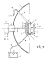
- a Cassegrain antenna according to the invention is shown in Figure 1.
- concave main reflector 1 of generally parabolic shape (paraboloid of revolution) and a convex auxiliary reflector 2 of generally hyperbolic shape (hyperboloid of revolution) of dimension much smaller than the main reflector 1 (for example a diameter approximately ten times smaller).
- a multimode excitation source 3 is placed at the top of the main reflector 1 and emits microwave waves towards the auxiliary reflector 2, which is kept centered in front of the source and coaxially with the main reflector by four rigid rods 4 of small diameter arranged in planes at 45 ° of the axis of the reflectors.
- Microwave power supply circuits designated by the reference 5 are placed behind the source 3, behind the main reflector 1.
- the controlled polarizer, 7, which comprises for example three sets 8, 9, 10, of double arrays of wire-diodes: each set comprises both a layer of wires- parallel diodes oriented generally in a given direction and a layer of diode wires oriented perpendicular to those of the other layer.
- control circuits 12 are placed making it possible to supply the diodes of the various networks directly or in reverse, and control circuits 13 making it possible to check and know the state of good or bad operation diodes (breaks or short circuits), therefore that of the polarization assembly.
- circuits are connected to the son-diodes by conductors 14, 15 passing through holes 17 of small diameter drilled near the edge of the reflector 2.
- the circuits 12 and 13 are placed in a sealed box 16 whose dimensions are such that it does not disturb the radiation of the antenna when it is placed behind the auxiliary reflector 2.
- the supply voltages of the diodes, the control orders, the control signals are conveyed by cables 18, 19 passing inside the tie rods 4 and coming from a control unit 11.
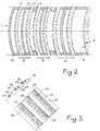
- FIG. 2 shows the detail of embodiment of the electronically controlled polarizer placed in front of the auxiliary reflector 2.
- hyperbolic as the surface 6 of the auxiliary reflector 2.
- the spacing of the panels, the thickness of each of them influence the polarization undergone by the microwave wave.
- the assemblies 8, 9 and 10 are all made in the same way, that is to say each with three panels such as 21, 22, 23 and they are separated by spacers 24.
- FIG. 3 represents a detail of embodiment of a panel 21 or 23, in cross section and in top view.
- the curved panel is made of a dielectric material and is provided with parallel grooves 25 for the wire-diodes, these grooves being wide enough to contain the diodes 26 connected by sections of wire 27.
- the wire-diodes, thus formed and maintained in the grooves 25 follow the curved shape of the panels 21 and 23.
- the diode wires which are parallel to each other can be separated by a distance of the order of half the wavelength of the radiation emitted, while the spacing between a diode wire and its supply wire would be of the order of tenth of the wavelength.
- the panels can be produced by molding directly giving the desired curved shape with the parallel grooves. The son-diodes are then put in place, after which the panels are assembled together, for example by strapping and fixed on the auxiliary reflector.
- the Cassegrain antenna which has just been described can be used in particular in tracking and ecartometry radar systems, trajectography, spatial listening, etc.
Landscapes
- Aerials With Secondary Devices (AREA)
Claims (3)
Applications Claiming Priority (2)
| Application Number | Priority Date | Filing Date | Title |
|---|---|---|---|
| FR8203422 | 1982-03-02 | ||
| FR8203422A FR2522888A1 (fr) | 1982-03-02 | 1982-03-02 | Antenne a double reflecteur a transformateur de polarisation incorpore |
Publications (2)
| Publication Number | Publication Date |
|---|---|
| EP0088681A1 EP0088681A1 (de) | 1983-09-14 |
| EP0088681B1 true EP0088681B1 (de) | 1988-03-02 |
Family
ID=9271489
Family Applications (1)
| Application Number | Title | Priority Date | Filing Date |
|---|---|---|---|
| EP19830400424 Expired EP0088681B1 (de) | 1982-03-02 | 1983-03-02 | Doppelreflektorantenne mit eingebautem Polarisationswandler |
Country Status (3)
| Country | Link |
|---|---|
| EP (1) | EP0088681B1 (de) |
| DE (1) | DE3375866D1 (de) |
| FR (1) | FR2522888A1 (de) |
Families Citing this family (2)
| Publication number | Priority date | Publication date | Assignee | Title |
|---|---|---|---|---|
| EP0381037A1 (de) * | 1989-01-31 | 1990-08-08 | Siemens-Albis Aktiengesellschaft | Antennensystem |
| GB0707147D0 (en) | 2007-04-13 | 2007-05-23 | Basic Device Ltd | Radiators |
Family Cites Families (5)
| Publication number | Priority date | Publication date | Assignee | Title |
|---|---|---|---|---|
| US3235870A (en) * | 1961-03-09 | 1966-02-15 | Hazeltine Research Inc | Double-reflector antenna with polarization-changing subreflector |
| GB1305117A (de) * | 1970-07-13 | 1973-01-31 | ||
| US3896440A (en) * | 1971-11-26 | 1975-07-22 | Westinghouse Electric Corp | Retrodirective passive beacon for simulating a moving target |
| DK143827C (da) * | 1973-05-23 | 1982-03-08 | Harris Corp | Passivt antenneelement |
| FR2382109A1 (fr) * | 1977-02-25 | 1978-09-22 | Thomson Csf | Transformateur de polarisation hyperfrequence |
-
1982
- 1982-03-02 FR FR8203422A patent/FR2522888A1/fr active Granted
-
1983
- 1983-03-02 EP EP19830400424 patent/EP0088681B1/de not_active Expired
- 1983-03-02 DE DE8383400424T patent/DE3375866D1/de not_active Expired
Also Published As
| Publication number | Publication date |
|---|---|
| FR2522888A1 (fr) | 1983-09-09 |
| DE3375866D1 (en) | 1988-04-07 |
| FR2522888B1 (de) | 1984-04-20 |
| EP0088681A1 (de) | 1983-09-14 |
Similar Documents
| Publication | Publication Date | Title |
|---|---|---|
| EP0205212B1 (de) | Modulare Mikrowellenantenneneinheiten und Antenne mit solchen Einheiten | |
| EP1416586B1 (de) | Antenne mit einer Filtermaterialanordnung | |
| EP1407512B1 (de) | Antenne | |
| CA2019181A1 (fr) | Element rayonnant diplexant | |
| CA2148796C (fr) | Antenne fil-plaque monopolaire | |
| EP0457880B1 (de) | Iff-bordantenne mit schaltbaren strahlungsdiagrammen | |
| EP1568104B1 (de) | Mehrfachstrahlantenne mit photonischem bandlückenmaterial | |
| EP1702388A1 (de) | Konfigurierbare und orientierbare antenne und entsprechende basisstation | |
| EP0886889A1 (de) | Breitbandige gedruckte gruppenantenne | |
| EP0899814A1 (de) | Strahlende Struktur | |
| FR2907602A1 (fr) | Antenne a fils multiples a double polarisation. | |
| EP3011639A1 (de) | Quelle für eine parabolantenne | |
| CA2460820C (fr) | Antenne a large bande ou multi-bandes | |
| EP1554777B1 (de) | Mehrfachstrahlantenne mit photonischem bandlückenmaterial | |
| EP1551078A1 (de) | Rundstrahler mit schwenkbarem Richtdiagramm | |
| EP0088681B1 (de) | Doppelreflektorantenne mit eingebautem Polarisationswandler | |
| FR2518828A1 (fr) | Filtre spatial de frequences et antenne comportant un tel filtre | |
| CA2808511C (fr) | Antenne plane pour terminal fonctionnant en double polarisation circulaire, terminal aeroporte et systeme de telecommunication par satellite comportant au moins une telle antenne | |
| FR2552273A1 (fr) | Antenne hyperfrequence omnidirectionnelle | |
| FR2854737A1 (fr) | Antenne a materiau bip multi-faisceaux et/ou multi- frequences et systeme mettant en oeuvre ces antennes. | |
| WO1991018428A1 (fr) | Antenne orientable plane, fonctionnant en micro-ondes | |
| WO2007074307A1 (fr) | Reflecteur bipolarisation configurable | |
| FR3076088A1 (fr) | Formateur de faisceaux quasi-optique, antenne elementaire, systeme antennaire, plateforme et procede de telecommunications associes | |
| EP0156684A1 (de) | Strahlendes Mirkowellenelement und seine Anwendung in einer elektronisch gesteuerten Antenne | |
| WO2015189136A1 (fr) | Antenne plate de telecommunication par satellite |
Legal Events
| Date | Code | Title | Description |
|---|---|---|---|
| PUAI | Public reference made under article 153(3) epc to a published international application that has entered the european phase |
Free format text: ORIGINAL CODE: 0009012 |
|
| AK | Designated contracting states |
Designated state(s): DE GB IT NL |
|
| 17P | Request for examination filed |
Effective date: 19831224 |
|
| 17Q | First examination report despatched |
Effective date: 19860204 |
|
| GRAA | (expected) grant |
Free format text: ORIGINAL CODE: 0009210 |
|
| AK | Designated contracting states |
Kind code of ref document: B1 Designated state(s): DE GB IT NL |
|
| ITF | It: translation for a ep patent filed | ||
| REF | Corresponds to: |
Ref document number: 3375866 Country of ref document: DE Date of ref document: 19880407 |
|
| GBT | Gb: translation of ep patent filed (gb section 77(6)(a)/1977) | ||
| PLBE | No opposition filed within time limit |
Free format text: ORIGINAL CODE: 0009261 |
|
| STAA | Information on the status of an ep patent application or granted ep patent |
Free format text: STATUS: NO OPPOSITION FILED WITHIN TIME LIMIT |
|
| 26N | No opposition filed | ||
| PGFP | Annual fee paid to national office [announced via postgrant information from national office to epo] |
Ref country code: NL Payment date: 19900331 Year of fee payment: 8 |
|
| PG25 | Lapsed in a contracting state [announced via postgrant information from national office to epo] |
Ref country code: NL Effective date: 19911001 |
|
| NLV4 | Nl: lapsed or anulled due to non-payment of the annual fee | ||
| ITTA | It: last paid annual fee | ||
| PGFP | Annual fee paid to national office [announced via postgrant information from national office to epo] |
Ref country code: DE Payment date: 20010214 Year of fee payment: 19 |
|
| PGFP | Annual fee paid to national office [announced via postgrant information from national office to epo] |
Ref country code: GB Payment date: 20010222 Year of fee payment: 19 |
|
| REG | Reference to a national code |
Ref country code: GB Ref legal event code: IF02 |
|
| PG25 | Lapsed in a contracting state [announced via postgrant information from national office to epo] |
Ref country code: GB Free format text: LAPSE BECAUSE OF NON-PAYMENT OF DUE FEES Effective date: 20020302 |
|
| PG25 | Lapsed in a contracting state [announced via postgrant information from national office to epo] |
Ref country code: DE Free format text: LAPSE BECAUSE OF NON-PAYMENT OF DUE FEES Effective date: 20021001 |
|
| GBPC | Gb: european patent ceased through non-payment of renewal fee |
Effective date: 20020302 |