EP0082993A2 - Verfahren zur selektiven Herstellung durch Ätzen von Öffnungen in einem Material mit variabler Dicke - Google Patents
Verfahren zur selektiven Herstellung durch Ätzen von Öffnungen in einem Material mit variabler Dicke Download PDFInfo
- Publication number
- EP0082993A2 EP0082993A2 EP82111306A EP82111306A EP0082993A2 EP 0082993 A2 EP0082993 A2 EP 0082993A2 EP 82111306 A EP82111306 A EP 82111306A EP 82111306 A EP82111306 A EP 82111306A EP 0082993 A2 EP0082993 A2 EP 0082993A2
- Authority
- EP
- European Patent Office
- Prior art keywords
- etching
- intensity
- curve
- end point
- etch
- Prior art date
- Legal status (The legal status is an assumption and is not a legal conclusion. Google has not performed a legal analysis and makes no representation as to the accuracy of the status listed.)
- Granted
Links
Images

Classifications
-
- C—CHEMISTRY; METALLURGY
- C23—COATING METALLIC MATERIAL; COATING MATERIAL WITH METALLIC MATERIAL; CHEMICAL SURFACE TREATMENT; DIFFUSION TREATMENT OF METALLIC MATERIAL; COATING BY VACUUM EVAPORATION, BY SPUTTERING, BY ION IMPLANTATION OR BY CHEMICAL VAPOUR DEPOSITION, IN GENERAL; INHIBITING CORROSION OF METALLIC MATERIAL OR INCRUSTATION IN GENERAL
- C23F—NON-MECHANICAL REMOVAL OF METALLIC MATERIAL FROM SURFACE; INHIBITING CORROSION OF METALLIC MATERIAL OR INCRUSTATION IN GENERAL; MULTI-STEP PROCESSES FOR SURFACE TREATMENT OF METALLIC MATERIAL INVOLVING AT LEAST ONE PROCESS PROVIDED FOR IN CLASS C23 AND AT LEAST ONE PROCESS COVERED BY SUBCLASS C21D OR C22F OR CLASS C25
- C23F4/00—Processes for removing metallic material from surfaces, not provided for in group C23F1/00 or C23F3/00
-
- H10P50/268—
-
- H10P50/283—
-
- H10P50/71—
-
- H10P50/73—
Definitions
- the invention relates to a method of selectively etching at least one opening in a given material on a substrate or layer of a different material wherein said given material has a variable thickness at the locations to be etched, and wherein a mask is provided overlying said given material, said mask defining the at least one opening at the locations to be etched.
- etching openings through certain material in such a way as to accurately control the opening size and also accurately control the edge profiles and undercutting of the etched openings.
- the openings are etched through a mask and the edge contour should terminate at the substrate in vertical alignment with the edge of the mask.
- This is etching polysilicon on an Si0 2 base in the manufacture of semiconductor chips.
- the etch takes place laterally as well as vertically leaving an opening which has curved side walls. It is desirable that the etch terminate as soon as the material has been etched through to the substrate so that the edge of the bottom part of the wall is exactly in vertical alignment with the opening in the mask. This is no particular problem if the material is of uniform thickness such that the etching at all locations is completed at the same time. However, there is normally significant variations in the thickness of the material being etched. Therefore, if the etch is continued to completion at the thickest part, there will be significant detrimental undercutting or etch bias of the thinner parts where the vertical etching terminates sooner, but the horizontal etching continues. Using anisotropic etching to eliminate any undercutting will not solve the problem since the walls will turn out vertical rather than with the desired curvature.
- the initial end point of removing the given material at the said location thereof to first expose the substrate is detected by monitoring the emission band, or peak, of a reactive species involved in said etching and terminating the etching at a particular location on the plot of the intensity of said band, or peak.
- a second derivative of the plot of said curve is used to determine and timely recognize said initial end point.
- an improved method is provided to etch openings in a material wherein the openings require precisely controlled size and side contours.
- This technique finds particular application in the processing of silicon wafers for integrated circuit chips, and the invention will be described for this particular application. It is to be understood, however, that it has such wider application, and can be used wherever such close tolerances of size as well as contour must be achieved in etching patterns.
- the invention will also be described in an embodiment of etching polysilicon on a substrate of Si0 2 . However, it can be used on any material that can be selectively etched through a mask.
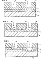
- a section through a particular silicon wafer during a step in the processing is shown.
- the silicon wafer designated by the reference character 10
- SiO 2 silicon dioxide
- a layer of polysilicon 14 which is to be etched in a given pattern.
- a mask of photoresist 16 which has been exposed and developed to define a pattern corresponding to the pattern to be etched in the polysilicon 14.
- Two of the openings of the pattern are shown and designated by the reference characters 18 and 20. Normally there are a great number of openings on each wafer but only two are shown for illustration.
- each of the layers, and especially the polysilicon layer 14 be as uniform as possible.
- precise thickness control cannot be obtained, and this variation in thickness is depicted in Figs. 1-3 by showing the polysilicon layer as being significantly thinner at the opening 18 than it is at opening 20. It is also possible that even at a given opening the thickness may vary from one side to the other. It is this variation in thickness of the polysilicon that makes it difficult to uniformly etch completely through the polysilicon at each opening and still maintain proper size and side contour control. This is because when the etching has been completed at one opening, i. e., 18, it is not completed at another opening, i. e., 20. If the etching continues, then the polysilicon at opening 18 will be over etched resulting in lateral undercutting and change in wall contour.
- the two step process of this invention assures a complete etch at all locations without any significant etch bias or over etch resulting in undercutting with resultant loss of shape and dimension at the thinner locations of the material.
- a first plasma etch step which is isotropic in character is performed on the polysilicon 14.
- This can be done in radial flow parallel plate reactor such as a Model PK 24 manufactured by Plasma Therm Corporation of Kresson, New Jersey.
- the reactor can be operated with a mixture of CF 4 and 0 2 gas with the upper plate powered to operate in a plasma etch mode. This will result in the performance of isotropic etching and will result in the polysilicon being removed.
- the pattern of removal of the polysilicon is shown in Fig. 2.
- the polysilicon 14 is removed both directly under the openings 18 and 20 and curved sides 22 are formed under the photoresist. This is the result of the isotropic character of the etch.
- the exact contour of the sides and the etch rate is a function of the power, gas mixture, gas pressure and temperature all of which can be varied and regulated to control these characteristics as is well known in the art.
- This first step of isotropically etching is continued until all of the polysilicon is removed from a first region, which is shown at the opening 18. Expressed another way, the isotropic etching continues until it first breaks through the polysilicon and exposes the silicon dioxide below at some opening.
- the curved sides 22 terminate at a point directly below the edge of the photoresist 16 forming the opening 18.
- This same curved configuration of the sides 22 is also present at the opening 20, with the curve terminating directly below the edge of the photoresist defining the opening 20.
- the polysilicon has not been completely removed, there still being an apprecible thickness left on the SiO 2 within the opening 20.
- the isotropic etching is discontinued.
- anisotropic etching is commenced. Anisotropic etching will etch only the polysilicon directly in line with the openings 18 or 20 and will not etch laterally.
- One technique for anisotropic etching employs the same device used for isotropic etching but varies the etching medium.
- One medium that can be used is C2F5Cl and 0 2 mixed. This can also be done as plasma etching powering only the upper electrode.
- the work pieces can be left in the same tool and only the atmosphere charged, and then anisotropic etching can be performed with the selection of the desired power, gas pressure, gas mixture and temperature as is known in the art.
- the anisotropic etching continues until all of the remaining polysilicon in all of the openings is removed. This condition is represented in Fig. 3 by the solid lines. As can be seen in Fig. 3, the curvature of sides of the polysilicon in the opening 20 has been changed slightly at the lower end as shown at 24, but this slight change is perfectly acceptable. The anisotropic etch will not have any effect on the polysilicon adjacent the opening 18 since it does not etch laterally nor does it etch the Si0 2 underlayer; hence, there will be no undercutting as would have occurred with continuation of isotropic etching.
- the first or initial end point i. e., when the initial etch has first broken through the polysilicon and exposed the substrate and also when the second end point occurs, i. e., when all of the polysilicon exposed at all the openings is removed. It is necessary that these determinations be made irrespective of the total volume of product being processed, i. e., that various configured wafers and various numbers of wafers can be processed with the same accuracy of control. It is also necessary that the first and second end point be clearly determined for automatic control of any apparatus, and this is especially critical for the first end point detection which must be quickly and accurately recognized as it occurs to prevent etch bias or undercutting from occurring.
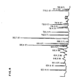
- Fig. 4 a representation of the emission spectrum of a mixture of CF 4 and 0 2 plasma between 610 and 780 nanometers is shown.
- this spectrum various fluorine, oxygen, and nitrogen peaks are indicated. It has been observed that during etching the intensity of some of these peaks will vary in intensity, and some will not. With those peaks that do vary, the intensity stays relatively constant as long as the SiO 2 substrate is completely covered with polysilicon. As soon as the etch first breaks through polysilicon to expose the Si0 2 the intensity starts to change and this change continues until the polysilicon has been completely removed, at which time the intensity stablizes.
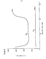
- a plot of two of the peaks shown in Fig. 4, i. e., the 703.7 fluorine peak and 696.6 fluorine peak is shown in F ig. 5, designated as lines 30 and 32, respectively, wherein the intensity is plotted on the Y axis and etch time on the X axis.
- the 703.7 peak starts out at a given level and as etching starts drops to a level of about half the initial value. This lower level continues for a period of time after which the curve starts to rise and then levels off at about the initial value.
- the intensity of 696.6 fluorine peak remains essentially constant both during the earlier etch period and thereafter. Hence, this peak is non-sensitive to the reaction. Thus, it would be good if the point at which the 703.7 peak makes a definite change upward could be reliably and accurately detected and used to control the termination of the isotropic etch. However, merely monitoring this curve does not provide the prerequiste precision and reliability for determing this initial end point for several reasons. First, while the intensity may be relatively constant during the etching cycle before the start of the change, the actual intensity of this may vary from sample to sample. Also, while the curve is relatively flat there still are variations of the readings and the processing of the signal to remove these variations cannot accurately be accomplished to provide an early enough awareness that this first or initial end point has been reached.
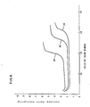
- curves can be generated by utilizing the ratio of certain peak intensities, for example, the ratio of the 703.7 peak intensity to the 696.6 peak intensity. Since the 703.7 peak intensity changes when the first end point is being reached and continues to change until the second end point, and the 696.6 peak intensity remains constant, a plot of one divided by the other will remove any variations that are constant to the system as a whole. Three such curves are shown in Fig. 6. One curve 34 is plotted for 11 wafers as a batch, one curve 36 for 9 wafers, and one curve 38 for 7 wafers. While this removes the system variations and also provides a more precise shape of the curves, it still is sensitive to the amount of material being etched in the lot, and, hence, a specific intensity level would not be a proper indication in all cases.
- the ratio of certain peak intensities for example, the ratio of the 703.7 peak intensity to the 696.6 peak intensity. Since the 703.7 peak intensity changes when the first end point is being reached and continues to change until the second end point, and the 696.6
- Another way of plotting the curve of the changing intensity is by sampling the intensity of the band which changes at designated intervals and dividing each sensed value by the immediately previously sensed value.
- Such a plot of curves 40, 42, and 44 of the 703.7 band intensity for wafer lot sizes of eight, six and four wafers, respectively, is shown in Fig.7. While this removes the error due to size of the lot or volume of material being etched, it still shows a wide variant of the change in intensity with various lot sizes and volumns of material being etched.
- a plot of the second derivative of wafer curve 40 of Fig. 7 is shown in Fig. 8 as curve 46.
- the point labeled A in Fig. 8 corresponds to the point A on the eight wafer curve 40 in Fig. 7.
- the point A of the curve in Fig. 8 is a very sharp peak. As can be seen in Fig. 8, this point A is represented by a very abrupt change from a very positive slope to a very negative slope in the curve. (This is actually a change in direction of the first derivative of this curve.) This is a readily observable point, clearly defined and can easily be recognized by either a machine or an operator; and it is easy to utilize as a machine or operator recognizable point to terminate the isotropic etching. Also, this point expressed as a second derivative can be easily recognized as it occurs and is not dependent upon the rest of the curve to be traced to be recognizable. Also, it will be apparent that point A on the curve in Fig.
- the first or isotropic etch process is stopped, which operation preferably is performed responsive to a signal generated by the monitoring device when the peak A is sensed and the slope changes from positive to negative.
- One very suitable device for monitoring the intensity, plotting the curves, performing the second derivative calculation and initiating the stop process signal is an optical multichannel analyzer, such as the OMA 2 manufactured by Princeton Applied Research Co., Princeton, New Jersey.
- the etch process is completed, as indicated above, by anisotropic etching.
- the second or final end point of this opearation is not particularly critical, since over etching or damage to the substrate cannot occur during the anisotropic etch, and similar techniques of measuring optical emission can be used to determine this final end point as is well known in the art.
Landscapes
- Chemical & Material Sciences (AREA)
- Engineering & Computer Science (AREA)
- Materials Engineering (AREA)
- Mechanical Engineering (AREA)
- Metallurgy (AREA)
- Organic Chemistry (AREA)
- Drying Of Semiconductors (AREA)
- ing And Chemical Polishing (AREA)
Applications Claiming Priority (2)
| Application Number | Priority Date | Filing Date | Title |
|---|---|---|---|
| US334181 | 1981-12-24 | ||
| US06/334,181 US4457820A (en) | 1981-12-24 | 1981-12-24 | Two step plasma etching |
Publications (3)
| Publication Number | Publication Date |
|---|---|
| EP0082993A2 true EP0082993A2 (de) | 1983-07-06 |
| EP0082993A3 EP0082993A3 (en) | 1986-10-29 |
| EP0082993B1 EP0082993B1 (de) | 1989-08-23 |
Family
ID=23305975
Family Applications (1)
| Application Number | Title | Priority Date | Filing Date |
|---|---|---|---|
| EP82111306A Expired EP0082993B1 (de) | 1981-12-24 | 1982-12-07 | Verfahren zur selektiven Herstellung durch Ätzen von Öffnungen in einem Material mit variabler Dicke |
Country Status (5)
| Country | Link |
|---|---|
| US (1) | US4457820A (de) |
| EP (1) | EP0082993B1 (de) |
| JP (1) | JPS58110678A (de) |
| CA (1) | CA1191479A (de) |
| DE (1) | DE3279909D1 (de) |
Cited By (6)
| Publication number | Priority date | Publication date | Assignee | Title |
|---|---|---|---|---|
| FR2587838A1 (fr) * | 1985-09-20 | 1987-03-27 | Radiotechnique Compelec | Procede pour aplanir la surface d'un dispositif semi-conducteur utilisant du nitrure de silicium comme materiau isolant |
| FR2599892A1 (fr) * | 1986-06-10 | 1987-12-11 | Schiltz Andre | Procede d'aplanissement d'un substrat semiconducteur revetu d'une couche dielectrique |
| EP0212251A3 (en) * | 1985-08-09 | 1988-03-16 | International Business Machines Corporation | Process using dry etchant to avoid mask-and-etch cycle |
| EP0198507A3 (de) * | 1985-04-19 | 1988-12-14 | Matsushita Electronics Corporation | Verfahren zur Endpunktbestimmung beim Ätzen |
| EP0529717A3 (en) * | 1991-08-23 | 1993-09-22 | N.V. Philips' Gloeilampenfabrieken | Method of manufacturing a semiconductor device having overlapping contacts |
| WO1996021243A1 (en) * | 1995-01-03 | 1996-07-11 | Advanced Micro Devices, Inc. | Method of etching conductive lines without undercutting |
Families Citing this family (49)
| Publication number | Priority date | Publication date | Assignee | Title |
|---|---|---|---|---|
| US4617193A (en) * | 1983-06-16 | 1986-10-14 | Digital Equipment Corporation | Planar interconnect for integrated circuits |
| US4634645A (en) * | 1984-04-13 | 1987-01-06 | Nippon Telegraph And Telephone Corporation | Method of forming resist micropattern |
| US4566935A (en) * | 1984-07-31 | 1986-01-28 | Texas Instruments Incorporated | Spatial light modulator and method |
| FR2598256B1 (fr) * | 1986-04-30 | 1988-07-08 | Thomson Csf | Procede de gravure seche selective de couches de materiaux semi-conducteurs iii-v, et transistor obtenu par ce procede. |
| US4936967A (en) * | 1987-01-05 | 1990-06-26 | Hitachi, Ltd. | Method of detecting an end point of plasma treatment |
| US4800170A (en) * | 1987-10-02 | 1989-01-24 | General Motors Corporation | Process for forming in a silicon oxide layer a portion with vertical side walls |
| GB2214870B (en) * | 1988-02-20 | 1991-09-11 | Stc Plc | Plasma etching process |
| JPH01226153A (ja) * | 1988-03-07 | 1989-09-08 | Hitachi Ltd | エッチング終点判定装置 |
| JPH01235336A (ja) * | 1988-03-16 | 1989-09-20 | Hitachi Ltd | エッチング終点判定装置 |
| JP2821132B2 (ja) * | 1988-03-23 | 1998-11-05 | 株式会社日立製作所 | エッチング終点判定方法 |
| JP2692199B2 (ja) * | 1988-11-19 | 1997-12-17 | 富士通株式会社 | エッチング終点検出装置 |
| DE3915650A1 (de) * | 1989-05-12 | 1990-11-15 | Siemens Ag | Verfahren zur strukturierung einer auf einem halbleiterschichtaufbau angeordneten schicht |
| US5118378A (en) * | 1989-10-10 | 1992-06-02 | Hitachi, Ltd. | Apparatus for detecting an end point of etching |
| US5118382A (en) * | 1990-08-10 | 1992-06-02 | Ibm Corporation | Elimination of etch stop undercut |
| US5362356A (en) * | 1990-12-20 | 1994-11-08 | Lsi Logic Corporation | Plasma etching process control |
| US5877032A (en) * | 1995-10-12 | 1999-03-02 | Lucent Technologies Inc. | Process for device fabrication in which the plasma etch is controlled by monitoring optical emission |
| US5425839A (en) * | 1992-05-14 | 1995-06-20 | Texas Instruments Incorporated | Method for rapidly etching material on a semiconductor device |
| US5372673A (en) * | 1993-01-25 | 1994-12-13 | Motorola, Inc. | Method for processing a layer of material while using insitu monitoring and control |
| US5348614A (en) * | 1993-06-22 | 1994-09-20 | Lsi Logic Corporation | Process for dynamic control of the concentration of one or more reactants in a plasma-enhanced process for formation of integrated circuit structures |
| US5591300A (en) * | 1995-06-07 | 1997-01-07 | Vtc Inc. | Single crystal silicon dry-etch endpoint based on dopant-dependent and thermally-assisted etch rates |
| JP3766991B2 (ja) * | 1995-10-20 | 2006-04-19 | 株式会社日立製作所 | プラズマ処理の終点検出方法及び装置、並びに本検出方法及び装置を用いた半導体製造方法及び装置 |
| US5788869A (en) * | 1995-11-02 | 1998-08-04 | Digital Equipment Corporation | Methodology for in situ etch stop detection and control of plasma etching process and device design to minimize process chamber contamination |
| FR2757941B1 (fr) * | 1996-12-30 | 1999-01-22 | Commissariat Energie Atomique | Procede de realisation d'un element suspendu dans une structure micro-usinee |
| US6165312A (en) * | 1998-04-23 | 2000-12-26 | Sandia Corporation | Method and apparatus for monitoring plasma processing operations |
| DE10004391C2 (de) * | 2000-02-02 | 2002-05-16 | Infineon Technologies Ag | Verfahren zur Durchführung eines Plasmaätzprozesses |
| US6461877B1 (en) * | 2000-06-30 | 2002-10-08 | International Business Machines Corporation | Variable data compensation for vias or contacts |
| US7480983B2 (en) * | 2004-05-28 | 2009-01-27 | Hitachi Global Storage Technologies Netherlands B.V. | Method for making magnetic write head |
| US8501631B2 (en) | 2009-11-19 | 2013-08-06 | Lam Research Corporation | Plasma processing system control based on RF voltage |
| US10157729B2 (en) | 2012-02-22 | 2018-12-18 | Lam Research Corporation | Soft pulsing |
| US9368329B2 (en) | 2012-02-22 | 2016-06-14 | Lam Research Corporation | Methods and apparatus for synchronizing RF pulses in a plasma processing system |
| US9114666B2 (en) | 2012-02-22 | 2015-08-25 | Lam Research Corporation | Methods and apparatus for controlling plasma in a plasma processing system |
| US10128090B2 (en) | 2012-02-22 | 2018-11-13 | Lam Research Corporation | RF impedance model based fault detection |
| US9295148B2 (en) | 2012-12-14 | 2016-03-22 | Lam Research Corporation | Computation of statistics for statistical data decimation |
| US9320126B2 (en) | 2012-12-17 | 2016-04-19 | Lam Research Corporation | Determining a value of a variable on an RF transmission model |
| US9171699B2 (en) | 2012-02-22 | 2015-10-27 | Lam Research Corporation | Impedance-based adjustment of power and frequency |
| US9462672B2 (en) | 2012-02-22 | 2016-10-04 | Lam Research Corporation | Adjustment of power and frequency based on three or more states |
| US10325759B2 (en) | 2012-02-22 | 2019-06-18 | Lam Research Corporation | Multiple control modes |
| US9197196B2 (en) | 2012-02-22 | 2015-11-24 | Lam Research Corporation | State-based adjustment of power and frequency |
| US9390893B2 (en) | 2012-02-22 | 2016-07-12 | Lam Research Corporation | Sub-pulsing during a state |
| US9842725B2 (en) | 2013-01-31 | 2017-12-12 | Lam Research Corporation | Using modeling to determine ion energy associated with a plasma system |
| US9502216B2 (en) | 2013-01-31 | 2016-11-22 | Lam Research Corporation | Using modeling to determine wafer bias associated with a plasma system |
| US9155182B2 (en) | 2013-01-11 | 2015-10-06 | Lam Research Corporation | Tuning a parameter associated with plasma impedance |
| JP2014150149A (ja) * | 2013-01-31 | 2014-08-21 | Ulvac Japan Ltd | エッチング方法及びエッチング装置 |
| US9620337B2 (en) | 2013-01-31 | 2017-04-11 | Lam Research Corporation | Determining a malfunctioning device in a plasma system |
| US9779196B2 (en) | 2013-01-31 | 2017-10-03 | Lam Research Corporation | Segmenting a model within a plasma system |
| US9502221B2 (en) | 2013-07-26 | 2016-11-22 | Lam Research Corporation | Etch rate modeling and use thereof with multiple parameters for in-chamber and chamber-to-chamber matching |
| US9594105B2 (en) | 2014-01-10 | 2017-03-14 | Lam Research Corporation | Cable power loss determination for virtual metrology |
| US10950421B2 (en) | 2014-04-21 | 2021-03-16 | Lam Research Corporation | Using modeling for identifying a location of a fault in an RF transmission system for a plasma system |
| US9536749B2 (en) | 2014-12-15 | 2017-01-03 | Lam Research Corporation | Ion energy control by RF pulse shape |
Family Cites Families (6)
| Publication number | Priority date | Publication date | Assignee | Title |
|---|---|---|---|---|
| DE2626420C3 (de) * | 1976-06-12 | 1979-11-29 | Ibm Deutschland Gmbh, 7000 Stuttgart | Verfahren zum gleichzeitigen Ätzen von mehreren durchgehenden Löchern |
| US4182646A (en) * | 1978-07-27 | 1980-01-08 | John Zajac | Process of etching with plasma etch gas |
| US4289574A (en) * | 1979-04-30 | 1981-09-15 | Fairchild Camera & Instrument Corp. | Process for patterning metal connections on a semiconductor structure by using an aluminum oxide etch resistant layer |
| JPS55157233A (en) * | 1979-05-28 | 1980-12-06 | Hitachi Ltd | Method and apparatus for monitoring etching |
| JPS5690525A (en) * | 1979-11-28 | 1981-07-22 | Fujitsu Ltd | Manufacture of semiconductor device |
| US4380488A (en) * | 1980-10-14 | 1983-04-19 | Branson International Plasma Corporation | Process and gas mixture for etching aluminum |
-
1981
- 1981-12-24 US US06/334,181 patent/US4457820A/en not_active Expired - Lifetime
-
1982
- 1982-10-08 JP JP57176498A patent/JPS58110678A/ja active Granted
- 1982-11-17 CA CA000415730A patent/CA1191479A/en not_active Expired
- 1982-12-07 EP EP82111306A patent/EP0082993B1/de not_active Expired
- 1982-12-07 DE DE8282111306T patent/DE3279909D1/de not_active Expired
Cited By (8)
| Publication number | Priority date | Publication date | Assignee | Title |
|---|---|---|---|---|
| EP0198507A3 (de) * | 1985-04-19 | 1988-12-14 | Matsushita Electronics Corporation | Verfahren zur Endpunktbestimmung beim Ätzen |
| EP0212251A3 (en) * | 1985-08-09 | 1988-03-16 | International Business Machines Corporation | Process using dry etchant to avoid mask-and-etch cycle |
| FR2587838A1 (fr) * | 1985-09-20 | 1987-03-27 | Radiotechnique Compelec | Procede pour aplanir la surface d'un dispositif semi-conducteur utilisant du nitrure de silicium comme materiau isolant |
| EP0216425A3 (en) * | 1985-09-20 | 1987-08-05 | Rtc-Compelec | Process for planarizing the surface of a semiconductor device using silicon nitride as an insulating material |
| FR2599892A1 (fr) * | 1986-06-10 | 1987-12-11 | Schiltz Andre | Procede d'aplanissement d'un substrat semiconducteur revetu d'une couche dielectrique |
| EP0529717A3 (en) * | 1991-08-23 | 1993-09-22 | N.V. Philips' Gloeilampenfabrieken | Method of manufacturing a semiconductor device having overlapping contacts |
| WO1996021243A1 (en) * | 1995-01-03 | 1996-07-11 | Advanced Micro Devices, Inc. | Method of etching conductive lines without undercutting |
| US5702564A (en) * | 1995-01-03 | 1997-12-30 | Advanced Micro Devices, Inc. | Method of etching conductive lines without undercutting |
Also Published As
| Publication number | Publication date |
|---|---|
| JPS6159396B2 (de) | 1986-12-16 |
| US4457820A (en) | 1984-07-03 |
| EP0082993B1 (de) | 1989-08-23 |
| CA1191479A (en) | 1985-08-06 |
| DE3279909D1 (en) | 1989-09-28 |
| EP0082993A3 (en) | 1986-10-29 |
| JPS58110678A (ja) | 1983-07-01 |
Similar Documents
| Publication | Publication Date | Title |
|---|---|---|
| EP0082993B1 (de) | Verfahren zur selektiven Herstellung durch Ätzen von Öffnungen in einem Material mit variabler Dicke | |
| EP0212219B1 (de) | Verfahren zur Sichtbarkeitsverbesserung von Ausrichtmarkierungen erster Ordnung | |
| US4263088A (en) | Method for process control of a plasma reaction | |
| US4717446A (en) | Method of detecting the endpoint of the etch of epitaxially grown silicon | |
| US4902377A (en) | Sloped contact etch process | |
| US4496425A (en) | Technique for determining the end point of an etching process | |
| KR100659163B1 (ko) | 플라즈마 에칭 공정의 정확도를 개선시키기 위한 방법 및장치 | |
| JPH0528895B2 (de) | ||
| US4357195A (en) | Apparatus for controlling a plasma reaction | |
| US4528438A (en) | End point control in plasma etching | |
| EP0536968A2 (de) | Verfahren zum Erzeugen von Kontaktlöchern in der Herstellung von Halbleiteranordnungen | |
| JPS6013072B2 (ja) | プラズマエツチングの終点制御方法および装置 | |
| EP0314522B1 (de) | Verfahren zum Ätzen von Gräben | |
| US5261998A (en) | Method for detecting an end point of etching in semiconductor manufacture using the emission spectrum of helium | |
| EP0840364A1 (de) | Verfahren zur Herstellung einer Halbleiteranordnung | |
| JPH08148474A (ja) | ドライエッチングの終点検出方法および装置 | |
| US4311546A (en) | Method of manufacturing semiconductor device | |
| JPH04370929A (ja) | ドライエッチング方法 | |
| US20030119215A1 (en) | Method and system for determining a performance of plasma etch equipment | |
| KR920010752B1 (ko) | 콤팩트 인-라인 에치 모니터링 패턴 측정 방법 | |
| KR100260243B1 (ko) | 압력센서 및 그 제조방법 | |
| JPH04309222A (ja) | 半導体装置 | |
| JPH0430518A (ja) | 半導体装置の製造方法 | |
| JPS61208833A (ja) | 半導体装置の製造方法 | |
| JP2559731B2 (ja) | 半導体装置の製造方法 |
Legal Events
| Date | Code | Title | Description |
|---|---|---|---|
| PUAI | Public reference made under article 153(3) epc to a published international application that has entered the european phase |
Free format text: ORIGINAL CODE: 0009012 |
|
| AK | Designated contracting states |
Designated state(s): DE FR GB IT |
|
| 17P | Request for examination filed |
Effective date: 19831021 |
|
| PUAL | Search report despatched |
Free format text: ORIGINAL CODE: 0009013 |
|
| AK | Designated contracting states |
Kind code of ref document: A3 Designated state(s): DE FR GB IT |
|
| 17Q | First examination report despatched |
Effective date: 19880316 |
|
| GRAA | (expected) grant |
Free format text: ORIGINAL CODE: 0009210 |
|
| AK | Designated contracting states |
Kind code of ref document: B1 Designated state(s): DE FR GB IT |
|
| REF | Corresponds to: |
Ref document number: 3279909 Country of ref document: DE Date of ref document: 19890928 |
|
| ITF | It: translation for a ep patent filed | ||
| ET | Fr: translation filed | ||
| PLBE | No opposition filed within time limit |
Free format text: ORIGINAL CODE: 0009261 |
|
| STAA | Information on the status of an ep patent application or granted ep patent |
Free format text: STATUS: NO OPPOSITION FILED WITHIN TIME LIMIT |
|
| 26N | No opposition filed | ||
| ITTA | It: last paid annual fee | ||
| PGFP | Annual fee paid to national office [announced via postgrant information from national office to epo] |
Ref country code: FR Payment date: 19921124 Year of fee payment: 11 |
|
| PGFP | Annual fee paid to national office [announced via postgrant information from national office to epo] |
Ref country code: GB Payment date: 19921126 Year of fee payment: 11 |
|
| PGFP | Annual fee paid to national office [announced via postgrant information from national office to epo] |
Ref country code: DE Payment date: 19921214 Year of fee payment: 11 |
|
| PG25 | Lapsed in a contracting state [announced via postgrant information from national office to epo] |
Ref country code: GB Effective date: 19931207 |
|
| GBPC | Gb: european patent ceased through non-payment of renewal fee |
Effective date: 19931207 |
|
| PG25 | Lapsed in a contracting state [announced via postgrant information from national office to epo] |
Ref country code: FR Effective date: 19940831 |
|
| PG25 | Lapsed in a contracting state [announced via postgrant information from national office to epo] |
Ref country code: DE Effective date: 19940901 |
|
| REG | Reference to a national code |
Ref country code: FR Ref legal event code: ST |