EP0078935B1 - Condensateur à film épais par la technique des circuits imprimés - Google Patents
Condensateur à film épais par la technique des circuits imprimés Download PDFInfo
- Publication number
- EP0078935B1 EP0078935B1 EP82109533A EP82109533A EP0078935B1 EP 0078935 B1 EP0078935 B1 EP 0078935B1 EP 82109533 A EP82109533 A EP 82109533A EP 82109533 A EP82109533 A EP 82109533A EP 0078935 B1 EP0078935 B1 EP 0078935B1
- Authority
- EP
- European Patent Office
- Prior art keywords
- capacitor
- dielectric
- printed
- dielectric layer
- screen
- Prior art date
- Legal status (The legal status is an assumption and is not a legal conclusion. Google has not performed a legal analysis and makes no representation as to the accuracy of the status listed.)
- Expired
Links
- 239000003990 capacitor Substances 0.000 title claims description 137
- 238000000034 method Methods 0.000 title claims description 38
- 239000004020 conductor Substances 0.000 claims description 59
- 238000001465 metallisation Methods 0.000 claims description 30
- 238000004519 manufacturing process Methods 0.000 claims description 19
- 239000000463 material Substances 0.000 claims description 18
- 239000000758 substrate Substances 0.000 claims description 18
- KDLHZDBZIXYQEI-UHFFFAOYSA-N Palladium Chemical compound [Pd] KDLHZDBZIXYQEI-UHFFFAOYSA-N 0.000 claims description 15
- 230000008569 process Effects 0.000 claims description 15
- 238000007650 screen-printing Methods 0.000 claims description 14
- 229910052751 metal Inorganic materials 0.000 claims description 12
- 239000002184 metal Substances 0.000 claims description 12
- 239000003054 catalyst Substances 0.000 claims description 11
- 239000000919 ceramic Substances 0.000 claims description 10
- 239000000126 substance Substances 0.000 claims description 10
- 239000006185 dispersion Substances 0.000 claims description 9
- 239000002861 polymer material Substances 0.000 claims description 9
- 239000002952 polymeric resin Substances 0.000 claims description 9
- 238000012545 processing Methods 0.000 claims description 9
- 229920003002 synthetic resin Polymers 0.000 claims description 9
- 239000011888 foil Substances 0.000 claims description 7
- 239000011159 matrix material Substances 0.000 claims description 7
- 230000004913 activation Effects 0.000 claims description 6
- 238000005530 etching Methods 0.000 claims description 6
- 239000011521 glass Substances 0.000 claims description 6
- 229920000877 Melamine resin Polymers 0.000 claims description 5
- 239000003822 epoxy resin Substances 0.000 claims description 4
- 229910052763 palladium Inorganic materials 0.000 claims description 4
- 229920000647 polyepoxide Polymers 0.000 claims description 4
- 229920005749 polyurethane resin Polymers 0.000 claims description 4
- 229920000642 polymer Polymers 0.000 claims description 2
- 229920005989 resin Polymers 0.000 claims description 2
- 239000011347 resin Substances 0.000 claims description 2
- 230000003213 activating effect Effects 0.000 claims 3
- 229920001225 polyester resin Polymers 0.000 claims 3
- 239000004645 polyester resin Substances 0.000 claims 3
- 229920002430 Fibre-reinforced plastic Polymers 0.000 claims 2
- 229920013632 Ryton Polymers 0.000 claims 2
- 239000004736 Ryton® Substances 0.000 claims 2
- 230000015572 biosynthetic process Effects 0.000 claims 2
- 150000001875 compounds Chemical class 0.000 claims 2
- 239000000470 constituent Substances 0.000 claims 2
- 239000011151 fibre-reinforced plastic Substances 0.000 claims 2
- 238000005253 cladding Methods 0.000 claims 1
- 239000004922 lacquer Substances 0.000 claims 1
- 238000005516 engineering process Methods 0.000 description 11
- PXHVJJICTQNCMI-UHFFFAOYSA-N Nickel Chemical compound [Ni] PXHVJJICTQNCMI-UHFFFAOYSA-N 0.000 description 10
- 229910052709 silver Inorganic materials 0.000 description 10
- BQCADISMDOOEFD-UHFFFAOYSA-N Silver Chemical compound [Ag] BQCADISMDOOEFD-UHFFFAOYSA-N 0.000 description 9
- 238000000576 coating method Methods 0.000 description 9
- 239000004332 silver Substances 0.000 description 9
- 238000007639 printing Methods 0.000 description 8
- 239000003989 dielectric material Substances 0.000 description 6
- 229910052759 nickel Inorganic materials 0.000 description 5
- RYGMFSIKBFXOCR-UHFFFAOYSA-N Copper Chemical compound [Cu] RYGMFSIKBFXOCR-UHFFFAOYSA-N 0.000 description 4
- 239000011230 binding agent Substances 0.000 description 4
- 229910052802 copper Inorganic materials 0.000 description 4
- 239000010949 copper Substances 0.000 description 4
- 238000013461 design Methods 0.000 description 4
- 239000000945 filler Substances 0.000 description 4
- 239000000203 mixture Substances 0.000 description 4
- 125000006850 spacer group Chemical group 0.000 description 4
- 239000012190 activator Substances 0.000 description 3
- 230000008901 benefit Effects 0.000 description 3
- 229910052737 gold Inorganic materials 0.000 description 3
- 239000010931 gold Substances 0.000 description 3
- 230000010354 integration Effects 0.000 description 3
- 229920000728 polyester Polymers 0.000 description 3
- 101100028920 Neurospora crassa (strain ATCC 24698 / 74-OR23-1A / CBS 708.71 / DSM 1257 / FGSC 987) cfp gene Proteins 0.000 description 2
- 239000004698 Polyethylene Substances 0.000 description 2
- 239000011195 cermet Substances 0.000 description 2
- 238000000151 deposition Methods 0.000 description 2
- 230000008021 deposition Effects 0.000 description 2
- 238000010586 diagram Methods 0.000 description 2
- PCHJSUWPFVWCPO-UHFFFAOYSA-N gold Chemical compound [Au] PCHJSUWPFVWCPO-UHFFFAOYSA-N 0.000 description 2
- 230000005012 migration Effects 0.000 description 2
- 238000013508 migration Methods 0.000 description 2
- 150000002941 palladium compounds Chemical class 0.000 description 2
- 239000000123 paper Substances 0.000 description 2
- 229920006267 polyester film Polymers 0.000 description 2
- -1 polyethylene Polymers 0.000 description 2
- 229920000573 polyethylene Polymers 0.000 description 2
- 229920001721 polyimide Polymers 0.000 description 2
- 239000004593 Epoxy Substances 0.000 description 1
- 239000001856 Ethyl cellulose Substances 0.000 description 1
- ZZSNKZQZMQGXPY-UHFFFAOYSA-N Ethyl cellulose Chemical compound CCOCC1OC(OC)C(OCC)C(OCC)C1OC1C(O)C(O)C(OC)C(CO)O1 ZZSNKZQZMQGXPY-UHFFFAOYSA-N 0.000 description 1
- 239000004642 Polyimide Substances 0.000 description 1
- 239000000853 adhesive Substances 0.000 description 1
- 230000001070 adhesive effect Effects 0.000 description 1
- WUOACPNHFRMFPN-UHFFFAOYSA-N alpha-terpineol Chemical compound CC1=CCC(C(C)(C)O)CC1 WUOACPNHFRMFPN-UHFFFAOYSA-N 0.000 description 1
- 239000012876 carrier material Substances 0.000 description 1
- 230000015556 catabolic process Effects 0.000 description 1
- 239000003638 chemical reducing agent Substances 0.000 description 1
- 239000011248 coating agent Substances 0.000 description 1
- 238000006731 degradation reaction Methods 0.000 description 1
- SQIFACVGCPWBQZ-UHFFFAOYSA-N delta-terpineol Natural products CC(C)(O)C1CCC(=C)CC1 SQIFACVGCPWBQZ-UHFFFAOYSA-N 0.000 description 1
- 230000000881 depressing effect Effects 0.000 description 1
- 238000010017 direct printing Methods 0.000 description 1
- 230000000694 effects Effects 0.000 description 1
- 238000007772 electroless plating Methods 0.000 description 1
- 229920001249 ethyl cellulose Polymers 0.000 description 1
- 235000019325 ethyl cellulose Nutrition 0.000 description 1
- 238000010348 incorporation Methods 0.000 description 1
- 238000009413 insulation Methods 0.000 description 1
- 238000003475 lamination Methods 0.000 description 1
- 239000002245 particle Substances 0.000 description 1
- 238000002161 passivation Methods 0.000 description 1
- 229920002120 photoresistant polymer Polymers 0.000 description 1
- 239000004033 plastic Substances 0.000 description 1
- 229920003023 plastic Polymers 0.000 description 1
- 229920002635 polyurethane Polymers 0.000 description 1
- 239000004814 polyurethane Substances 0.000 description 1
- 239000000843 powder Substances 0.000 description 1
- 238000003825 pressing Methods 0.000 description 1
- 230000001681 protective effect Effects 0.000 description 1
- 238000006722 reduction reaction Methods 0.000 description 1
- 239000010944 silver (metal) Substances 0.000 description 1
- 239000007921 spray Substances 0.000 description 1
- 229940116411 terpineol Drugs 0.000 description 1
- 239000002966 varnish Substances 0.000 description 1
Images

Classifications
-
- H—ELECTRICITY
- H05—ELECTRIC TECHNIQUES NOT OTHERWISE PROVIDED FOR
- H05K—PRINTED CIRCUITS; CASINGS OR CONSTRUCTIONAL DETAILS OF ELECTRIC APPARATUS; MANUFACTURE OF ASSEMBLAGES OF ELECTRICAL COMPONENTS
- H05K1/00—Printed circuits
- H05K1/16—Printed circuits incorporating printed electric components, e.g. printed resistor, capacitor, inductor
- H05K1/162—Printed circuits incorporating printed electric components, e.g. printed resistor, capacitor, inductor incorporating printed capacitors
-
- H—ELECTRICITY
- H01—ELECTRIC ELEMENTS
- H01G—CAPACITORS; CAPACITORS, RECTIFIERS, DETECTORS, SWITCHING DEVICES, LIGHT-SENSITIVE OR TEMPERATURE-SENSITIVE DEVICES OF THE ELECTROLYTIC TYPE
- H01G4/00—Fixed capacitors; Processes of their manufacture
- H01G4/002—Details
- H01G4/018—Dielectrics
- H01G4/20—Dielectrics using combinations of dielectrics from more than one of groups H01G4/02 - H01G4/06
-
- H—ELECTRICITY
- H01—ELECTRIC ELEMENTS
- H01G—CAPACITORS; CAPACITORS, RECTIFIERS, DETECTORS, SWITCHING DEVICES, LIGHT-SENSITIVE OR TEMPERATURE-SENSITIVE DEVICES OF THE ELECTROLYTIC TYPE
- H01G4/00—Fixed capacitors; Processes of their manufacture
- H01G4/38—Multiple capacitors, i.e. structural combinations of fixed capacitors
-
- H—ELECTRICITY
- H05—ELECTRIC TECHNIQUES NOT OTHERWISE PROVIDED FOR
- H05K—PRINTED CIRCUITS; CASINGS OR CONSTRUCTIONAL DETAILS OF ELECTRIC APPARATUS; MANUFACTURE OF ASSEMBLAGES OF ELECTRICAL COMPONENTS
- H05K1/00—Printed circuits
- H05K1/02—Details
- H05K1/09—Use of materials for the conductive, e.g. metallic pattern
- H05K1/092—Dispersed materials, e.g. conductive pastes or inks
- H05K1/095—Dispersed materials, e.g. conductive pastes or inks for polymer thick films, i.e. having a permanent organic polymeric binder
-
- H—ELECTRICITY
- H05—ELECTRIC TECHNIQUES NOT OTHERWISE PROVIDED FOR
- H05K—PRINTED CIRCUITS; CASINGS OR CONSTRUCTIONAL DETAILS OF ELECTRIC APPARATUS; MANUFACTURE OF ASSEMBLAGES OF ELECTRICAL COMPONENTS
- H05K2201/00—Indexing scheme relating to printed circuits covered by H05K1/00
- H05K2201/01—Dielectrics
- H05K2201/0183—Dielectric layers
- H05K2201/0187—Dielectric layers with regions of different dielectrics in the same layer, e.g. in a printed capacitor for locally changing the dielectric properties
-
- H—ELECTRICITY
- H05—ELECTRIC TECHNIQUES NOT OTHERWISE PROVIDED FOR
- H05K—PRINTED CIRCUITS; CASINGS OR CONSTRUCTIONAL DETAILS OF ELECTRIC APPARATUS; MANUFACTURE OF ASSEMBLAGES OF ELECTRICAL COMPONENTS
- H05K2201/00—Indexing scheme relating to printed circuits covered by H05K1/00
- H05K2201/02—Fillers; Particles; Fibers; Reinforcement materials
- H05K2201/0203—Fillers and particles
- H05K2201/0206—Materials
- H05K2201/0209—Inorganic, non-metallic particles
-
- H—ELECTRICITY
- H05—ELECTRIC TECHNIQUES NOT OTHERWISE PROVIDED FOR
- H05K—PRINTED CIRCUITS; CASINGS OR CONSTRUCTIONAL DETAILS OF ELECTRIC APPARATUS; MANUFACTURE OF ASSEMBLAGES OF ELECTRICAL COMPONENTS
- H05K2201/00—Indexing scheme relating to printed circuits covered by H05K1/00
- H05K2201/03—Conductive materials
- H05K2201/0332—Structure of the conductor
- H05K2201/0335—Layered conductors or foils
- H05K2201/0347—Overplating, e.g. for reinforcing conductors or bumps; Plating over filled vias
-
- H—ELECTRICITY
- H05—ELECTRIC TECHNIQUES NOT OTHERWISE PROVIDED FOR
- H05K—PRINTED CIRCUITS; CASINGS OR CONSTRUCTIONAL DETAILS OF ELECTRIC APPARATUS; MANUFACTURE OF ASSEMBLAGES OF ELECTRICAL COMPONENTS
- H05K2201/00—Indexing scheme relating to printed circuits covered by H05K1/00
- H05K2201/09—Shape and layout
- H05K2201/09209—Shape and layout details of conductors
- H05K2201/09654—Shape and layout details of conductors covering at least two types of conductors provided for in H05K2201/09218 - H05K2201/095
- H05K2201/09672—Superposed layout, i.e. in different planes
-
- H—ELECTRICITY
- H05—ELECTRIC TECHNIQUES NOT OTHERWISE PROVIDED FOR
- H05K—PRINTED CIRCUITS; CASINGS OR CONSTRUCTIONAL DETAILS OF ELECTRIC APPARATUS; MANUFACTURE OF ASSEMBLAGES OF ELECTRICAL COMPONENTS
- H05K2203/00—Indexing scheme relating to apparatus or processes for manufacturing printed circuits covered by H05K3/00
- H05K2203/07—Treatments involving liquids, e.g. plating, rinsing
- H05K2203/0703—Plating
- H05K2203/0709—Catalytic ink or adhesive for electroless plating
-
- H—ELECTRICITY
- H05—ELECTRIC TECHNIQUES NOT OTHERWISE PROVIDED FOR
- H05K—PRINTED CIRCUITS; CASINGS OR CONSTRUCTIONAL DETAILS OF ELECTRIC APPARATUS; MANUFACTURE OF ASSEMBLAGES OF ELECTRICAL COMPONENTS
- H05K3/00—Apparatus or processes for manufacturing printed circuits
- H05K3/10—Apparatus or processes for manufacturing printed circuits in which conductive material is applied to the insulating support in such a manner as to form the desired conductive pattern
- H05K3/18—Apparatus or processes for manufacturing printed circuits in which conductive material is applied to the insulating support in such a manner as to form the desired conductive pattern using precipitation techniques to apply the conductive material
- H05K3/181—Apparatus or processes for manufacturing printed circuits in which conductive material is applied to the insulating support in such a manner as to form the desired conductive pattern using precipitation techniques to apply the conductive material by electroless plating
- H05K3/182—Apparatus or processes for manufacturing printed circuits in which conductive material is applied to the insulating support in such a manner as to form the desired conductive pattern using precipitation techniques to apply the conductive material by electroless plating characterised by the patterning method
-
- H—ELECTRICITY
- H05—ELECTRIC TECHNIQUES NOT OTHERWISE PROVIDED FOR
- H05K—PRINTED CIRCUITS; CASINGS OR CONSTRUCTIONAL DETAILS OF ELECTRIC APPARATUS; MANUFACTURE OF ASSEMBLAGES OF ELECTRICAL COMPONENTS
- H05K3/00—Apparatus or processes for manufacturing printed circuits
- H05K3/22—Secondary treatment of printed circuits
- H05K3/24—Reinforcing the conductive pattern
- H05K3/245—Reinforcing conductive patterns made by printing techniques or by other techniques for applying conductive pastes, inks or powders; Reinforcing other conductive patterns by such techniques
- H05K3/246—Reinforcing conductive paste, ink or powder patterns by other methods, e.g. by plating
-
- H—ELECTRICITY
- H05—ELECTRIC TECHNIQUES NOT OTHERWISE PROVIDED FOR
- H05K—PRINTED CIRCUITS; CASINGS OR CONSTRUCTIONAL DETAILS OF ELECTRIC APPARATUS; MANUFACTURE OF ASSEMBLAGES OF ELECTRICAL COMPONENTS
- H05K3/00—Apparatus or processes for manufacturing printed circuits
- H05K3/46—Manufacturing multilayer circuits
- H05K3/4644—Manufacturing multilayer circuits by building the multilayer layer by layer, i.e. build-up multilayer circuits
- H05K3/4664—Adding a circuit layer by thick film methods, e.g. printing techniques or by other techniques for making conductive patterns by using pastes, inks or powders
Definitions
- the invention relates to a thick-film capacitor for a capacitive key unit manufactured in pressure circuit technology according to the preamble of claim 1, such capacitors and connecting and connecting lines of the capacitors containing printed circuits, and manufacturing processes therefor.
- DE-OS 2 744 206 relates to a capacitive key provided for such a keypad, the capacitor as such, however, being constructed in a conventional manner from mechanical parts which are also movable relative to one another.
- DE-OS 2 841 742 discloses a capacitive network, in particular for use as a capacitor cascade arrangement in voltage multipliers, in which metal layers are printed on a base plate forming the capacitor dielectric, which serve as capacitor coatings and connections. By stacking such dielectric plates with printed metal layers and metallizations for the suitable connection of the individual layers to one another, a stacked arrangement of capacitors, for example in parallel or in series, is obtained.
- This known type which is based on given dielectric plates as a capacitor dielectric, is not very suitable for inclusion in printed circuits, in which all electrical-functional parts are to be produced essentially by coatings on a substrate or carrier plate.
- FR-A-1 051 606 describes the production of a dielectric material, wherein powder made of ceramic, dielectric material is incorporated into a dielectric binder.
- polymers are proposed as binders which can be hardened below 250 ° C. and by means of, for. B. brush or spray gun can be processed.
- a capacitor which can be produced using the screen printing method is already known, for the production of which a silver paste is printed on a carrier plate as a capacitor base electrode and baked with the volatilization of the carrier medium, then a dielectric paste which can be screen printed and which has a glass or ceramic frit in it contains an organic carrier, for example an ethyl cellulose solution in terpineol, applied as a thick-film dielectric and then baked at temperatures between 800 ° C and 1000 ° C.
- a silver paste, which is baked at a temperature below 780 ° C., can in turn be applied to the dielectric as a capacitor counter electrode.
- This known version of a thick-film capacitor has the disadvantage that it is limited to refractory carrier materials such as A1 2 0 3 because of the high stoving temperature by approximately 1,000 ° C. This in turn has restrictions on the available dimensions, since such refractory carrier plates, for example made of A1 2 0 3, do not have a planar shape in the large area dimensions required for large-area input keyboards with a relatively high number of capacitors and associated connecting and connecting lines and are also prohibitively expensive are.
- the use of capacitor electrodes produced by printing and baking silver pastes has the disadvantages that there is a risk of silver migration during the baking processes and / or in the later operating state, and that such silver paste metallizations are also not readily solderable.
- the invention is therefore intended to create a thick-film capacitor manufactured in pressure circuit technology, the manufacture of which does not require high baking temperatures of the order of 1,000 ° C. and which is suitable for extensive integration into the manufacture of printed circuits.
- the invention is intended to enable the use of such capacitors for pressure circuit technology in large numbers on correspondingly large support plates, as is required, for example, for capacitive input keyboards of data processing systems.
- the capacitor or a printed circuit containing several such capacitors with associated line connections should be able to be produced practically exclusively by means of screen printing coating processes (possibly with the inclusion of selective etching processes), and the capacitor coatings and line connections should preferably be able to be implemented as less expensive and also directly solderable copper or nickel metallizations .
- the invention thus relates to a thick-film capacitor for a capacitive key unit for input instruments of data processing systems manufactured in pressure circuit technology, with a base electrode provided on a substrate or carrier plate, a polymeric thick-film dielectric screen-printed thereon and one provided thereon in alignment with the base electrode Counterelectro de.
- the capacitor base electrodes and any associated line connections on activated screen printing layers are electrolessly deposited metallizations or metal surfaces produced subtractively from laminated substrate material, that the dielectric consists of a hardened dispersion of dielectric fillers applied in screen printing in a polymer material with relative low curing temperature in the range of 150 ° C to 230 ° C, and that the counterelectrode and possibly associated line connections are electrolessly deposited metallizations on a second, electroless metallization-activated, catalyst-filled dielectric layer, which is arranged above the first thick-film dielectric.
- the thick-film dielectric can preferably consist of a dispersion containing 70 to 90% by weight of dielectric fillers and 30 to 10% by weight of polymer material.
- polymer material it can contain one or more polymer resin (s) from the group consisting of polyurethane, polyester, epoxy, melamine formaldehyde resin, as dielectric fillers one or more substance (s) from the group ZnO, A1 2 0 3 , SrTi0 3 , BaTi0 3 or ceramic substances.
- the capacitor dielectric By generating the capacitor dielectric from a screen-printable thick-film paste on the basis of a polymer material that can be cured at relatively low temperatures, high baking temperatures in the order of magnitude of 1000 ° C. can be dispensed with; the polymer resins specified for the purposes of the invention can be cured at temperatures above 130 ° C., preferably in the range between approximately 150 and approximately 230 ° C.
- the polymer resins used according to the invention as binders for the thick-film dielectric are also cheaper than the binders required for the known thick-film dielectric with glass or ceramic frits; in addition, the curability at temperatures of the order of magnitude lower achieves considerable energy savings and degradations of other circuit parts, as in the case of Baking temperatures on the order of 1,000 ° C are unavoidable and would hinder the integration of such capacitors in printed circuits are reliably avoided.
- the lower or capacitor base electrodes and any associated conductor tracks could be produced in a manner known per se, for example using subtractive technology by selective etching of a metal lamination of the substrate material or by appropriate direct printing with conductor pastes, in particular silver or gold pastes in the desired layout.
- the capacitor base electrode (s) and any associated conductor tracks activate electrolessly deposited metallizations for electroless metallization.
- Screen printing layers are, wherein the metallization can preferably consist of copper, optionally also of nickel.
- These metallizations, which are produced by electroless deposition on appropriately activated base layers, are fully solderable and can be connected directly to chip components, for example.
- the metal layers obtained in this way also have a high adhesive strength on their bases and are also less expensive than the electrodes or lines produced by printing on Pd, Ag or Au cermet pastes.
- the upper or capacitor counterelectrodes and any associated conductor tracks can also be implemented as electrolessly deposited metallizations on a second dielectric layer activated for electroless metallization above the first thick-film dielectric.
- a second dielectric layer of the same type is applied to the first dielectric layer after it has hardened in the screen printing process in accordance with the layout desired for the capacitor counterelectrode (s) and any associated conductor tracks, which additionally has a catalyst for activation contains the layer for electroless metallization, and that this second dielectric layer is then metallized from an electroless bath, forming the capacitor counterelectrode (s) and, if appropriate, assigned conductor tracks.
- the second dielectric layer serving as the basis for this currentless deposition of the upper or capacitor counterelectrode (and possibly associated conductor tracks) can be of the same or similar composition as the first dielectric layer, but contain Pd or a reducible Pd connection, for example PdC1 2 , as an activation catalyst.
- the first dielectric layer is preferably printed essentially over the entire surface, i.e. above the capacitor areas, the conductor tracks of the first (lower) conductor level and the intermediate spaces, although a dielectric paste of low dielectric constant, for example using dielectric fillers, may be used for the areas outside the capacitor areas the group A1 2 0 3 , MgO or ceramic Substan zen low dielectric constant, can be used.
- the printed circuit in each case in the same plane as the capacitor base electrodes and the capacitor counterelectrodes has conductor tracks including connecting and connecting lines assigned to the capacitor electrodes, the capacitors and the conductor tracks being able to be produced in a fully integrated, uniform process.
- the invention is particularly suitable for use in a printed circuit containing a plurality of such capacitors in the form of a capacitive key unit for input instruments of data processing systems, the capacitors being arranged in a matrix form and the upper or capacitor counterelectrodes not being directly connected to their connecting lines lying in the same plane. but can be optionally connected to these by means of push-button bridging contacts. Details of a preferred embodiment of this type are the subject of claims 10 and 11. The invention thus enables the simple and inexpensive production of a capacitive input keyboard with high operational reliability, since the capacities assigned to the individual keys are fixed and switched on or off by actuating the respective keys , but not first created or changed in their amount.
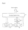
- Fig. 2 is a block diagram of a data output with decoding circuit using a capacitive input keyboard, to illustrate a typical application environment.
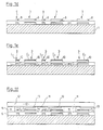
- FIG. 1 the partial figures of which correspond to different successive process stages, specifically for the case of a matrix arrangement of capacitors for a capacitive key arrangement, such as are used for input devices of data processing systems.
- the lower capacitor electrodes or coverings and associated connecting and supply lines are produced on a substrate or carrier plate 1, which can consist, for example, of hard paper or a polyester or polyimide film. In the exemplary embodiment shown, this takes place in a two-stage method illustrated by FIGS. 1 and 1 b.
- a substrate or carrier plate 1 which can consist, for example, of hard paper or a polyester or polyimide film.
- the carrier or substrate plate 1 is screen-printed with a metallizable paste 2 in accordance with a layout desired for the capacitor regions 3 and the conductor track regions 4.
- the metallizable paste 2 is then metallized in an electroless chemical bath, as indicated at 5 in FIG. 1.
- solderable metallizations for example made of copper or nickel, form the lower capacitor electrodes or coatings C1 in the capacitor regions 3, and the actual conductor paths L1 in the regions of the conductor tracks 4.
- An alternative way of producing the lower capacitor electrodes in the areas 3 and the conductor tracks in the areas 4 would be the use of a subtractive technique, in which the entire substrate is lined with metal, for example copper, by selective etching, for example using the light printing process in the desired manner Negative layout made photoresist etching masks, the capacitor electrodes C1 and the conductor tracks L1 would be produced.
- the dielectric layers for the capacitors are now produced according to FIG. 1c.
- the entire circuit is printed over the entire area with a screen-printable dielectric material.
- a screen-printable composition is used for this, which comprises a dispersion of dielectric particles such as ZnO, A1 2 0 3 , SrTi0 3 or BaTi0 3 in a curable polymer material, such as polyurethane resin or other resins, such as polyester, epoxy resin, melamine formaldehyde resin contains. 1, both the capacitor areas 3 and the conductor track areas 4 and also the spaces between them are printed over the entire area with the dielectric material.
- only the capacitor areas 3 can initially be selectively printed with the dielectric mass, while the conductor track surfaces and / or the spaces for level equalization and functional insulation are printed with other pastes, preferably with a lower dielectric constant, in order to reduce the capacitance of the conductor tracks as much as possible and to obtain the largest possible jump in capacitance when the capacitors are switched on or off as the desired switching criterion.
- the dispersion used according to the invention as a dielectric material on a polymer resin ba sis can be cured at relatively low temperatures in the range between about 150 and about 230 ° C, which is a significant advantage over the known cermet capacitors made with ceramic or glass frit pastes, for which baking temperatures of around 1,000 ° C are required, and in particular enables the use of the cheaper and less brittle-brittle substrate materials mentioned.
- the next step is the production of the second or upper capacitor electrodes, advantageously in connection with the production of a second conductor level as supply lines and connecting lines for these upper capacitor coatings.
- this takes place in a two-stage process according to FIGS. 1 and 1e.
- a second dielectric layer 8 is first prepared in accordance with the layout required for the capacitor regions 3 and conductor path regions 9 of an upper, second conductor level (which for the sake of simplicity are assumed in the exemplary embodiment shown to overlap with the conductor path regions 4 of the lower conductor level) the previously applied dielectric printing 6 (Fig. 1c) is screen printed.
- the dielectric layer 8 can be of the same or similar composition as the dielectric layer 6, with the difference, however, that it contains an activator based on palladium, as a result of which this second dielectric layer 8 can be metallized without current.
- a metallization activator or catalyst elemental palladium, for example in a content of 0.1%, can preferably be contained in the dielectric material 8, or else a palladium compound, such as PdC1 2 ; If such a Pd connection is used, however, after the baking of the layer, the connection would have to be converted into elementary Pd in a suitable manner, for example by treatment in a chemical bath, in order to ensure the desired activation of the second dielectric layer 8 for the subsequent electroless metallization.
- this second dielectric layer 8 can now be carried out in a subsequent method step according to FIG Pretreatment (with initial incorporation of elemental Pd as an activation catalyst) or after the aforementioned chemical reduction pretreatment (with initial use of a palladium compound as an activation component) can be metallized in an electroless plating bath, as indicated at 10 in Fig. 1e.
- Pretreatment with initial incorporation of elemental Pd as an activation catalyst
- chemical reduction pretreatment with initial use of a palladium compound as an activation component
- the second or upper capacitor electrodes or coatings C2 are formed in the capacitor regions 3 and the conductor paths L2 of the upper or second conductor level are formed in the conductor path regions 9.
- the capacitor electrodes C2 and upper conductor tracks L2 could finally also be produced in one step by printing with an electrically conductive screen printing paste, for example silver or nickel paste, instead of the two-stage method according to FIGS. 1d and 1e for the preferred electroless metallization.
- an electrically conductive screen printing paste for example silver or nickel paste
- the free spaces between the capacitor areas C2 and the conductor tracks L2 could, for example, be printed with the same or a similar screen printing paste of the same or different (smaller) dielectric constant, as a result of which a practically flat surface would be obtained, since the layer thickness of the metallizations 10 is of the order of less than 10 IJ .m lies.
- An insulating varnish could be applied over the entire surface (excluding the connection points) as the outer protective and passivation layer.
- the metal layers obtained in the preferred electroless metallization used to produce the capacitor electrodes and / or the conductor tracks are fully solderable and can be connected directly to chip components.
- the metal layers obtained by electroless metallization also have the advantage of particularly good adhesion due to the direct intimate contact with the dielectric layers that carry them.
- FIG. 1f forms a preferred area of application of the capacitor circuits according to the invention produced in pressure circuit technology.
- a larger number of capacitor areas 3 are provided, which are arranged in matrix form in accordance with a keypad customary for input keyboards.
- the spaces between the capacitor coverings C2 and the conductor tracks L2 of the upper level are not filled, and the respective connection leads L2 to the capacitor electrodes C2 are connected with them not directly connected.
- spacing elements 11 are introduced onto the lower, first dielectric layer 6 at suitable locations in spaces between the capacitor regions 3 and the conductor tracks L2 of the upper conductor level (but not between a respective capacitor coating C2 and its associated connecting line L2).
- This can preferably be a one-piece spacing film 11 with corresponding cutouts in the areas of the capacitors C2 and connecting lines L2 to be contacted.
- the spacer film 11 can be, for example, a polyethylene or polyester film.
- An outer film 12 covering the entire matrix arrangement is then placed over this spacer film 11 and supported by it, which has metallic bridging contacts 13, for example made of nickel, silver and, associated with the respective capacitor electrodes C2 and connecting lines L2 on the underside thereof in the areas corresponding to the recesses in the spacer film 11 preferably printed from gold.
- the contact film 12 can also consist of polyethylene or polyester, for particularly high-temperature applications also made of polyimide.
- the height (layer thickness) of the spacer film 11 is dimensioned such that the bridging contacts 13 are lifted from the capacitor electrodes C2 and the associated connecting lines L2 in the normal idle state.
- Fig. 2 illustrates a typical application environment of such a capacitive input keyboard, in the form of a block diagram of a data output with decoding circuit.
- the actual decoding circuit is designated by 14, 15 is a multiplexer circuit which is connected to the decoding circuit via a capacitive interface device 16.
- a capacitive keyboard matrix is indicated, which can be designed according to the embodiment of the invention described above.
- the data output is indicated, the data and effect flow between the different parts of the overall arrangement is indicated by the arrows.
Landscapes
- Engineering & Computer Science (AREA)
- Power Engineering (AREA)
- Microelectronics & Electronic Packaging (AREA)
- Manufacturing & Machinery (AREA)
- Parts Printed On Printed Circuit Boards (AREA)
- Fixed Capacitors And Capacitor Manufacturing Machines (AREA)
Claims (22)
Applications Claiming Priority (2)
| Application Number | Priority Date | Filing Date | Title |
|---|---|---|---|
| DE19813143995 DE3143995A1 (de) | 1981-11-05 | 1981-11-05 | Dickschichtkondensator in druckschaltungstechnik |
| DE3143995 | 1981-11-05 |
Publications (3)
| Publication Number | Publication Date |
|---|---|
| EP0078935A2 EP0078935A2 (fr) | 1983-05-18 |
| EP0078935A3 EP0078935A3 (en) | 1985-10-02 |
| EP0078935B1 true EP0078935B1 (fr) | 1989-01-11 |
Family
ID=6145715
Family Applications (1)
| Application Number | Title | Priority Date | Filing Date |
|---|---|---|---|
| EP82109533A Expired EP0078935B1 (fr) | 1981-11-05 | 1982-10-15 | Condensateur à film épais par la technique des circuits imprimés |
Country Status (4)
| Country | Link |
|---|---|
| US (1) | US4555745A (fr) |
| EP (1) | EP0078935B1 (fr) |
| JP (1) | JPS58180013A (fr) |
| DE (1) | DE3143995A1 (fr) |
Families Citing this family (25)
| Publication number | Priority date | Publication date | Assignee | Title |
|---|---|---|---|---|
| DE3143995A1 (de) * | 1981-11-05 | 1983-05-19 | Preh, Elektrofeinmechanische Werke, Jakob Preh, Nachf. Gmbh & Co, 8740 Bad Neustadt | Dickschichtkondensator in druckschaltungstechnik |
| EP0260665A3 (fr) * | 1986-09-18 | 1989-03-29 | Siemens Aktiengesellschaft | Procédé de fabrication d'un composant électrique construit sous forme de couche |
| BR8907268A (pt) * | 1988-12-24 | 1991-03-12 | Technology Aplications Company | Processo de efetuar uma conexao eletrica,placa de circuito impresso, processo de produzir uma almofada de contato,processo de produzir um capacitor,circuito impresso e processo de aplicar uma camada em um padrao desejado a um substrato |
| US5072378A (en) * | 1989-12-18 | 1991-12-10 | Storage Technology Corporation | Direct access storage device with independently stored parity |
| US5867363A (en) * | 1992-09-18 | 1999-02-02 | Pinnacle Research Institute, Inc. | Energy storage device |
| US5800857A (en) * | 1992-09-18 | 1998-09-01 | Pinnacle Research Institute, Inc. | Energy storage device and methods of manufacture |
| US5711988A (en) * | 1992-09-18 | 1998-01-27 | Pinnacle Research Institute, Inc. | Energy storage device and its methods of manufacture |
| US5464453A (en) * | 1992-09-18 | 1995-11-07 | Pinnacle Research Institute, Inc. | Method to fabricate a reliable electrical storage device and the device thereof |
| EP0662248A4 (fr) * | 1992-09-18 | 2000-10-25 | Pinnacle Research Inst Inc | Dispositif d'accumulation d'energie et son procede de fabrication |
| US5384685A (en) * | 1992-09-18 | 1995-01-24 | Pinnacle Research Institute, Inc. | Screen printing of microprotrusions for use as a space separator in an electrical storage device |
| US5821033A (en) * | 1992-09-18 | 1998-10-13 | Pinnacle Research Institute, Inc. | Photolithographic production of microprotrusions for use as a space separator in an electrical storage device |
| US5382928A (en) * | 1993-01-22 | 1995-01-17 | The Whitaker Corporation | RF filter having composite dielectric layer and method of manufacture |
| US5980977A (en) * | 1996-12-09 | 1999-11-09 | Pinnacle Research Institute, Inc. | Method of producing high surface area metal oxynitrides as substrates in electrical energy storage |
| US6935002B1 (en) * | 1997-10-13 | 2005-08-30 | Murata Manufacturing Co., Ltd. | Method of manufacturing a nonreciprocal circuit device |
| US6618238B2 (en) * | 1998-04-01 | 2003-09-09 | Polyclad Laminates, Inc. | Parallel plate buried capacitor |
| US6021050A (en) * | 1998-12-02 | 2000-02-01 | Bourns, Inc. | Printed circuit boards with integrated passive components and method for making same |
| DE19902769A1 (de) * | 1999-01-25 | 2000-07-27 | Philips Corp Intellectual Pty | Keramisches, passives Bauelement |
| DE19939483A1 (de) * | 1999-08-20 | 2001-03-08 | Philips Corp Intellectual Pty | Passives Bauelement mit Verbundwerkstoff |
| CN100380540C (zh) * | 2001-11-26 | 2008-04-09 | 希普利公司 | 介电结构 |
| US6661642B2 (en) * | 2001-11-26 | 2003-12-09 | Shipley Company, L.L.C. | Dielectric structure |
| US7056800B2 (en) * | 2003-12-15 | 2006-06-06 | Motorola, Inc. | Printed circuit embedded capacitors |
| KR100586963B1 (ko) * | 2004-05-04 | 2006-06-08 | 삼성전기주식회사 | 유전체 형성용 조성물, 이로 제조된 캐패시터층 및 이를포함하는 인쇄회로기판 |
| EP3091821A1 (fr) * | 2015-05-08 | 2016-11-09 | AT & S Austria Technologie & Systemtechnik Aktiengesellschaft | Carte de circuit imprimé |
| DE102015113694B4 (de) * | 2015-08-19 | 2021-09-09 | Preh Gmbh | Kapazitives Bedienelement mit verbesserter Störunanfälligkeit |
| KR102440363B1 (ko) * | 2017-08-11 | 2022-09-05 | 삼성전자주식회사 | 필름 프레임, 디스플레이 기판 제조 시스템 및 디스플레이 기판 제조 방법 |
Family Cites Families (22)
| Publication number | Priority date | Publication date | Assignee | Title |
|---|---|---|---|---|
| GB706067A (fr) * | 1900-01-01 | |||
| GB584672A (en) * | 1944-01-14 | 1947-01-21 | Erich Schaefer | Improvements in or relating to electrical condensers having plastic film dielectrics |
| FR1051606A (fr) * | 1951-02-07 | 1954-01-18 | Csf | Nouveau procédé de fabrication de matières isolantes à constante diélectrique élevée et leur application à la fabrication de condensateurs |
| US2934479A (en) * | 1957-01-22 | 1960-04-26 | Leon L Deer | Process for masking printed circuits before plating |
| US3310432A (en) * | 1963-07-11 | 1967-03-21 | Corning Glass Works | Method for applying electrical conductors on a smooth vitreous surface and article |
| US3481777A (en) * | 1967-02-17 | 1969-12-02 | Ibm | Electroless coating method for making printed circuits |
| US3660328A (en) * | 1970-07-27 | 1972-05-02 | Pfizer | Dielectric films |
| DE2132935C3 (de) * | 1971-07-02 | 1978-07-20 | Licentia Patent-Verwaltungs-Gmbh, 6000 Frankfurt | Elektrischer, im Siebdruckverfahren hergestellter Kondensator |
| JPS49105151A (fr) * | 1973-02-13 | 1974-10-04 | ||
| DE2434390A1 (de) * | 1973-07-17 | 1975-02-27 | Alphameric Holdings Ltd | Tastatur |
| DD114315A1 (fr) * | 1974-07-18 | 1975-07-20 | ||
| US3996502A (en) * | 1975-06-02 | 1976-12-07 | Zenith Radio Corporation | Thick film capacitors |
| JPS5810862B2 (ja) * | 1976-06-18 | 1983-02-28 | 株式会社東芝 | 厚膜集積回路装置 |
| US4090229A (en) * | 1976-09-30 | 1978-05-16 | Becton, Dickinson Electronics Company | Capacitive key for keyboard |
| US4182781A (en) * | 1977-09-21 | 1980-01-08 | Texas Instruments Incorporated | Low cost method for forming elevated metal bumps on integrated circuit bodies employing an aluminum/palladium metallization base for electroless plating |
| DE2841742A1 (de) * | 1978-09-26 | 1980-04-03 | Draloric Electronic | Kapazitives netzwerk |
| JPS55130127A (en) * | 1979-03-30 | 1980-10-08 | Matsushita Electric Ind Co Ltd | Printed capacitor and method of fabricating same |
| JPS6052567B2 (ja) * | 1979-10-29 | 1985-11-20 | 松下電器産業株式会社 | 厚膜コンデンサおよびその製造方法 |
| JPS56124223A (en) * | 1980-03-05 | 1981-09-29 | Tdk Electronics Co Ltd | Method of forming electrode for electronic part |
| JPS56130911A (en) * | 1980-03-17 | 1981-10-14 | Tdk Electronics Co Ltd | Method of forming electrode of electronic component |
| US4327126A (en) * | 1980-11-10 | 1982-04-27 | Ralph Ogden | Method of making printed circuit boards |
| DE3143995A1 (de) * | 1981-11-05 | 1983-05-19 | Preh, Elektrofeinmechanische Werke, Jakob Preh, Nachf. Gmbh & Co, 8740 Bad Neustadt | Dickschichtkondensator in druckschaltungstechnik |
-
1981
- 1981-11-05 DE DE19813143995 patent/DE3143995A1/de active Granted
-
1982
- 1982-09-28 US US06/425,519 patent/US4555745A/en not_active Expired - Fee Related
- 1982-10-15 EP EP82109533A patent/EP0078935B1/fr not_active Expired
- 1982-11-05 JP JP57193539A patent/JPS58180013A/ja active Pending
Also Published As
| Publication number | Publication date |
|---|---|
| DE3143995C2 (fr) | 1992-08-20 |
| EP0078935A3 (en) | 1985-10-02 |
| US4555745A (en) | 1985-11-26 |
| EP0078935A2 (fr) | 1983-05-18 |
| DE3143995A1 (de) | 1983-05-19 |
| JPS58180013A (ja) | 1983-10-21 |
Similar Documents
| Publication | Publication Date | Title |
|---|---|---|
| EP0078935B1 (fr) | Condensateur à film épais par la technique des circuits imprimés | |
| DE3738343C2 (fr) | ||
| DE3700910A1 (de) | Verfahren zum aufbau elektrischer schaltungen auf einer grundplatte | |
| DE1817434B2 (de) | Verfahren zur Herstellung einer elektrischen Leitungsanordnung | |
| DE112006000519B4 (de) | Integrierter Dünnschicht-Kondensator mit optimierter Temperaturkennlinie | |
| EP2170026B1 (fr) | Substrat en céramique et métal pour circuits ou modules électriques, procédé de fabrication d'un tel substrat ainsi que module doté d'un tel substrat | |
| DE2924292A1 (de) | Keramikkoerper mit einer metallisierten schicht | |
| DE3605160C2 (de) | Verfahren zur Herstellung einer keramischen Leiterplatte | |
| DE19542365A1 (de) | Verfahren zur Herstellung eines vielschichtigen keramischen Elektronikbauteils | |
| DE2251829A1 (de) | Verfahren zur herstellung metallisierter platten | |
| EP0073904B1 (fr) | Procédé pour la fabrication de circuits imprimés | |
| DE3022268A1 (de) | Traeger fuer ein netz zur verbindung von elektronischen bauelementen und verfahren zu seiner herstellung | |
| EP0071003B1 (fr) | Méthode pour la fabrication de circuits imprimés | |
| DE19521737C2 (de) | Verfahren zur Herstellung eines in einen gesinterten Körper integrierten Widerstands und Verfahren zur Herstellung einer Mehrschichtkeramik | |
| DE2146328A1 (de) | Leiterplatte | |
| DE102004047007B4 (de) | Verfahren für das Herstellen eines Keramiksubstrats für elektronische Dünnschicht-Bauelemente | |
| EP1445795B1 (fr) | Procédé de fabrication de supports de circuits électriques comportant des composants électroniques passifs intégrés | |
| DE2303158A1 (de) | Verfahren zur herstellung von anschlussplatten | |
| EP0278485B1 (fr) | Méthode de fabrication d'une plaquette utilisable pour la digitalisation | |
| AT402871B (de) | Verfahren zur herstellung einer trägerplatte für elektrische schaltungen | |
| DE2013291C3 (de) | Verfahren zur Herstellung einer gedruckten Schaltungsplatte | |
| EP0214573A2 (fr) | Procédé d'intégration de résistances dans des réseaux conducteurs déposés chimiquement | |
| DE1915756C3 (de) | Verfahren zur Herstellung dimensionsgenauer Dickfilmstrukturen auf Substraten | |
| DE1115834B (de) | Quetschtrimmerkondensator | |
| DE102007036046A1 (de) | Planares elektronisches Modul |
Legal Events
| Date | Code | Title | Description |
|---|---|---|---|
| PUAI | Public reference made under article 153(3) epc to a published international application that has entered the european phase |
Free format text: ORIGINAL CODE: 0009012 |
|
| AK | Designated contracting states |
Designated state(s): FR GB IT NL |
|
| PUAL | Search report despatched |
Free format text: ORIGINAL CODE: 0009013 |
|
| AK | Designated contracting states |
Designated state(s): FR GB IT NL |
|
| 17P | Request for examination filed |
Effective date: 19851023 |
|
| 17Q | First examination report despatched |
Effective date: 19870227 |
|
| GRAA | (expected) grant |
Free format text: ORIGINAL CODE: 0009210 |
|
| AK | Designated contracting states |
Kind code of ref document: B1 Designated state(s): FR GB IT NL |
|
| ET | Fr: translation filed | ||
| ITF | It: translation for a ep patent filed |
Owner name: DR. ING. A. RACHELI & C. |
|
| RAP2 | Party data changed (patent owner data changed or rights of a patent transferred) |
Owner name: PREH-WERKE GMBH & CO. KG |
|
| GBT | Gb: translation of ep patent filed (gb section 77(6)(a)/1977) | ||
| NLT2 | Nl: modifications (of names), taken from the european patent patent bulletin |
Owner name: PREH-WERKE GMBH & CO. KG TE BAD NEUSTADT, BONDSREP |
|
| NLT1 | Nl: modifications of names registered in virtue of documents presented to the patent office pursuant to art. 16 a, paragraph 1 |
Owner name: PREH-WERKE GMBH & CO. KG TE BAD NEUSTADT, BONDSREP |
|
| PLBE | No opposition filed within time limit |
Free format text: ORIGINAL CODE: 0009261 |
|
| STAA | Information on the status of an ep patent application or granted ep patent |
Free format text: STATUS: NO OPPOSITION FILED WITHIN TIME LIMIT |
|
| 26N | No opposition filed | ||
| PG25 | Lapsed in a contracting state [announced via postgrant information from national office to epo] |
Ref country code: NL Effective date: 19900501 |
|
| NLV4 | Nl: lapsed or anulled due to non-payment of the annual fee | ||
| PGFP | Annual fee paid to national office [announced via postgrant information from national office to epo] |
Ref country code: GB Payment date: 19900925 Year of fee payment: 9 |
|
| PGFP | Annual fee paid to national office [announced via postgrant information from national office to epo] |
Ref country code: FR Payment date: 19901009 Year of fee payment: 9 |
|
| ITTA | It: last paid annual fee | ||
| PG25 | Lapsed in a contracting state [announced via postgrant information from national office to epo] |
Ref country code: GB Effective date: 19911015 |
|
| GBPC | Gb: european patent ceased through non-payment of renewal fee | ||
| PG25 | Lapsed in a contracting state [announced via postgrant information from national office to epo] |
Ref country code: FR Effective date: 19920630 |
|
| REG | Reference to a national code |
Ref country code: FR Ref legal event code: ST |