EP0078084A2 - Montage avec élément de lissage commutable - Google Patents
Montage avec élément de lissage commutable Download PDFInfo
- Publication number
- EP0078084A2 EP0078084A2 EP82201320A EP82201320A EP0078084A2 EP 0078084 A2 EP0078084 A2 EP 0078084A2 EP 82201320 A EP82201320 A EP 82201320A EP 82201320 A EP82201320 A EP 82201320A EP 0078084 A2 EP0078084 A2 EP 0078084A2
- Authority
- EP
- European Patent Office
- Prior art keywords
- capacitor
- resistor
- output terminal
- amplifier
- voltage
- Prior art date
- Legal status (The legal status is an assumption and is not a legal conclusion. Google has not performed a legal analysis and makes no representation as to the accuracy of the status listed.)
- Granted
Links
Images
Classifications
-
- H—ELECTRICITY
- H03—ELECTRONIC CIRCUITRY
- H03L—AUTOMATIC CONTROL, STARTING, SYNCHRONISATION OR STABILISATION OF GENERATORS OF ELECTRONIC OSCILLATIONS OR PULSES
- H03L7/00—Automatic control of frequency or phase; Synchronisation
- H03L7/06—Automatic control of frequency or phase; Synchronisation using a reference signal applied to a frequency- or phase-locked loop
- H03L7/08—Details of the phase-locked loop
- H03L7/10—Details of the phase-locked loop for assuring initial synchronisation or for broadening the capture range
- H03L7/107—Details of the phase-locked loop for assuring initial synchronisation or for broadening the capture range using a variable transfer function for the loop, e.g. low pass filter having a variable bandwidth
-
- H—ELECTRICITY
- H03—ELECTRONIC CIRCUITRY
- H03F—AMPLIFIERS
- H03F1/00—Details of amplifiers with only discharge tubes, only semiconductor devices or only unspecified devices as amplifying elements
- H03F1/56—Modifications of input or output impedances, not otherwise provided for
-
- H—ELECTRICITY
- H03—ELECTRONIC CIRCUITRY
- H03F—AMPLIFIERS
- H03F3/00—Amplifiers with only discharge tubes or only semiconductor devices as amplifying elements
- H03F3/34—DC amplifiers in which all stages are DC-coupled
-
- H—ELECTRICITY
- H03—ELECTRONIC CIRCUITRY
- H03F—AMPLIFIERS
- H03F3/00—Amplifiers with only discharge tubes or only semiconductor devices as amplifying elements
- H03F3/50—Amplifiers in which input is applied to, or output is derived from, an impedance common to input and output circuits of the amplifying element, e.g. cathode follower
-
- H—ELECTRICITY
- H03—ELECTRONIC CIRCUITRY
- H03F—AMPLIFIERS
- H03F3/00—Amplifiers with only discharge tubes or only semiconductor devices as amplifying elements
- H03F3/72—Gated amplifiers, i.e. amplifiers which are rendered operative or inoperative by means of a control signal
-
- H—ELECTRICITY
- H03—ELECTRONIC CIRCUITRY
- H03F—AMPLIFIERS
- H03F2203/00—Indexing scheme relating to amplifiers with only discharge tubes or only semiconductor devices as amplifying elements covered by H03F3/00
- H03F2203/72—Indexing scheme relating to gated amplifiers, i.e. amplifiers which are rendered operative or inoperative by means of a control signal
- H03F2203/7221—Indexing scheme relating to gated amplifiers, i.e. amplifiers which are rendered operative or inoperative by means of a control signal the gated amplifier being switched on or off by a switch at the output of the amplifier
Definitions
- the invention relates to a circuit arrangement for transmitting a DC voltage with a switchable smoothing element located between an input terminal and an output terminal against a reference potential, which consists of at least one series resistor and behind it in the shunt arm a first capacitor, which may be in series with a first resistor, and a second capacitor, optionally connected in series with a second resistor, can be connected, which can be connected to the output terminal to increase the time constant.
- a changing voltage is normally transmitted to regulate a voltage controlled oscillator.
- the second capacitor is switched off, there is usually a different voltage on it than on the first capacitor.
- a charging or discharging current flows to it, and accordingly there is a surge which affects the transmitted voltage and which can have disadvantageous consequences.
- the oscillator can get out of the capture range, which causes a new switchover. The oscillator catches up again, etc. This takes a long time until the control loop has finally switched to the slow time constant.
- the invention has for its object to avoid this surge.
- This object is achieved according to the invention in that with the output terminal the input of an amplifier with a high input impedance and with an amplification factor of is connected at least approximately 1, the output of which is connected to the second capacitor.
- the output of the amplifier is connected to an output terminal of a switch, the switchable tongue of which is connected to the second capacitor, and the other output terminal of which is connected to the output terminal of the smoothing filter.
- the second capacitor is connected to the output terminal via the second resistor, the amplifier is connected in parallel with the second resistor, and the amplifier is switched between the gain factor zero and at least approximately 1.
- a changeover switch in the branch of the smoothing capacitor is not required; the switchover is effected by a control variable which switches the amplifier between the gain factor 1 and zero.
- the voltage of the second capacitor is also controlled with the voltage of the first capacitor, so that no current flows through the second resistor and the second resistor is ineffective for the smoothing filter.
- the second capacitor is connected to the smoothing filter via the resistor. This resistance need not be great, such that the second capacitor is connected practically directly to the output terminal.
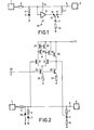
- a control voltage source 1 generates a DC voltage on the order of a few volts, e.g. 6 volts + 2 volts supplied. This is fed via a series resistor 2 to a shunt branch connected to ground, which contains the series connection of a first capacitor 3 and an associated series resistor 4. This branch may also contain other parallel branches with a similar structure or a parallel capacitor without a series resistor.
- the voltage occurring at the connection point of the resistors 2 and 4 is fed to the output terminal 5 and from there to a stage to be regulated, for example a voltage-dependent controlled oscillator 6.
- a resistor 7 is also connected to the terminal 5, which is connected to the one changeover contact 8 of a changeover switch 9, the tongue 10 of which is connected to ground via a second capacitor 11 of, for example, 4.7 / uF and possibly a resistor 12.
- the resistor 7 and possibly the resistor 12 is a second resistor in the circuit of the capacitor 11 when the latter is effective in the position of the tongue 10 of the switch 9 in the smoothing filter (not shown).
- the high-resistance input of an amplifier 13 is connected to the DC voltage line, to which the capacitor 3 is connected via the resistor 4, and is connected between a supply terminal + U of 12 volts and ground. Its low-resistance output is connected to the second terminal 14 of the switch 9. The same voltage occurs at this terminal 14 with low impedance, which is present at the series connection of capacitor 3 and resistor 4.
- the amplification factor of the amplifier 13 thus corresponds at least approximately to 1. This voltage is supplied to the capacitor 11 at every moment in the position of the tongue 10 of the switch 9 shown. If the switch 9 is then switched over, this voltage is transmitted from the capacitor 11 to the output terminal 5, it being evident that no disturbing voltage change can result.
- the changeover switch 9 can be saved and the capacitor 11 can remain permanently connected to the output of the amplifier 13 and also also to the resistor 7 if the amplifier 13 can be switched between the gain 1 and zero by means of a switching voltage supplied with a broken line terminal 15.
- the contacts 8 and 14 are then in permanent connection with the tongue 10. With the degree of amplification 1, the above-mentioned transmission of the voltage from the capacitor 3 to the capacitor 11 results. Then there is no voltage difference between the capacitor 11 and the output terminal 5, and accordingly overflows the resistor 7 no current: the capacitor 11 is therefore not effective in charging and discharging and smoothing the voltage at the output terminal 5.
- the amplifier 13 is switched to zero gain, its output becomes high-impedance, and the capacitor 11 is connected via the resistor 7 to the output terminal 5 and is effective in the smoothing filter.
- the resistor 7 can have a low value; because with effective amplifier 13 is due to him no voltage, so that it does not cause any stress in the circuit.
- FIG. 2 An embodiment of this circuit according to the invention, which operates without switching, is shown in FIG. 2, in which the same parts are again provided with the same reference numbers as in FIG. 1.
- a further capacitor 20 is connected in parallel with the series connection of the first capacitor 3 and the first resistor 4 to improve the smoothing properties.
- the voltage occurring at the output of the resistor 2 and at the terminal 5 is fed to the base of a first npn transistor 21, the emitter of which is connected to the emitter of a second npn transistor 22 and to the collector of a third npn transistor 23.
- the base of transistor 23 is connected to a terminal 24, to which a switching voltage V is supplied; the emitter of transistor 23 is connected to ground via a resistor 25.
- the collectors of the transistors 21 and 22 are connected via the collector-emitter paths of two pnp transistors 27 and 28 to the 12 V supply source + U.
- the collector of transistor 27 is also at the base of a pnp transistor 29, the emitter of which is connected to the connected bases of transistors 27 and 28 and the collector of which is connected to ground.
- the transistors 27, 28 and 29 form a current mirror circuit by means of which the collector currents of the transistors 21 and 22 are kept the same.
- the collector of transistor 22 is further connected to the base of an npn transistor 30, the emitter of which controls the base of an npn transistor 31, the emitter of which is connected to the base of transistor 22.
- the collectors of transistors 30 and 31 are connected to + U.
- the collector-emitter path of an npn transistor 32 also lies between the base of transistor 22 and ground Emitter resistor 33.
- the base of transistor 32 is connected to terminal 24.
- the connection point of the emitter of transistor 31 to the collector of transistor 32 and the base of transistor 22 is further connected to the connection point of capacitor 11 and resistor 7.
- the transistors 23 and 32 act as current sources on the one hand for the differential amplifier 21, 22 and on the other hand for the emitter current branch of the double emitter follower 30, 31.
- This circuit ensures that the voltages at the bases of the transistors 21 and 22 are always exactly the same, the input of transistor 21 being very high-resistance and the base connection of transistor 22 being very low-resistance due to the action of emitter followers 30, 31.
- the voltage occurring at the output terminal 5 is therefore always transferred to the capacitor 11; there is no voltage difference across resistor 7. If necessary, the capacitor 11 is recharged by the transistors 30, 31, 32, the maximum discharge current being determined by the current source 32, 33.
- the amplifier with the transistors 21 to 32 is currentless and ineffective. Then the capacitor 11 is connected with a series resistor 12 via the resistor 7 at the output terminal 5 and thus causes an increase in the time constant of the smoothing element.
Landscapes
- Engineering & Computer Science (AREA)
- Power Engineering (AREA)
- Networks Using Active Elements (AREA)
- Amplifiers (AREA)
- Direct Current Feeding And Distribution (AREA)
- Control Of Electrical Variables (AREA)
- Filters And Equalizers (AREA)
Applications Claiming Priority (2)
| Application Number | Priority Date | Filing Date | Title |
|---|---|---|---|
| DE19813142612 DE3142612A1 (de) | 1981-10-28 | 1981-10-28 | Schaltungsanordnung mit einem umschaltbaren glaettungsglied |
| DE3142612 | 1981-10-28 |
Publications (3)
| Publication Number | Publication Date |
|---|---|
| EP0078084A2 true EP0078084A2 (fr) | 1983-05-04 |
| EP0078084A3 EP0078084A3 (en) | 1984-10-10 |
| EP0078084B1 EP0078084B1 (fr) | 1988-09-21 |
Family
ID=6144946
Family Applications (1)
| Application Number | Title | Priority Date | Filing Date |
|---|---|---|---|
| EP82201320A Expired EP0078084B1 (fr) | 1981-10-28 | 1982-10-22 | Montage avec élément de lissage commutable |
Country Status (4)
| Country | Link |
|---|---|
| US (1) | US4849663A (fr) |
| EP (1) | EP0078084B1 (fr) |
| JP (1) | JPS5882320A (fr) |
| DE (2) | DE3142612A1 (fr) |
Cited By (1)
| Publication number | Priority date | Publication date | Assignee | Title |
|---|---|---|---|---|
| AT513104B1 (de) * | 2012-07-10 | 2015-11-15 | Felix Dipl Ing Dr Himmelstoss | Vorrichtung zur Konstanthaltung der Frequenz eines spannungsgesteuerten Oszillators |
Families Citing this family (7)
| Publication number | Priority date | Publication date | Assignee | Title |
|---|---|---|---|---|
| JPH02174414A (ja) * | 1988-12-27 | 1990-07-05 | Hitachi Ltd | 半導体集積回路装置 |
| JP2748676B2 (ja) * | 1990-09-19 | 1998-05-13 | 日本電気株式会社 | Pll回路 |
| US5444312A (en) * | 1992-05-04 | 1995-08-22 | Compaq Computer Corp. | Soft switching circuit for audio muting or filter activation |
| US5394028A (en) * | 1992-06-26 | 1995-02-28 | Motorola, Inc. | Apparatus for transitioning between power supply levels |
| US5794130A (en) * | 1994-04-26 | 1998-08-11 | Funai Electric Engineering Company Limited | Wireless communication system having improved PLL circuits |
| DE19611219A1 (de) * | 1996-03-21 | 1997-09-25 | Fraunhofer Ges Forschung | Phasenregelschleife mit umschaltbarer Schleifenbandbreite |
| US5841324A (en) * | 1996-06-20 | 1998-11-24 | Harris Corporation | Charge-based frequency locked loop and method |
Family Cites Families (14)
| Publication number | Priority date | Publication date | Assignee | Title |
|---|---|---|---|---|
| US2828419A (en) * | 1954-10-11 | 1958-03-25 | Gen Electric | Automatic frequency control system |
| US3893034A (en) * | 1958-11-04 | 1975-07-01 | Bell Telephone Labor Inc | Smoothing circuits |
| US3287657A (en) * | 1963-04-09 | 1966-11-22 | Ericsson Telefon Ab L M | Phase controlled oscillator with a variable synchronizing range |
| US3408590A (en) * | 1966-10-31 | 1968-10-29 | Bell Telephone Labor Inc | Active hybrid filter using frequency emphasizing and attenuating networks |
| DE2159223A1 (de) * | 1971-11-30 | 1973-06-14 | Licentia Gmbh | Zeilensynchronisierschaltung mit umschaltbarer zeitkonstante fuer einen fernsehempfaenger |
| US3909735A (en) * | 1974-04-04 | 1975-09-30 | Ncr Co | Slow switch for bandwidth change in phase-locked loop |
| US4007429A (en) * | 1976-01-19 | 1977-02-08 | Gte International Incorporated | Phase-locked loop having a switched lowpass filter |
| JPS5923126B2 (ja) * | 1976-09-09 | 1984-05-31 | 日本電気株式会社 | しや断周波数可変濾波器 |
| US4142110A (en) * | 1977-04-07 | 1979-02-27 | Fa. Weber Lichtsteuergerate Kg. | Circuit to eliminate DC bias |
| US4156855A (en) * | 1978-01-26 | 1979-05-29 | Rca Corporation | Phase-locked loop with variable gain and bandwidth |
| GB2017444B (en) * | 1978-03-14 | 1982-05-26 | Secr Defence | Active filter network |
| US4540946A (en) * | 1980-06-06 | 1985-09-10 | National Research Development Corp. | Variable characteristic filters |
| JPS5843031U (ja) * | 1981-09-17 | 1983-03-23 | パイオニア株式会社 | 低域通過型フイルタ |
| US4482869A (en) * | 1982-04-13 | 1984-11-13 | Pioneer Electronic Corporation | PLL Detection circuit having dual bandwidth loop filter |
-
1981
- 1981-10-28 DE DE19813142612 patent/DE3142612A1/de not_active Withdrawn
-
1982
- 1982-10-22 EP EP82201320A patent/EP0078084B1/fr not_active Expired
- 1982-10-22 DE DE8282201320T patent/DE3279067D1/de not_active Expired
- 1982-10-25 JP JP57186220A patent/JPS5882320A/ja active Granted
-
1989
- 1989-01-06 US US07/294,964 patent/US4849663A/en not_active Expired - Fee Related
Cited By (1)
| Publication number | Priority date | Publication date | Assignee | Title |
|---|---|---|---|---|
| AT513104B1 (de) * | 2012-07-10 | 2015-11-15 | Felix Dipl Ing Dr Himmelstoss | Vorrichtung zur Konstanthaltung der Frequenz eines spannungsgesteuerten Oszillators |
Also Published As
| Publication number | Publication date |
|---|---|
| DE3279067D1 (en) | 1988-10-27 |
| EP0078084A3 (en) | 1984-10-10 |
| EP0078084B1 (fr) | 1988-09-21 |
| JPH0468810B2 (fr) | 1992-11-04 |
| US4849663A (en) | 1989-07-18 |
| JPS5882320A (ja) | 1983-05-17 |
| DE3142612A1 (de) | 1983-05-11 |
Similar Documents
| Publication | Publication Date | Title |
|---|---|---|
| DE3713376A1 (de) | Komparator mit erweitertem eingangsgleichtaktspannungsbereich | |
| EP0087175A1 (fr) | Circuit pour commander électroniquement le gain | |
| DE1812292C3 (de) | Schaltungsanordnung zur Verstärkungsregelung | |
| WO1997033365A1 (fr) | Amplificateur operationnel | |
| EP0078084B1 (fr) | Montage avec élément de lissage commutable | |
| EP0809350A1 (fr) | Oscillateur à quartz commandé numériquement et circuit oscillateur intégré monolithique | |
| DE2931922C2 (de) | "Schaltungsanordnung zum Speisen einer eine konstante Betriebsspannung liefernden Stromversorgungseinrichtung" | |
| DE3901983A1 (de) | Stifttreiberschaltung | |
| DE2946952C2 (fr) | ||
| DE3539379C2 (de) | Monolithisch integrierte Steuerschaltung für die Umschaltung von Transistoren | |
| EP0106408B1 (fr) | Montage de circuit pour la commande du volume sonore | |
| DE3029895C2 (de) | Schaltungsanordnung zum Speisen einer eine konstante Betriebsspannung liefernden Stromversorgungseinrichtung | |
| DE2813856A1 (de) | Einstellbarer transistor-verstaerker | |
| DE2107714C3 (de) | Schaltung zum Umschalten der Resonanzfrequenzen elektrischer Schwingkreise | |
| DE3816140A1 (de) | Videosignalumschalter | |
| DE2006757C3 (de) | Elektrische Schaltungsanordnung zur stufenlosen Veränderung der Nachstellzeitkonstanten eines Reglers mit nachgebender Rückführung | |
| DE1537606C (de) | Gleichstromverstärker mit Schaltung zur Driftkompensation | |
| DE3418191C2 (fr) | ||
| DE1537606A1 (de) | Gleichstromverstaerker mit Schaltung zur Driftkompensation | |
| DE2711520B2 (de) | Belastungsschaltung für eine Signalquelle | |
| DE3043768C2 (de) | Spannungsfolger-Verstärker für eine kapazitive Last | |
| DE2931901C2 (de) | Monolithisch integrierter Schwellwertschalter | |
| DE3715731C2 (fr) | ||
| DE2246607A1 (de) | Schaltungsanordnung zur vergroesserung der wirksamen kapazitaet eines kondensators | |
| DE1814887B2 (de) | Transistorverstaerker |
Legal Events
| Date | Code | Title | Description |
|---|---|---|---|
| PUAI | Public reference made under article 153(3) epc to a published international application that has entered the european phase |
Free format text: ORIGINAL CODE: 0009012 |
|
| 17P | Request for examination filed |
Effective date: 19821022 |
|
| AK | Designated contracting states |
Designated state(s): DE FR GB IT |
|
| PUAL | Search report despatched |
Free format text: ORIGINAL CODE: 0009013 |
|
| AK | Designated contracting states |
Designated state(s): DE FR GB IT |
|
| 17Q | First examination report despatched |
Effective date: 19861107 |
|
| R17C | First examination report despatched (corrected) |
Effective date: 19870424 |
|
| RAP1 | Party data changed (applicant data changed or rights of an application transferred) |
Owner name: N.V. PHILIPS' GLOEILAMPENFABRIEKEN Owner name: PHILIPS PATENTVERWALTUNG GMBH |
|
| GRAA | (expected) grant |
Free format text: ORIGINAL CODE: 0009210 |
|
| AK | Designated contracting states |
Kind code of ref document: B1 Designated state(s): DE FR GB IT |
|
| REF | Corresponds to: |
Ref document number: 3279067 Country of ref document: DE Date of ref document: 19881027 |
|
| ITF | It: translation for a ep patent filed | ||
| ET | Fr: translation filed | ||
| GBT | Gb: translation of ep patent filed (gb section 77(6)(a)/1977) | ||
| PLBE | No opposition filed within time limit |
Free format text: ORIGINAL CODE: 0009261 |
|
| STAA | Information on the status of an ep patent application or granted ep patent |
Free format text: STATUS: NO OPPOSITION FILED WITHIN TIME LIMIT |
|
| 26N | No opposition filed | ||
| PGFP | Annual fee paid to national office [announced via postgrant information from national office to epo] |
Ref country code: GB Payment date: 19910809 Year of fee payment: 10 |
|
| PGFP | Annual fee paid to national office [announced via postgrant information from national office to epo] |
Ref country code: FR Payment date: 19911023 Year of fee payment: 10 |
|
| ITTA | It: last paid annual fee | ||
| PG25 | Lapsed in a contracting state [announced via postgrant information from national office to epo] |
Ref country code: GB Effective date: 19921022 |
|
| GBPC | Gb: european patent ceased through non-payment of renewal fee |
Effective date: 19921022 |
|
| PG25 | Lapsed in a contracting state [announced via postgrant information from national office to epo] |
Ref country code: FR Effective date: 19930630 |
|
| REG | Reference to a national code |
Ref country code: FR Ref legal event code: ST |
|
| PGFP | Annual fee paid to national office [announced via postgrant information from national office to epo] |
Ref country code: DE Payment date: 19951219 Year of fee payment: 14 |
|
| PG25 | Lapsed in a contracting state [announced via postgrant information from national office to epo] |
Ref country code: DE Effective date: 19970701 |