EP0077902A2 - Logique à transistors inverses bipolaires intégrée - Google Patents
Logique à transistors inverses bipolaires intégrée Download PDFInfo
- Publication number
- EP0077902A2 EP0077902A2 EP82108134A EP82108134A EP0077902A2 EP 0077902 A2 EP0077902 A2 EP 0077902A2 EP 82108134 A EP82108134 A EP 82108134A EP 82108134 A EP82108134 A EP 82108134A EP 0077902 A2 EP0077902 A2 EP 0077902A2
- Authority
- EP
- European Patent Office
- Prior art keywords
- transistor
- gate
- collector
- current source
- transistors
- Prior art date
- Legal status (The legal status is an assumption and is not a legal conclusion. Google has not performed a legal analysis and makes no representation as to the accuracy of the status listed.)
- Granted
Links
- 239000004065 semiconductor Substances 0.000 claims abstract description 19
- 239000013078 crystal Substances 0.000 claims abstract description 7
- 239000000463 material Substances 0.000 claims description 15
- 239000004020 conductor Substances 0.000 claims description 10
- 239000002184 metal Substances 0.000 claims description 4
- 230000003321 amplification Effects 0.000 claims description 3
- 238000003199 nucleic acid amplification method Methods 0.000 claims description 3
- 238000009792 diffusion process Methods 0.000 description 22
- 238000005516 engineering process Methods 0.000 description 16
- 238000002347 injection Methods 0.000 description 13
- 239000007924 injection Substances 0.000 description 13
- 230000000903 blocking effect Effects 0.000 description 8
- 239000010410 layer Substances 0.000 description 8
- 239000000243 solution Substances 0.000 description 7
- 238000000034 method Methods 0.000 description 5
- 238000004519 manufacturing process Methods 0.000 description 3
- 229920006395 saturated elastomer Polymers 0.000 description 3
- 230000005540 biological transmission Effects 0.000 description 2
- 238000013461 design Methods 0.000 description 2
- 230000002349 favourable effect Effects 0.000 description 2
- 238000012856 packing Methods 0.000 description 2
- 238000000926 separation method Methods 0.000 description 2
- 239000002356 single layer Substances 0.000 description 2
- 239000000758 substrate Substances 0.000 description 2
- 230000002411 adverse Effects 0.000 description 1
- 238000013475 authorization Methods 0.000 description 1
- 230000004888 barrier function Effects 0.000 description 1
- 230000015572 biosynthetic process Effects 0.000 description 1
- 238000010276 construction Methods 0.000 description 1
- 230000003247 decreasing effect Effects 0.000 description 1
- 230000001934 delay Effects 0.000 description 1
- 230000001419 dependent effect Effects 0.000 description 1
- 230000005611 electricity Effects 0.000 description 1
- 230000007613 environmental effect Effects 0.000 description 1
- 238000009472 formulation Methods 0.000 description 1
- 230000036039 immunity Effects 0.000 description 1
- 238000009413 insulation Methods 0.000 description 1
- 239000000203 mixture Substances 0.000 description 1
- 238000009738 saturating Methods 0.000 description 1
- 238000013519 translation Methods 0.000 description 1
Images

Classifications
-
- H—ELECTRICITY
- H10—SEMICONDUCTOR DEVICES; ELECTRIC SOLID-STATE DEVICES NOT OTHERWISE PROVIDED FOR
- H10D—INORGANIC ELECTRIC SEMICONDUCTOR DEVICES
- H10D84/00—Integrated devices formed in or on semiconductor substrates that comprise only semiconducting layers, e.g. on Si wafers or on GaAs-on-Si wafers
- H10D84/60—Integrated devices formed in or on semiconductor substrates that comprise only semiconducting layers, e.g. on Si wafers or on GaAs-on-Si wafers characterised by the integration of at least one component covered by groups H10D10/00 or H10D18/00, e.g. integration of BJTs
- H10D84/65—Integrated injection logic
-
- H—ELECTRICITY
- H03—ELECTRONIC CIRCUITRY
- H03K—PULSE TECHNIQUE
- H03K19/00—Logic circuits, i.e. having at least two inputs acting on one output; Inverting circuits
- H03K19/02—Logic circuits, i.e. having at least two inputs acting on one output; Inverting circuits using specified components
- H03K19/08—Logic circuits, i.e. having at least two inputs acting on one output; Inverting circuits using specified components using semiconductor devices
- H03K19/082—Logic circuits, i.e. having at least two inputs acting on one output; Inverting circuits using specified components using semiconductor devices using bipolar transistors
- H03K19/091—Integrated injection logic or merged transistor logic
Definitions
- the invention is based on a bipolar integrated transistor transistor logic according to the type of the main claim.
- ITL - inverter transistor logic - hereinafter briefly referred to as ITL - of this type, in which the base of the lateral current source transistor and the emitter of the gate transistor are connected to the same potential (ground potential), which means that the saturation state of the injector part (here a separate lateral transistor) which occurs during operation of the gate remains inevitable in I 2 L customary fashion and has all the disadvantages of the gate behavior.
- the local separation of the injector part and amplifier transistor has been completed, which in the sense of merged transistor logic has always been understood as a disadvantage in terms of space requirements.
- the bipolar integrated inverter transistor logic according to the invention with the characterizing features of the main claim has the advantage that the base potential of the lateral current source transistor is freely selectable. According to claim 2, the base potential of the lateral current source transistor can be set so that this transistor no longer operates in saturation mode even when the gate is conductive, so that the full current gain of the vertically upwardly amplifying gate transistor is available as gate current gain. If the lateral current source transistor is of the pnp type and the gate transistor of the npn type, the base potential of the current source transistor must be raised above the emitter potential of the gate transistor.
- the lateral current source transistor is of the NPN type and the gate transistor is of the PNP type, then the base potential of the current source transistor must be lowered below the emitter potential of the gate transistor. are If there are several gate transistors, they can be supplied with working currents from a single current source transistor which is provided with several collectors. The current source transistor then supplies approximately the same working currents for all gate transistors under all practical operating conditions. The saturation potentials at the collectors of these current source transistors are then so high compared to the gate reference potential that the opening voltages for the gate transistors are always reached. Further advantages result from the further subclaims 3 to 31 and from the description.
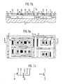
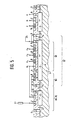
- FIGS. 1a and 1b schematically show a gripped section of a structure in conventional "mixing technology" without claiming to scale accuracy.
- FIG. 1a is the top view
- FIG. 1b is the sectional view identified in FIG. 1a
- FIG. 1c shows the electrical equivalent images of the structures shown in FIGS. 1a and 1b - on the left an I 2 L gate, on the right a bipolar vertical transistor (here of the npn type ).
- mixed media means that both the bipolar components (here vertical npn transistor), which are primarily suitable for analog circuits, and the I 2 L or I 3 L gates, which are suitable for digital circuits, are monolithically integrated on the same chip.
- bipolar components here vertical npn transistor
- I 2 L or I 3 L gates which are suitable for digital circuits
- mixed technology one usually starts from a manufacturing process that satisfies the more extensive and technically more difficult requirements for the properties of the analog components, and tries to meet the requirements with minimal process variants that do not adversely affect the properties of the analog components Properties of the digital gates. Numerous proposals for such process variants have become known in the literature, but only a few of them are currently on the way to technical and economic importance.
- I 2 L technology is also becoming increasingly important in the LSI area because the manufacturing processes are no longer subject to the extremely restrictive requirements for the analog elements and the process results can thus be optimized solely for the I 2 L properties .
- the invention brings a significant improvement in the effective gate current gain.
- the other advantages according to the invention are: improved gate speed and a largely prepared wiring system, the general disadvantages in this regard overcoming I 2 L and I 3 L circuits and preparing the wiring for the use of automatic design systems.
- FIG. 1b The sectional view of a typical mixed technology structure is shown schematically in FIG. 1b.
- a weakly n-doped layer 4 is applied epitaxially to a p-substrate 1 after pre-loading and prediffusion of later "buried" n + regions 2, 3.
- the active chip area is divided into epitaxial "wells" in such a way that the analog components - on the right in FIG. 1a and FIG. 1b - in essentially each individually and the I 2 L or I 3 L gates - on the left in FIG. 1a and FIG. 1b - come to lie in a tub as a whole.
- the n + diffusions 6 establish the electrical connection of the buried layers 2 and 3 to the semiconductor surface and provide in the I 2 L or .
- I 3 L part additionally for electrical shielding of the gates against each other.
- the n + flat diffusion 9 is sometimes used for shielding the gates from one another instead of the n deep diffusion 6 for reasons of space.
- the p-diffusions 7 form, among other things, the base zones for the current-amplifying transistors both in the analog part and in the I 2 L or I 3 L part.
- the injector zones 8 of the digital part also arise in the same diffusion step.
- the flat n + zones 9 are created, the emitter zones in the analog part the vertically downward working npn transistors and in the digital part the collector zones of the vertically upward working npn transistors (several collectors per transistor).
- the contact windows for electrical contacting of the individual zones are shown dark in the plan view according to FIG. 1a. Conductor paths have been omitted for reasons of clarity.
- npn transistor emitter - 7: base - 4, 3, 6: collector
- the vertically upwards working npn -Transistor (6, 2, 4: emitter - 7: base - 9: collector) in the digital part only moderate current amplifications (typically 3 to 10 per collector) - to be understood with cheap collector currents, which are different for the two transistors.
- the switching delay time is approximately constant, because here the approximately current-proportional diffusion capacity controls the switching behavior.
- this diffusion capacity is larger because of the minority storage in the high-resistance emitter region 4 than in the gates of the purely digital I 2 L technology built on a low-resistance epitaxial region, so that the. Mixing technology gates are much slower.
- saturation of the injector structure Miniorticianslic be in epitaxial region 4 additionally stored that need to be addressed in the depletion phase partially, which increases the operating time of the 'gate.
- the removal of the part of the diffusion capacity near the injector is hampered by the fact that the injector continuously supplies (increasing amount of) the current.
- the injector structure can no longer be regarded as a current source.
- Their low source voltage (diode forward voltage minus residual voltage) and the base rail resistances provide for an additional resistance-limited charging of the diffusion capacitance, so that the minimum switch-on delay possible with current source operation is not achieved, and finally in the conventional I 2 L or I 3 L structure due to the successive decrease in the injector current in the direction away from the injector, the last collector always switched on last.
- the additional delays from this are sometimes considerable and determine the maximum permissible clock frequency with clocked logic.
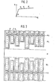
- the metallic injector lines IL 1 , IL 2 are difficult to cross due to electrical reasons of signal lines.
- the injectors are arranged in a row as shown, and gate fields are located on both sides of the injector lines, of which the gate fields GF and GF 2 are particularly marked in FIG. Depending on the need, there is a more or less wide wiring field VF between the gate fields.
- the conditions in the GF 2 gate field are shown as they typically occur:
- the gates are often longer than they should be for electrical and functional reasons, because not all available contact locations can be used to make wiring within the gate field easier . This is primarily a result of the gate position flush with the injector line.
- the space not used due to different gate lengths in the gate field cannot be used for other purposes (e.g. wiring tasks of the wiring field VF).
- the gate field GF 2 is shown again in the gate field GF, with only the electrically necessary gate lengths in the gate field GF to be used. An overall not optimal packing density of the gates becomes clear, which is usually due to the comparatively more difficult wiring of the I 2 L or.
- the solution according to the invention is mainly characterized by an electrical feature and by a geometric feature that describes the arrangement of the elements in the lay-out. In their overall sequence, further advantageous electrical and geometric designs are then possible.
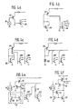
- the task of the lateral injection transistors (8: emitter - 4: base - 7: collector) of the conventional I 2 L or I 3 L structures according to FIG. 1 is to ensure that the working currents for the upward-amplifying gate transistors are as uniform as possible in the entire gate field To provide gates. So it is essentially the property of a constant current source, which in the form of the injector arrangement in is integrated into the gate in an apparently space-saving manner. The significant electrical shortcomings of this power source have been described. A current source that is far more electrically suitable for this task is obtained if, instead of the lateral injection transistor incorporated into the gate according to FIG. 1, a lateral transistor 40 that is electrically insulated from the vertically amplifying gate transistor is used as the current source (FIG. 5).
- FIGS. 4 and 2 The electrical advantages of the freely available base potential at the lateral current source transistor 40 can be seen from FIGS. 4 and 2.
- the base potential of this transistor 40 is initially set only sufficiently far above the reference potential by a voltage source 10, so that the mode of operation of the power supply for an overall circuit designed in this way does not differ from that Operating mode of the power supply of conventional I 2 L or I 3 L circuits would differentiate.
- the electrical sequence can be seen on the basis of the output characteristic of the lateral current source transistor in FIG. 2.
- the operating points for blocked or conductive gates have been set to points A 'and B' (compared to A and B in conventional technology).
- the current difference between the gate switching states has become negligibly small because the current source transistor 40 no longer has to operate in saturation mode even when the gate is conductive.
- the full current gain of the vertical step-up transistor 80 is thus available as a gate current gain. In conventional technology, the gate current gain would be reduced by approximately the quotient from current at operating point A to current at operating point A.
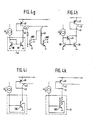
- the voltage source 10 in FIG. 4a can then be, for example, a diode 103 (FIG. 4d) through which the total base current of the lateral transistor and optionally one or more currents flow from partial collectors.
- the diode can in the simplest way consist of an inverter stage 101 of the gate field with a short circuit between the base and the collector (FIG. 5) or with a short circuit between the base and the collectors (see also FIGS. 4b and 4c or in a simplified representation in FIG. 4d).
- a reference current I o is compared either directly or, as in FIG. 4e, via a current mirror 41 with the current of a partial collector 42 of the lateral current source transistor 40.
- the potential of the node 43 is then set such that the base current amplifier (transistor 44) supplies the lateral current source transistor 40 with just as much base current that the current from the sub-collector 42 and thus also the currents from all other similar sub-collectors are just equal to the reference current I o is.
- the current ratio 41 is given a transmission ratio that deviates from 1: 1, then a current translation can also be generated between the reference current I 0 and the current from the partial collector 42.
- the current mirror 41 can again consist of inverter stages of the gate field, it also being possible to make the transmission ratio of the current mirror dependent on the current gain of the gate transistors by means of a base current amplifier 45 according to FIG. 4f.
- the exemplary embodiments according to FIGS. 4g and 4h differ from those according to FIGS. 4e and 4f in that the transistors 44 acting as base current amplifiers are omitted and in each case replaced by a short-circuit line which forms the base of the lateral current source transistor 40 with its sub-collector 42 at the node 43 connects.
- a single, vertically upward-amplifying transistor 900 with at least two collectors is used as the current mirror instead of the current mirror circuits comprising two or three transistors contained in FIGS. 4e and 4f, one (FIG. 4i) or a first interconnected group (FIG.
- the vertically upward amplifying transistor 900 can consist of a gate transistor of a gate array GF.
- Logic circuits according to the invention are largely insensitive to such voltage drops.
- the construction of the power sources provides for all gates approximately the same work flows under all practical operating conditions.
- the current sources are so high from the outset that the opening voltages for the gate transistors (vertical step-up transistors) are always reached. Additional voltage drops between the current source (partial collector) and the base of the gate transistor - for example caused by connecting n-bridges (46 in FIG. 4e) or the base path resistance of the gate transistor itself - can be permitted because there is sufficient voltage space available from the collector of the current source transistor 40 ( not so with a conventional injector). If, on the other hand, one assumes for the blocking case that the reference potential of a gate to be blocked is approximately 200 mV lower than the reference potential of the blocking gate located far away due to voltage drops on the buried layer 2 (FIG.
- the operating current is always fed to the gate via its base contact and is always intercepted at the base contact by a blocking gate, so that the locked gate is completely de-energized.
- the constant current supplying injector of conventional type is removed from the gate so that the barrier obstruction of the gate collectors close to the injector is eliminated.
- the minority-saturated injector volume of the gate is no longer available, so that the blocking delay caused thereby is eliminated.
- the resistance-limited (base rail resistance) charge of the diffusion capacities is eliminated because there is sufficient forward voltage available from the current source.
- the supply of the working current takes place conventionally from the electrically least favorable position on the narrow side of the elongated gate strip (FIG. 3). According to the invention, there is always a more favorable position for the supply via the base contact B i (FIG. 5).
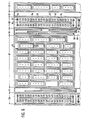
- FIG. 6 shows a simplified lay-out of a four-stage asynchronous frequency divider.
- the contact windows are marked with dots.
- the boundary lines of the gate collectors (emitter diffusion) in the gate strip and the conductor tracks have not been drawn in for the sake of clarity.
- Figure 7 shows the formal lay-out of the frequency divider stage. It shows the gate strips with their collector connections (x) and their base connections (o) as well as the conductive connections made of metal or polycrystalline semiconductor material (solid lines) and the bridges made of low-resistance, diffused semiconductor material (dashed lines).
- the one from the Gate fields at the top and bottom of the conductor tracks each lead to a partial collector of the lateral current source transistors 40.
- the current source transistors are electrically isolated lateral transistors and are therefore always completely enclosed by areas of insulation diffusion 51.
- the elongated emitter 52 of the transistor consisting of base diffusion material, is generally in the center line of the transistor.
- collectors 53 On both sides of the emitter 52 there is a large number of collectors 53, likewise made of material of the basic diffusion, to which the individual working currents for the gate field GF, driver stages and reference circuits are removed.
- At least one base connection 55 must be available for each current source transistor SQ.
- the electrical transistor base 54 is formed by the epitaxial material between the emitter 52 and the individual collectors 53. Their consistently good electrical contact to the base connection 55 determines the achievable uniformity of all collector currents.
- the gate field GF is therefore expediently constructed in a first rough structure from columns perpendicular to the longitudinal direction of the current source transistors SQ, the width of which is alternately dimensioned for three and four contact locations, the location for the (shielding) deep collector diffusion 58 (zone 6 in the 1 L part of FIGS. 1a and 1b). Circuitry and lay-out requirements then force one to break this rigid scheme: gates with different numbers of collector positions have to be inserted, and the rigid column formation almost never fits into the considerations of a sensible lay-out.
- Wiring in the gate field is only possible via a contact location of the gate for gate-crossing interconnects (conventionally the same way); the gap between the gates is available for gate-passing interconnects.
- two conductor tracks can be routed in parallel, both vertically and horizontally. In principle, this is also possible in a conventional manner, but because of the different type of gate arrangement, there is virtually no use of two parallel conductor tracks between the gates.
- These wiring options can be used in the arrangement of the gates according to the invention. Experience has shown that this gives the lay-out more than just the freedom required to attach the additional conductor tracks for the working currents from current source transistors.
- the wiring space is sufficient to be able to arrange up to ten gate rows between two current source transistors. This means that a D - flip-flop with six to nine gates (as the most important large cell) can be arranged in a column between two current source transistors.
- the wiring fields VF lie between the gate field GF and the current source transistor or the current source transistors. All working currents must be routed into the gate field GF via the wiring fields VF. However, this means that all logical signals are available in the wiring fields VF, because the potentials of the work Electricity traces are the logical signals. This is the task of the wiring fields: decoupling logical signals and crossing signal lines if this cannot be achieved in the wiring of the gate field.
- the conductor tracks of the wiring field VF are the bridges 59 made of material of the emitter diffusion. They lie in an oppositely doped region 60 made of base diffusion material which overlaps for electrical contacting with the region 51 which borders the current source transistor SQ.
- the total area required for the solution according to the invention is initially burdened by the additional, fully insulated current source transistors SQ.
- the omission of the injectors in the gate fields only partially compensates for this additional effort.
- the more expedient arrangement of the gate field and thus inextricably linked the systematization of the wiring problem and the greater freedom for this in the gate field give an overall area advantage for circuits which contain more than about 80 gates.
- the invention is not limited to the exemplary embodiments described with reference to the drawing.
- the inverse structures and circuits in which the p-type zones are replaced by n-type zones and vice versa are also conceivable.
Landscapes
- Engineering & Computer Science (AREA)
- Power Engineering (AREA)
- Physics & Mathematics (AREA)
- Computer Hardware Design (AREA)
- Computing Systems (AREA)
- General Engineering & Computer Science (AREA)
- Mathematical Physics (AREA)
- Bipolar Integrated Circuits (AREA)
Applications Claiming Priority (4)
| Application Number | Priority Date | Filing Date | Title |
|---|---|---|---|
| DE3141932 | 1981-10-22 | ||
| DE3141932 | 1981-10-22 | ||
| DE19823205950 DE3205950A1 (de) | 1981-10-22 | 1982-02-19 | Bipolar integrierte inverstransistorlogik |
| DE3205950 | 1982-02-19 |
Publications (3)
| Publication Number | Publication Date |
|---|---|
| EP0077902A2 true EP0077902A2 (fr) | 1983-05-04 |
| EP0077902A3 EP0077902A3 (en) | 1985-09-18 |
| EP0077902B1 EP0077902B1 (fr) | 1989-06-14 |
Family
ID=25796834
Family Applications (1)
| Application Number | Title | Priority Date | Filing Date |
|---|---|---|---|
| EP82108134A Expired EP0077902B1 (fr) | 1981-10-22 | 1982-09-03 | Logique à transistors inverses bipolaires intégrée |
Country Status (2)
| Country | Link |
|---|---|
| EP (1) | EP0077902B1 (fr) |
| DE (2) | DE3205950A1 (fr) |
Family Cites Families (3)
| Publication number | Priority date | Publication date | Assignee | Title |
|---|---|---|---|---|
| GB1597536A (en) * | 1977-03-18 | 1981-09-09 | Texas Instruments Inc | High performance integrated injection logic gate utilizing p-type schottky input diodes |
| NL188061C (nl) * | 1977-05-15 | 1992-03-16 | Zaidan Hojin Handotai Kenkyu | Geintegreerde halfgeleiderinrichting. |
| JPS55163913A (en) * | 1979-06-08 | 1980-12-20 | Sony Corp | Flip-flop circuit |
-
1982
- 1982-02-19 DE DE19823205950 patent/DE3205950A1/de not_active Ceased
- 1982-09-03 EP EP82108134A patent/EP0077902B1/fr not_active Expired
- 1982-09-03 DE DE8282108134T patent/DE3279770D1/de not_active Expired
Non-Patent Citations (5)
| Title |
|---|
| IEEE INTERNATIONAL ELECTRON DEVICES MEETING, TECHNICAL DIGEST, Washington, 6.-8. Dezember 1976, Seiten 299-303, IEEE, New York, US; F.M. KLAASSEN: "Physics of and models for I2L" * |
| IEEE JOURNAL OF SOLID-STATE CIRCUITS, Band SC-11, Nr. 3, Juni 1976, Seiten 379-385, New York, US; C. MULDER u.a.: "High speed integrated injection logic (I2L)" * |
| IEEE JOURNAL OF SOLID-STATE CIRCUITS, Band SC-12, Nr. 5, Oktober 1977 Seiten 463-472, New York, US; T. TICH DAO: "Threshold I2L and its applications to binary symmetric functions and multivalued logic" * |
| RADIO FERNSEHEN ELEKTRONIK, Band 27, Nr. 10, Oktober 1978, Seiten 621-625; H.-E. KR\BEL: "Grundschaltungen der analogen integrierten Technik" * |
| SOLID STATE TECHNOLOGY, Band 20, Nr. 6, Juni 1977, Seiten 42-48; J.L. STONE: "I2L: A comprehensive review of techniques and technology" * |
Also Published As
| Publication number | Publication date |
|---|---|
| DE3279770D1 (en) | 1989-07-20 |
| EP0077902A3 (en) | 1985-09-18 |
| EP0077902B1 (fr) | 1989-06-14 |
| DE3205950A1 (de) | 1983-05-05 |
Similar Documents
| Publication | Publication Date | Title |
|---|---|---|
| DE2021824C3 (de) | Monolithische Halbleiterschaltung | |
| DE2212168C2 (de) | Monolithisch integrierte Halbleiteranordnung | |
| DE2545368C2 (de) | Monolithisch integrierte Schaltung mit einer Mehrzahl von I↑2↑L-Torschaltungen | |
| DE2262297C2 (de) | Monolithisch integrierbare, logisch verknüpfbare Halbleiterschaltungsanordnung mit I↑2↑L-Aufbau | |
| DE1614373C2 (fr) | ||
| DE2939193A1 (de) | Statischer induktionstransistor und eine diesen transistor verwendende schaltung | |
| DE2356301A1 (de) | Monolithisch integrierte, binaere logische schaltung | |
| DE3533478C2 (de) | Monolithisch integrierte Halbleiter-Leistungsvorrichtung | |
| DE1589707B2 (de) | Temperaturkompensierte Z Diodenanord nung | |
| DE1564218A1 (de) | Verfahren zur Herstellung von Transistoren | |
| DE1959744A1 (de) | Monolithische Halbleiteranordnung | |
| EP0047392B1 (fr) | Commutateur haute-tension à semiconducteur | |
| DE2738678B2 (de) | Monolithisch integrierte Speicherzelle | |
| DE2344244C3 (de) | Laterale Transistorstruktur | |
| DE2804500A1 (de) | Halbleitervorrichtung | |
| EP0004871B1 (fr) | Dispositif semi-conducteur intégré monolithiquement avec au moins une structure I2L, cellule de mémoire utilisant un tel dispositif et matrice de mémoire utilisant une telle cellule de mémoire | |
| DE2514619A1 (de) | Verstaerkungssteuerschaltung nach differentialverstaerkerart | |
| DE2753882C2 (de) | Digitale integrierte Schaltung | |
| DE2612666C2 (de) | Integrierte, invertierende logische Schaltung | |
| DE2513893C2 (de) | Transistorverstärker | |
| DE2847822A1 (de) | Integrierte halbleitervorrichtung | |
| DE2614580C2 (de) | "I↑2↑L-Schaltung" | |
| EP0077902B1 (fr) | Logique à transistors inverses bipolaires intégrée | |
| DE3033731C2 (de) | Statische bipolare Speicherzelle und aus solchen Zellen aufgebauter Speicher | |
| DE2531164A1 (de) | Transistorvorrichtung |
Legal Events
| Date | Code | Title | Description |
|---|---|---|---|
| PUAI | Public reference made under article 153(3) epc to a published international application that has entered the european phase |
Free format text: ORIGINAL CODE: 0009012 |
|
| 17P | Request for examination filed |
Effective date: 19820903 |
|
| AK | Designated contracting states |
Designated state(s): DE FR GB IT |
|
| PUAL | Search report despatched |
Free format text: ORIGINAL CODE: 0009013 |
|
| AK | Designated contracting states |
Designated state(s): DE FR GB IT |
|
| 17Q | First examination report despatched |
Effective date: 19870915 |
|
| GRAA | (expected) grant |
Free format text: ORIGINAL CODE: 0009210 |
|
| AK | Designated contracting states |
Kind code of ref document: B1 Designated state(s): DE FR GB IT |
|
| GBT | Gb: translation of ep patent filed (gb section 77(6)(a)/1977) | ||
| REF | Corresponds to: |
Ref document number: 3279770 Country of ref document: DE Date of ref document: 19890720 |
|
| ET | Fr: translation filed | ||
| ITF | It: translation for a ep patent filed | ||
| REG | Reference to a national code |
Ref country code: GB Ref legal event code: 746 |
|
| PLBE | No opposition filed within time limit |
Free format text: ORIGINAL CODE: 0009261 |
|
| STAA | Information on the status of an ep patent application or granted ep patent |
Free format text: STATUS: NO OPPOSITION FILED WITHIN TIME LIMIT |
|
| ITPR | It: changes in ownership of a european patent |
Owner name: OFFERTA DI LICENZA AL PUBBLICO |
|
| 26N | No opposition filed | ||
| REG | Reference to a national code |
Ref country code: FR Ref legal event code: DL |
|
| ITTA | It: last paid annual fee | ||
| PGFP | Annual fee paid to national office [announced via postgrant information from national office to epo] |
Ref country code: GB Payment date: 19940824 Year of fee payment: 13 |
|
| PGFP | Annual fee paid to national office [announced via postgrant information from national office to epo] |
Ref country code: FR Payment date: 19940930 Year of fee payment: 13 |
|
| PGFP | Annual fee paid to national office [announced via postgrant information from national office to epo] |
Ref country code: DE Payment date: 19950314 Year of fee payment: 13 |
|
| PG25 | Lapsed in a contracting state [announced via postgrant information from national office to epo] |
Ref country code: GB Effective date: 19950903 |
|
| GBPC | Gb: european patent ceased through non-payment of renewal fee |
Effective date: 19950903 |
|
| PG25 | Lapsed in a contracting state [announced via postgrant information from national office to epo] |
Ref country code: FR Effective date: 19960531 |
|
| PG25 | Lapsed in a contracting state [announced via postgrant information from national office to epo] |
Ref country code: DE Effective date: 19960601 |
|
| REG | Reference to a national code |
Ref country code: FR Ref legal event code: ST |