EP0077902A2 - Integrated logic using inverse bipolar transistors - Google Patents
Integrated logic using inverse bipolar transistors Download PDFInfo
- Publication number
- EP0077902A2 EP0077902A2 EP82108134A EP82108134A EP0077902A2 EP 0077902 A2 EP0077902 A2 EP 0077902A2 EP 82108134 A EP82108134 A EP 82108134A EP 82108134 A EP82108134 A EP 82108134A EP 0077902 A2 EP0077902 A2 EP 0077902A2
- Authority
- EP
- European Patent Office
- Prior art keywords
- transistor
- gate
- collector
- current source
- transistors
- Prior art date
- Legal status (The legal status is an assumption and is not a legal conclusion. Google has not performed a legal analysis and makes no representation as to the accuracy of the status listed.)
- Granted
Links
- 239000004065 semiconductor Substances 0.000 claims abstract description 19
- 239000013078 crystal Substances 0.000 claims abstract description 7
- 239000000463 material Substances 0.000 claims description 15
- 239000004020 conductor Substances 0.000 claims description 10
- 239000002184 metal Substances 0.000 claims description 4
- 230000003321 amplification Effects 0.000 claims description 3
- 238000003199 nucleic acid amplification method Methods 0.000 claims description 3
- 238000009792 diffusion process Methods 0.000 description 22
- 238000005516 engineering process Methods 0.000 description 16
- 238000002347 injection Methods 0.000 description 13
- 239000007924 injection Substances 0.000 description 13
- 230000000903 blocking effect Effects 0.000 description 8
- 239000010410 layer Substances 0.000 description 8
- 239000000243 solution Substances 0.000 description 7
- 238000000034 method Methods 0.000 description 5
- 238000004519 manufacturing process Methods 0.000 description 3
- 229920006395 saturated elastomer Polymers 0.000 description 3
- 230000005540 biological transmission Effects 0.000 description 2
- 238000013461 design Methods 0.000 description 2
- 230000002349 favourable effect Effects 0.000 description 2
- 238000012856 packing Methods 0.000 description 2
- 238000000926 separation method Methods 0.000 description 2
- 239000002356 single layer Substances 0.000 description 2
- 239000000758 substrate Substances 0.000 description 2
- 230000002411 adverse Effects 0.000 description 1
- 238000013475 authorization Methods 0.000 description 1
- 230000004888 barrier function Effects 0.000 description 1
- 230000015572 biosynthetic process Effects 0.000 description 1
- 238000010276 construction Methods 0.000 description 1
- 230000003247 decreasing effect Effects 0.000 description 1
- 230000001934 delay Effects 0.000 description 1
- 230000001419 dependent effect Effects 0.000 description 1
- 230000005611 electricity Effects 0.000 description 1
- 230000007613 environmental effect Effects 0.000 description 1
- 238000009472 formulation Methods 0.000 description 1
- 230000036039 immunity Effects 0.000 description 1
- 238000009413 insulation Methods 0.000 description 1
- 239000000203 mixture Substances 0.000 description 1
- 238000009738 saturating Methods 0.000 description 1
- 238000013519 translation Methods 0.000 description 1
Images

Classifications
-
- H—ELECTRICITY
- H10—SEMICONDUCTOR DEVICES; ELECTRIC SOLID-STATE DEVICES NOT OTHERWISE PROVIDED FOR
- H10D—INORGANIC ELECTRIC SEMICONDUCTOR DEVICES
- H10D84/00—Integrated devices formed in or on semiconductor substrates that comprise only semiconducting layers, e.g. on Si wafers or on GaAs-on-Si wafers
- H10D84/60—Integrated devices formed in or on semiconductor substrates that comprise only semiconducting layers, e.g. on Si wafers or on GaAs-on-Si wafers characterised by the integration of at least one component covered by groups H10D10/00 or H10D18/00, e.g. integration of BJTs
- H10D84/65—Integrated injection logic
-
- H—ELECTRICITY
- H03—ELECTRONIC CIRCUITRY
- H03K—PULSE TECHNIQUE
- H03K19/00—Logic circuits, i.e. having at least two inputs acting on one output; Inverting circuits
- H03K19/02—Logic circuits, i.e. having at least two inputs acting on one output; Inverting circuits using specified components
- H03K19/08—Logic circuits, i.e. having at least two inputs acting on one output; Inverting circuits using specified components using semiconductor devices
- H03K19/082—Logic circuits, i.e. having at least two inputs acting on one output; Inverting circuits using specified components using semiconductor devices using bipolar transistors
- H03K19/091—Integrated injection logic or merged transistor logic
Definitions
- the invention is based on a bipolar integrated transistor transistor logic according to the type of the main claim.
- ITL - inverter transistor logic - hereinafter briefly referred to as ITL - of this type, in which the base of the lateral current source transistor and the emitter of the gate transistor are connected to the same potential (ground potential), which means that the saturation state of the injector part (here a separate lateral transistor) which occurs during operation of the gate remains inevitable in I 2 L customary fashion and has all the disadvantages of the gate behavior.
- the local separation of the injector part and amplifier transistor has been completed, which in the sense of merged transistor logic has always been understood as a disadvantage in terms of space requirements.
- the bipolar integrated inverter transistor logic according to the invention with the characterizing features of the main claim has the advantage that the base potential of the lateral current source transistor is freely selectable. According to claim 2, the base potential of the lateral current source transistor can be set so that this transistor no longer operates in saturation mode even when the gate is conductive, so that the full current gain of the vertically upwardly amplifying gate transistor is available as gate current gain. If the lateral current source transistor is of the pnp type and the gate transistor of the npn type, the base potential of the current source transistor must be raised above the emitter potential of the gate transistor.
- the lateral current source transistor is of the NPN type and the gate transistor is of the PNP type, then the base potential of the current source transistor must be lowered below the emitter potential of the gate transistor. are If there are several gate transistors, they can be supplied with working currents from a single current source transistor which is provided with several collectors. The current source transistor then supplies approximately the same working currents for all gate transistors under all practical operating conditions. The saturation potentials at the collectors of these current source transistors are then so high compared to the gate reference potential that the opening voltages for the gate transistors are always reached. Further advantages result from the further subclaims 3 to 31 and from the description.
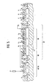
- FIGS. 1a and 1b schematically show a gripped section of a structure in conventional "mixing technology" without claiming to scale accuracy.
- FIG. 1a is the top view
- FIG. 1b is the sectional view identified in FIG. 1a
- FIG. 1c shows the electrical equivalent images of the structures shown in FIGS. 1a and 1b - on the left an I 2 L gate, on the right a bipolar vertical transistor (here of the npn type ).
- mixed media means that both the bipolar components (here vertical npn transistor), which are primarily suitable for analog circuits, and the I 2 L or I 3 L gates, which are suitable for digital circuits, are monolithically integrated on the same chip.
- bipolar components here vertical npn transistor
- I 2 L or I 3 L gates which are suitable for digital circuits
- mixed technology one usually starts from a manufacturing process that satisfies the more extensive and technically more difficult requirements for the properties of the analog components, and tries to meet the requirements with minimal process variants that do not adversely affect the properties of the analog components Properties of the digital gates. Numerous proposals for such process variants have become known in the literature, but only a few of them are currently on the way to technical and economic importance.
- I 2 L technology is also becoming increasingly important in the LSI area because the manufacturing processes are no longer subject to the extremely restrictive requirements for the analog elements and the process results can thus be optimized solely for the I 2 L properties .
- the invention brings a significant improvement in the effective gate current gain.
- the other advantages according to the invention are: improved gate speed and a largely prepared wiring system, the general disadvantages in this regard overcoming I 2 L and I 3 L circuits and preparing the wiring for the use of automatic design systems.
- FIG. 1b The sectional view of a typical mixed technology structure is shown schematically in FIG. 1b.
- a weakly n-doped layer 4 is applied epitaxially to a p-substrate 1 after pre-loading and prediffusion of later "buried" n + regions 2, 3.
- the active chip area is divided into epitaxial "wells" in such a way that the analog components - on the right in FIG. 1a and FIG. 1b - in essentially each individually and the I 2 L or I 3 L gates - on the left in FIG. 1a and FIG. 1b - come to lie in a tub as a whole.
- the n + diffusions 6 establish the electrical connection of the buried layers 2 and 3 to the semiconductor surface and provide in the I 2 L or .
- I 3 L part additionally for electrical shielding of the gates against each other.
- the n + flat diffusion 9 is sometimes used for shielding the gates from one another instead of the n deep diffusion 6 for reasons of space.
- the p-diffusions 7 form, among other things, the base zones for the current-amplifying transistors both in the analog part and in the I 2 L or I 3 L part.
- the injector zones 8 of the digital part also arise in the same diffusion step.
- the flat n + zones 9 are created, the emitter zones in the analog part the vertically downward working npn transistors and in the digital part the collector zones of the vertically upward working npn transistors (several collectors per transistor).
- the contact windows for electrical contacting of the individual zones are shown dark in the plan view according to FIG. 1a. Conductor paths have been omitted for reasons of clarity.
- npn transistor emitter - 7: base - 4, 3, 6: collector
- the vertically upwards working npn -Transistor (6, 2, 4: emitter - 7: base - 9: collector) in the digital part only moderate current amplifications (typically 3 to 10 per collector) - to be understood with cheap collector currents, which are different for the two transistors.
- the switching delay time is approximately constant, because here the approximately current-proportional diffusion capacity controls the switching behavior.
- this diffusion capacity is larger because of the minority storage in the high-resistance emitter region 4 than in the gates of the purely digital I 2 L technology built on a low-resistance epitaxial region, so that the. Mixing technology gates are much slower.
- saturation of the injector structure Miniorticianslic be in epitaxial region 4 additionally stored that need to be addressed in the depletion phase partially, which increases the operating time of the 'gate.
- the removal of the part of the diffusion capacity near the injector is hampered by the fact that the injector continuously supplies (increasing amount of) the current.
- the injector structure can no longer be regarded as a current source.
- Their low source voltage (diode forward voltage minus residual voltage) and the base rail resistances provide for an additional resistance-limited charging of the diffusion capacitance, so that the minimum switch-on delay possible with current source operation is not achieved, and finally in the conventional I 2 L or I 3 L structure due to the successive decrease in the injector current in the direction away from the injector, the last collector always switched on last.
- the additional delays from this are sometimes considerable and determine the maximum permissible clock frequency with clocked logic.
- the metallic injector lines IL 1 , IL 2 are difficult to cross due to electrical reasons of signal lines.
- the injectors are arranged in a row as shown, and gate fields are located on both sides of the injector lines, of which the gate fields GF and GF 2 are particularly marked in FIG. Depending on the need, there is a more or less wide wiring field VF between the gate fields.
- the conditions in the GF 2 gate field are shown as they typically occur:
- the gates are often longer than they should be for electrical and functional reasons, because not all available contact locations can be used to make wiring within the gate field easier . This is primarily a result of the gate position flush with the injector line.
- the space not used due to different gate lengths in the gate field cannot be used for other purposes (e.g. wiring tasks of the wiring field VF).
- the gate field GF 2 is shown again in the gate field GF, with only the electrically necessary gate lengths in the gate field GF to be used. An overall not optimal packing density of the gates becomes clear, which is usually due to the comparatively more difficult wiring of the I 2 L or.
- the solution according to the invention is mainly characterized by an electrical feature and by a geometric feature that describes the arrangement of the elements in the lay-out. In their overall sequence, further advantageous electrical and geometric designs are then possible.
- the task of the lateral injection transistors (8: emitter - 4: base - 7: collector) of the conventional I 2 L or I 3 L structures according to FIG. 1 is to ensure that the working currents for the upward-amplifying gate transistors are as uniform as possible in the entire gate field To provide gates. So it is essentially the property of a constant current source, which in the form of the injector arrangement in is integrated into the gate in an apparently space-saving manner. The significant electrical shortcomings of this power source have been described. A current source that is far more electrically suitable for this task is obtained if, instead of the lateral injection transistor incorporated into the gate according to FIG. 1, a lateral transistor 40 that is electrically insulated from the vertically amplifying gate transistor is used as the current source (FIG. 5).
- FIGS. 4 and 2 The electrical advantages of the freely available base potential at the lateral current source transistor 40 can be seen from FIGS. 4 and 2.
- the base potential of this transistor 40 is initially set only sufficiently far above the reference potential by a voltage source 10, so that the mode of operation of the power supply for an overall circuit designed in this way does not differ from that Operating mode of the power supply of conventional I 2 L or I 3 L circuits would differentiate.
- the electrical sequence can be seen on the basis of the output characteristic of the lateral current source transistor in FIG. 2.
- the operating points for blocked or conductive gates have been set to points A 'and B' (compared to A and B in conventional technology).
- the current difference between the gate switching states has become negligibly small because the current source transistor 40 no longer has to operate in saturation mode even when the gate is conductive.
- the full current gain of the vertical step-up transistor 80 is thus available as a gate current gain. In conventional technology, the gate current gain would be reduced by approximately the quotient from current at operating point A to current at operating point A.
- the voltage source 10 in FIG. 4a can then be, for example, a diode 103 (FIG. 4d) through which the total base current of the lateral transistor and optionally one or more currents flow from partial collectors.
- the diode can in the simplest way consist of an inverter stage 101 of the gate field with a short circuit between the base and the collector (FIG. 5) or with a short circuit between the base and the collectors (see also FIGS. 4b and 4c or in a simplified representation in FIG. 4d).
- a reference current I o is compared either directly or, as in FIG. 4e, via a current mirror 41 with the current of a partial collector 42 of the lateral current source transistor 40.
- the potential of the node 43 is then set such that the base current amplifier (transistor 44) supplies the lateral current source transistor 40 with just as much base current that the current from the sub-collector 42 and thus also the currents from all other similar sub-collectors are just equal to the reference current I o is.
- the current ratio 41 is given a transmission ratio that deviates from 1: 1, then a current translation can also be generated between the reference current I 0 and the current from the partial collector 42.
- the current mirror 41 can again consist of inverter stages of the gate field, it also being possible to make the transmission ratio of the current mirror dependent on the current gain of the gate transistors by means of a base current amplifier 45 according to FIG. 4f.
- the exemplary embodiments according to FIGS. 4g and 4h differ from those according to FIGS. 4e and 4f in that the transistors 44 acting as base current amplifiers are omitted and in each case replaced by a short-circuit line which forms the base of the lateral current source transistor 40 with its sub-collector 42 at the node 43 connects.
- a single, vertically upward-amplifying transistor 900 with at least two collectors is used as the current mirror instead of the current mirror circuits comprising two or three transistors contained in FIGS. 4e and 4f, one (FIG. 4i) or a first interconnected group (FIG.
- the vertically upward amplifying transistor 900 can consist of a gate transistor of a gate array GF.
- Logic circuits according to the invention are largely insensitive to such voltage drops.
- the construction of the power sources provides for all gates approximately the same work flows under all practical operating conditions.
- the current sources are so high from the outset that the opening voltages for the gate transistors (vertical step-up transistors) are always reached. Additional voltage drops between the current source (partial collector) and the base of the gate transistor - for example caused by connecting n-bridges (46 in FIG. 4e) or the base path resistance of the gate transistor itself - can be permitted because there is sufficient voltage space available from the collector of the current source transistor 40 ( not so with a conventional injector). If, on the other hand, one assumes for the blocking case that the reference potential of a gate to be blocked is approximately 200 mV lower than the reference potential of the blocking gate located far away due to voltage drops on the buried layer 2 (FIG.
- the operating current is always fed to the gate via its base contact and is always intercepted at the base contact by a blocking gate, so that the locked gate is completely de-energized.
- the constant current supplying injector of conventional type is removed from the gate so that the barrier obstruction of the gate collectors close to the injector is eliminated.
- the minority-saturated injector volume of the gate is no longer available, so that the blocking delay caused thereby is eliminated.
- the resistance-limited (base rail resistance) charge of the diffusion capacities is eliminated because there is sufficient forward voltage available from the current source.
- the supply of the working current takes place conventionally from the electrically least favorable position on the narrow side of the elongated gate strip (FIG. 3). According to the invention, there is always a more favorable position for the supply via the base contact B i (FIG. 5).
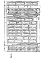
- FIG. 6 shows a simplified lay-out of a four-stage asynchronous frequency divider.
- the contact windows are marked with dots.
- the boundary lines of the gate collectors (emitter diffusion) in the gate strip and the conductor tracks have not been drawn in for the sake of clarity.
- Figure 7 shows the formal lay-out of the frequency divider stage. It shows the gate strips with their collector connections (x) and their base connections (o) as well as the conductive connections made of metal or polycrystalline semiconductor material (solid lines) and the bridges made of low-resistance, diffused semiconductor material (dashed lines).
- the one from the Gate fields at the top and bottom of the conductor tracks each lead to a partial collector of the lateral current source transistors 40.
- the current source transistors are electrically isolated lateral transistors and are therefore always completely enclosed by areas of insulation diffusion 51.
- the elongated emitter 52 of the transistor consisting of base diffusion material, is generally in the center line of the transistor.
- collectors 53 On both sides of the emitter 52 there is a large number of collectors 53, likewise made of material of the basic diffusion, to which the individual working currents for the gate field GF, driver stages and reference circuits are removed.
- At least one base connection 55 must be available for each current source transistor SQ.
- the electrical transistor base 54 is formed by the epitaxial material between the emitter 52 and the individual collectors 53. Their consistently good electrical contact to the base connection 55 determines the achievable uniformity of all collector currents.
- the gate field GF is therefore expediently constructed in a first rough structure from columns perpendicular to the longitudinal direction of the current source transistors SQ, the width of which is alternately dimensioned for three and four contact locations, the location for the (shielding) deep collector diffusion 58 (zone 6 in the 1 L part of FIGS. 1a and 1b). Circuitry and lay-out requirements then force one to break this rigid scheme: gates with different numbers of collector positions have to be inserted, and the rigid column formation almost never fits into the considerations of a sensible lay-out.
- Wiring in the gate field is only possible via a contact location of the gate for gate-crossing interconnects (conventionally the same way); the gap between the gates is available for gate-passing interconnects.
- two conductor tracks can be routed in parallel, both vertically and horizontally. In principle, this is also possible in a conventional manner, but because of the different type of gate arrangement, there is virtually no use of two parallel conductor tracks between the gates.
- These wiring options can be used in the arrangement of the gates according to the invention. Experience has shown that this gives the lay-out more than just the freedom required to attach the additional conductor tracks for the working currents from current source transistors.
- the wiring space is sufficient to be able to arrange up to ten gate rows between two current source transistors. This means that a D - flip-flop with six to nine gates (as the most important large cell) can be arranged in a column between two current source transistors.
- the wiring fields VF lie between the gate field GF and the current source transistor or the current source transistors. All working currents must be routed into the gate field GF via the wiring fields VF. However, this means that all logical signals are available in the wiring fields VF, because the potentials of the work Electricity traces are the logical signals. This is the task of the wiring fields: decoupling logical signals and crossing signal lines if this cannot be achieved in the wiring of the gate field.
- the conductor tracks of the wiring field VF are the bridges 59 made of material of the emitter diffusion. They lie in an oppositely doped region 60 made of base diffusion material which overlaps for electrical contacting with the region 51 which borders the current source transistor SQ.
- the total area required for the solution according to the invention is initially burdened by the additional, fully insulated current source transistors SQ.
- the omission of the injectors in the gate fields only partially compensates for this additional effort.
- the more expedient arrangement of the gate field and thus inextricably linked the systematization of the wiring problem and the greater freedom for this in the gate field give an overall area advantage for circuits which contain more than about 80 gates.
- the invention is not limited to the exemplary embodiments described with reference to the drawing.
- the inverse structures and circuits in which the p-type zones are replaced by n-type zones and vice versa are also conceivable.
Landscapes
- Engineering & Computer Science (AREA)
- Power Engineering (AREA)
- Physics & Mathematics (AREA)
- Computer Hardware Design (AREA)
- Computing Systems (AREA)
- General Engineering & Computer Science (AREA)
- Mathematical Physics (AREA)
- Bipolar Integrated Circuits (AREA)
Abstract
Description
Die Erfindung geht aus von einer bipolar integrierten Inverstransistorlogik nach der Gattung des Hauptanspruchs.The invention is based on a bipolar integrated transistor transistor logic according to the type of the main claim.
Aus dem "Fairchild Journal of Semiconductor Progress", Band 8, Nr. 2 (März/April 1980) ist bereits eine Inverstransistorlogik - im folgenden kurz mit ITL bezeichnet - dieser Art bekannt, bei der die Basis des lateralen Stromquellentransistors und der Emitter des Gattertransistors auf dasselbe Potential (Massepotential) gelegt sind, womit auch der im Betrieb der Gatter auftretende Sättigungszustand des Injektorteils (hier separater Lateraltransistor) in I2L-üblicher Weise unvermeidbar und mit allen Nachteilen auf das Gatterverhalten bestehen bleibt. Immerhin ist die örtliche Trennung von Injektorteil und Verstärkertransistor vollzogen, was man im Sinne der merged transistor logic eigentlich immer als einen Nachteil bezüglich Flächenaufwand verstanden hat. Damit entfällt eigentlich auch schon die Berechtigung für die Bezeichnung "Injektionslogik", denn der direkt in die Basis des Verstärkertransistors injizierte Ansteuerstrom existiert als solcher nicht mehr. Er ist ersetzt durch einen Ansteuerstrom, der einem körperlich vorhandenen separaten Lateralkollektor eines Stromquellentransistors entnommen wird und über eine metallisch leitende Verbindung der Basis des Verstärkertransistors zugeführt wird.From the "Fairchild Journal of Semiconductor Progress",
Die erfindungsgemäße bipolar integrierte Inverstransistorlogik mit den kennzeichnenden Merkmalen des Hauptanspruchs hat demgegenüber den Vorteil, daß das Basispotential des lateralen'Stromquellentransistors frei wählbar ist. Gemäß Anspruch 2 kann das Basispotential des lateralen Stromquellentransistors so eingestellt werden, daß dieser Transistor auch bei leitendem Gatter nicht mehr im Sättigungsbetrieb arbeitet, so daß damit die volle Stromverstärkung des vertikal aufwärts verstärkenden Gattertransistors als Gatterstromverstärkung zur Vefügung steht. Wenn der laterale Stromquellentransistor vom pnp-Typ und der Gattertransistor vom npn-Typ ist, so muß hierzu das Basispotential des Stromquellentransistors über das Emitterpotential des Gattertransistors angehoben werden. Ist dagegen der laterale Stromquellentransistor vom npn-Typ und der Gattertransistor vom pnp-Typ, so muß das Basispotential des Stromquellentransistors unter das Emitterpotential des Gattertransistors abgesenkt werden. Sind mehrere Gattertransistoren vorhanden, so können diese aus einem einzigen Stromquellentransistor, der mit mehreren Kollektoren versehen ist, mit Arbeitsströmen versorgt werden. Der Stromquellentransistor liefert dann für alle Gattertransistoren unter allen praktischen Betriebsbedingungen etwa gleiche Arbeitsströme. Die Sättigungspotentiale an den Kollektoren dieser Stromquellentransistoren liegen dann gegenüber dem Gatter-Bezugspotential so hoch, daß die Öffnungsspannungen für die Gattertransistoren immer erreicht werden. Weitere Vorteile ergeben sich aus den weiteren Unteransprüchen 3 bis 31 und aus der Beschreibung.The bipolar integrated inverter transistor logic according to the invention with the characterizing features of the main claim has the advantage that the base potential of the lateral current source transistor is freely selectable. According to
Ausführungsbeispiele der erfindungsgemäßen bipolar integrierten Inverstransistorlogik sind in der Zeichnung dargestellt und in der nachfolgenden Beschreibung näher erläutert. Es zeigen:
- Figur 1a eine Draufsicht auf eine bekannte I3L-Struktur in schematischer Darstellung,
- Figur 1b einen Schnitt nach der Linie AB der Figur 1a,
- Figur 1c die elektrischen Ersatzbilder des I2L-Teils und des Analogteils der in den Figuren 1a und 1b dargestellten I3L-Struktur,
Figur 2 die Ausgangskennlinie des lateralen pnp-Injektionstransistors der bekannten I2L-Struktur bzw. die Ausgangskennlinie des lateralen Stromquellentransistors der erfindungsgemäßen ITL-Struktur,Figur 3 eine schematisierte Draufsicht auf ein lay-out einer bekannten I2L- bzw. I3L-Schaltung,- Figur 4a das elektrische Ersatzbild eines ersten Ausführungsbeispiels einer erfindungsgemäßen Inverstransistorlogik, bei dem das Basispotential des lateralen pnp-Stromquellentransistors durch eine Spannungsquelle hinreichend weit über dem Bezugspotential festgelegt ist,
- Figur 4b die Schaltung nach Figur 4a, bei der die Spannungsquelle durch einen npn-Transistor mit Kurzschluß zwischen Basis und Kollektor gebildet ist,
- Figur 4c die Schaltung nach Figur 4b, jedoch mit zwei npn-Gattertransistoren und mit einem mit drei Kollektoren versehenen lateralen pnp-Stromquellentransistor, wobei zwei dieser Kollektoren die Arbeitsströme für die beiden Gattertransistoren liefern und der dritte dieser Kollektoren an die kurzgeschlossene Basis-Kollektor-Strecke des als Spannungsquelle dienenden npn-Transistors angeschlossen ist,
- Figur 4d die Schaltung nach Figur 4c in vereinfachter symbolischer Darstellung,
- Figur 4e das elektrische Ersatzbild eines weiteren, besonders vorteilhaften Ausführungsbeispiels einer erfindungsgemäßen Inverstransistorlogik,
- Figur 4f eine Schaltung ähnlich der der Figur 4e,
- Figur 4g bis 4k weitere Schaltungsvarianten ähnlich denjenigen der Figuren 4e und 4f,
Figur 5 das Ausführungsbeispiel nach Figur 4b zusammen mit einem sich daran anschließenden Analogteil im Schnitt,Figur 6 ein vereinfachtes lay-out eines vierstufigen asynchronen Frequenzteilers,- Figur 7 das formale lay-out der
Frequenzteilerstufe nach Figur 6.
- FIG. 1a shows a schematic top view of a known I 3 L structure,
- 1b shows a section along the line AB of FIG. 1a,
- 1c shows the electrical equivalent images of the I 2 L part and the analog part of the I 3 L structure shown in FIGS. 1a and 1b,
- FIG. 2 shows the output characteristic of the lateral pnp injection transistor of the known I 2 L structure or the output characteristic of the lateral current source transistor of the ITL structure according to the invention,
- FIG. 3 shows a schematic plan view of a lay-out of a known I 2 L or I 3 L circuit,
- FIG. 4a shows the electrical equivalent image of a first exemplary embodiment of an invert transistor logic according to the invention, in which the base potential of the lateral pnp current source transistor is set sufficiently far above the reference potential by a voltage source,
- 4b shows the circuit according to FIG. 4a, in which the voltage source is formed by an npn transistor with a short circuit between the base and the collector,
- 4c shows the circuit according to FIG. 4b, but with two npn gate transistors and with a lateral pnp current source transistor provided with three collectors, two of these collectors supplying the working currents for the two gate transistors and the third of these collectors to the short-circuited base-collector path the npn transistor serving as voltage source is connected,
- FIG. 4d shows the circuit according to FIG. 4c in a simplified symbolic representation,
- FIG. 4e shows the electrical equivalent image of a further, particularly advantageous exemplary embodiment of an invert transistor logic according to the invention,
- FIG. 4f shows a circuit similar to that of FIG. 4e,
- 4g to 4k further circuit variants similar to those of FIGS. 4e and 4f,
- 5 shows the exemplary embodiment according to FIG. 4b together with an adjoining analog part in section,
- FIG. 6 shows a simplified lay-out of a four-stage asynchronous frequency divider,
- FIG. 7 the formal lay-out of the frequency divider stage according to FIG. 6.
Die Figuren 1a und 1b zeigen schematisiert und ohne Anspruch auf maßstäbliche Genauigkeit einen gegriffenen Ausschnitt einer Struktur in konventioneller "Mischtechnik". Figur 1a ist die Draufsicht, Figur 1b ist die in Figur 1a gekennzeichnete Schnittansicht, Figur 1c zeigt die elektrischen Ersatzbilder der in den Figuren 1a und 1b dargestellten Strukturen - links ein I2L-Gatter, rechts einen bipolaren Vertikaltransistor (hier vom npn-Typ).FIGS. 1a and 1b schematically show a gripped section of a structure in conventional "mixing technology" without claiming to scale accuracy. FIG. 1a is the top view, FIG. 1b is the sectional view identified in FIG. 1a, FIG. 1c shows the electrical equivalent images of the structures shown in FIGS. 1a and 1b - on the left an I 2 L gate, on the right a bipolar vertical transistor (here of the npn type ).
Der Begriff "Mischtechnik" sagt aus, daß auf demselben Chip sowohl die vorwiegend für analoge Schaltungen geeigneten bipolaren Bauelemente (hier vertikaler npn-Transistor) als auch die für digitale Schaltungen geeigneten I2L- bzw. I3L-Gatter monolithisch integriert vorkommen. Bei der-Mischtechnik geht man meist von einem Herstellungsprozeß aus, der die umfangreicheren und technisch schwierigeren Anforderungen an die Eigenschaften der Analog-Bauelemente befriedigt, und versucht, mit möglichst geringfügigen und die Eigenschaften der Analog-Bauelemente nicht negativ beeinflussenden Prozeßvarianten auch die Anforderungen an die Eigen- - schaften der digitalen Gatter zu erfüllen. In der Literatur sind zahlreiche Vorschläge für solche Prozeßvarianten bekanntgeworden, von denen aber zur Zeit nur sehr wenige auf dem Wege zu technisch-wirtschaftlicher Bedeutung sind. Für reine-Digitalanwendungen gewinnt die I2L-Technik zunehmend auch im LSI-Bereich an Bedeutung, weil bezüglich der Herstellungsprozesse die stark einschränkenden Forderungen für die Analog-Elemente hier entfallen und man damit die Prozeßergebnisse allein auf die I2L-Eigenschaften optimieren kann.The term "mixed media" means that both the bipolar components (here vertical npn transistor), which are primarily suitable for analog circuits, and the I 2 L or I 3 L gates, which are suitable for digital circuits, are monolithically integrated on the same chip. In mixed technology, one usually starts from a manufacturing process that satisfies the more extensive and technically more difficult requirements for the properties of the analog components, and tries to meet the requirements with minimal process variants that do not adversely affect the properties of the analog components Properties of the digital gates. Numerous proposals for such process variants have become known in the literature, but only a few of them are currently on the way to technical and economic importance. For purely digital applications, I 2 L technology is also becoming increasingly important in the LSI area because the manufacturing processes are no longer subject to the extremely restrictive requirements for the analog elements and the process results can thus be optimized solely for the I 2 L properties .
Die Beschreibung von Struktur und elektrischem Verhalten erfolgt anhand der Mischtechnik-Struktur der Figur 1.The structure and electrical behavior are described using the mixed technology structure of FIG. 1.
Die Erfindung bringt eine erhebliche Verbesserung der effektiven Gatterstromverstärkung. Die übrigen erfindungsgemäßen Vorteile sind: Verbesserte Gattergeschwindigkeit und ein weitgehend vorbereitetes Verdrahtungssystem, das diesbezügliche allgemeine Nachteile von I2L- und I3L-Schaltungen überwindet und die Verdrahtung für die Anwendung automatischer Entwurfsanlagen aufbereitet.The invention brings a significant improvement in the effective gate current gain. The other advantages according to the invention are: improved gate speed and a largely prepared wiring system, the general disadvantages in this regard overcoming I 2 L and I 3 L circuits and preparing the wiring for the use of automatic design systems.
In Figur 1b ist das Schnittbild einer typischen Mischtechnik-Struktur schematisch dargestellt. Auf einem p-Substrat 1 wird nach Vorbelegung und Vordiffusion von später "vergrabenen" n+-Gebieten 2, 3 eine schwach n-dotierte Schicht 4 epitaktisch aufgebracht. Mit den p -Diffusionen 5, die die elektrische Kontaktierung des p-Substrats 1 von der Halbleiteroberfläche her ermöglichen, wird die aktive Chipfläche so in Epitaxie-"Wannen" aufgeteilt, daß die Analog-Bauelemente - rechts in Figur 1a und Figur 1b - im wesentlichen je einzeln und die I2L- bzw. I3L-Gatter - links in Figur 1a und Figur 1b - insgesamt in eine Wanne zu liegen kommen. Die n+-Diffusionen 6 stellen die elektrische Verbindung der vergrabenen Schichten 2 und 3 zur Halbleiteroberfläche her und sorgen im I2L- bzw. I3L-Teil zusätzlich für die elektrische Abschirmung der Gatter gegeneinander. Im I2L- bzw. I3L-Teil wird zur Abschirmung der Gatter gegeneinander anstelle der n - Tiefdiffusion 6 mitunter aus Platzgründen die n+-Flachdiffusion 9 verwendet. Die p-Diffusionen 7 bilden unter anderem sowohl im Analogteil als auch I2L- bzw. I3L-Teil die Basiszonen für die stromverstärkenden Transistoren. Im gleichen Diffusionsschritt entstehen auch die Injektorzonen 8 des Digitalteils. Im letzten Diffusionsschritt entstehen die flachen n+-Zonen 9, die im Analogteil die Emitterzonen der vertikal abwärts arbeitenden npn-Transistoren und im Digitalteil die Kollektorzonen der vertikal aufwärts arbeitenden npn-Transistoren (mehrere Kollektoren pro Transistor) bilden. Die Kontaktfenster zur elektrischen Kontaktierung der einzelnen Zonen sind in der Draufsicht nach Figur 1a dunkel dargestellt. Auf Darstellung von Leiterbahnen wurde mit Rücksicht auf Übersichtlichkeit verzichtet.The sectional view of a typical mixed technology structure is shown schematically in FIG. 1b. A weakly n-doped layer 4 is applied epitaxially to a p-substrate 1 after pre-loading and prediffusion of later "buried" n + regions 2, 3. With the p -
Während der im Analogteil vertikal abwärts arbeitende npn-Transistor (9:Emitter - 7:Basis - 4, 3, 6:Kollektor) durch den so gewollten Aufbau der Struktur gute Stromverstärkung zeigt (typisch 100 bis 200), erreicht der vertikal aufwärts arbeitende npn-Transistor (6, 2, 4: Emitter - 7:Basis - 9:Kollektor) im Digitalteil nur mäßige Stromverstärkungen (typisch 3 bis 10 pro Kollektor) - zu verstehen bei jeweils,günstigen Kollektorströmen, die für die beiden Transistoren unterschiedlich sind. Die Situation verschärft sich für den Aufwärtstransistor noch durch die Art seiner Ansteuerung über die laterale pnp-Injektionsstruktur (8:Emitter - 4:Basis - 7:Kollektor = Basis des Aufwärtstransistors). Dem elektrischen Ersatzbild des Gatters - Figur 1c links - entnimmt man sofort, daß der pnp-Injektionstransistor sättigt, sobald er den Aufwärtstransistor leitend steuert, der Injektionsstrom also nicht über den Basiskontakt B. und einen leitenden-Kollektor eines zweiten Gatters extern abgeleitet wird. Das bedeutet aber, daß der Ansteuerstrom für den Aufwärtstransistor durch die sättigende Injektionsstruktur gerade dann verringert wird, wenn der Aufwärtstransistor diesen Strom zum Aufrechterhalten seines Leitungszustandes benötigt, und andererseits im Sperrzustand das sperrende Gatter mit dem vollen Injektionsstrom belastet wird, weil die Injektionsstruktur sich in diesem Fall nicht im Sättigungszustand befindet.While the npn transistor (9: emitter - 7: base - 4, 3, 6: collector) working vertically downwards in the analog section shows good current amplification (typically 100 to 200) due to the desired structure, the vertically upwards working npn -Transistor (6, 2, 4: emitter - 7: base - 9: collector) in the digital part only moderate current amplifications (typically 3 to 10 per collector) - to be understood with cheap collector currents, which are different for the two transistors. The situation is aggravated for the step-up transistor by the way it is controlled via the lateral pnp injection structure (8: emitter - 4: base - 7: collector = base of the step-up transistor). The electrical equivalent image of the gate - FIG. 1c on the left - shows immediately that the pnp injection transistor saturates as soon as it controls the step-up transistor so that the injection current is not externally derived via the base contact B. and a conductive collector of a second gate. However, this means that the drive current for the step-up transistor is reduced by the saturating injection structure just when the step-up transistor sistor needs this current to maintain its conduction state, and on the other hand the blocking gate is loaded with the full injection current in the blocking state, because in this case the injection structure is not in the saturation state.
In Figur 2 sind diese Verhältnisse anhand der beiden Arbeitspunkte A (gesättigt, leitender Aufwärtstransistor) und B (nicht gesättigt, gesperrter Aufwärtstransistor) in der Ausgangskennlinie des lateralen Injektionstransistors anschaulich dargestellt. Diese Verhältnisse führen unmittelbar auf die Formulierung einer effektiven Stromverstärkung für das Gesamtgatter. Werte hierfür liegen für die Mischtechnik so risikoreich niedrig, daß sich die Anwendung dieser Technik nicht selten verbietet. Problemlösungen wurden bisher im technologischen Bereich durch Prozeßvarianten für die Wafer-Herstellung gesucht, z.B. DE-OS 28 35 330. Die Erfindung bietet eine Lösung auf der Ebene der Schaltungstechnik an.In Figure 2, these relationships are clearly shown using the two operating points A (saturated, conductive step-up transistor) and B (unsaturated, blocked step-up transistor) in the output characteristic of the lateral injection transistor. These relationships lead directly to the formulation of an effective current gain for the entire gate. Values for this are so low for the mixing technology that the use of this technology is often prohibited. So far, solutions to problems have been sought in the technological area through process variants for wafer production, e.g. DE-OS 28 35 330. The invention offers a solution at the level of circuit technology.
Im Bereich maximaler Schaltgeschwindigkeit der Gatter ist die-Schaltverzögerungszeit annähernd konstant, weil hier die etwa stromproportionale Diffusionskapazität das Schaltverhalten beherrscht. In der Mischtechnik ist diese Diffusionskapazität aufgrund der Minioritätenspeicherung im hochohmigen Emittergebiet 4 größer als bei den auf niederohmigem Epitaxiegebiet aufgebauten Gattern der rein digitalen I2L-Technik, so daß die . Gatter der Mischtechnik sehr viel langsamer sind. Bei detaillierterer Betrachtung muß man die Einflüsse der gesättigten Injektorstruktur, der Basis-Bahnwiderstände und des abnehmenden Injektorstromes in Richtung vom Injektor weg mit berücksichtigen. Bei Sättigung der Injektorstruktur werden im Epitaxiegebiet 4 zusätzlich Minioritätsträger gespeichert, die in der Ausräumphase zum Teil mit ausgeräumt werden müssen, was die Ausschaltzeit des'Gatters vergrößert. Weiterhin ist das AuSräumen des injektornahen Teils der Diffusionskapazität (betreffend C1 und C2 in Figur lb) dadurch behindert, daß der Injektor ständig (im Ausräumen zunehmend) Strom nachliefert.In the range of the maximum switching speed of the gates, the switching delay time is approximately constant, because here the approximately current-proportional diffusion capacity controls the switching behavior. In the mixed technology, this diffusion capacity is larger because of the minority storage in the high-resistance emitter region 4 than in the gates of the purely digital I 2 L technology built on a low-resistance epitaxial region, so that the. Mixing technology gates are much slower. At In more detail, one has to take into account the influences of the saturated injector structure, the basic path resistances and the decreasing injector current in the direction away from the injector. When saturation of the injector structure Minioritätsträger be in epitaxial region 4 additionally stored that need to be addressed in the depletion phase partially, which increases the operating time of the 'gate. Furthermore, the removal of the part of the diffusion capacity near the injector (regarding C 1 and C 2 in FIG. 1b) is hampered by the fact that the injector continuously supplies (increasing amount of) the current.
Bei höheren Injektorströmen (Bereich hoher Schaltgeschwindigkeit) kann die Injektorstruktur nicht mehr als Stromquelle betrachtet werden. Ihre niedrige Quellenspannung (Dioden-Flußspannung abzüglich Restspannung) und die Basis-Bahnwiderstände sorgen für;eine zusätzlich widerstandsbegrenzte Aufladung der Diffusionskapazität, so daß die bei Stromquellenbetrieb minimal mögliche Einschaltverzögerung nicht erreicht wird, und schließlich wird in der konventionellen I2L- bzw. I3L-Struktur infolge der sukzessiven Abnahme des Injektorstromes in Richtung vom Injektor weg der letzte Kollektor immer zuletzt eingeschaltet. Die Zusatzverzögerungen hieraus sind zum Teil erheblich und bestimmen bei getakteter Logik die höchstzulässige Taktfrequenz. Diese Nachteile werden durch die Erfindung zum Teil beseitigt, zum Teil gemildert.At higher injector currents (high switching speed range), the injector structure can no longer be regarded as a current source. Their low source voltage (diode forward voltage minus residual voltage) and the base rail resistances provide for an additional resistance-limited charging of the diffusion capacitance, so that the minimum switch-on delay possible with current source operation is not achieved, and finally in the conventional I 2 L or I 3 L structure due to the successive decrease in the injector current in the direction away from the injector, the last collector always switched on last. The additional delays from this are sometimes considerable and determine the maximum permissible clock frequency with clocked logic. These disadvantages are partly eliminated and partly alleviated by the invention.
In Figur 3 sind die Layoutverhältnisse konventioneller I2L- bzw. I3L-Schaltungen schematisiert in der Draufsicht dargestellt. Die Kontaktfenster sind durch Punkte symbolisiert. Vom Gatteraufbau sind nur die Umrisse der schirmenden n+-Tiefdiffusion 6, die Umrisse der Injektorgebiete 8 und die Umrisse der Basisgebiete der Aufwärtstransistoren 7 gezeichnet.In Figure 3, the layout ratios of conventional I 2 L or . I 3 L circuits schematized in plan view shown. The contact windows are symbolized by dots. From the gate structure, only the outlines of the shielding n +
Die metallischen Injektorlinien IL1, IL2 sind aus elektrischen Gründen von Signalleitungen nur schwer zu kreuzen. Die Injektoren werden wie dargestellt in Reihe angeordnet, und zu beiden Seiten der Injektorlinien liegen Gatterfelder, von denen in Figur 3 die Gatterfelder GF und GF2 besonders gekennzeichnet sind. Zwischen den Gatterfeldern liegt je nach Notwendigkeit ein mehr oder minder breites Verdrahtungsfeld VF.The metallic injector lines IL 1 , IL 2 are difficult to cross due to electrical reasons of signal lines. The injectors are arranged in a row as shown, and gate fields are located on both sides of the injector lines, of which the gate fields GF and GF 2 are particularly marked in FIG. Depending on the need, there is a more or less wide wiring field VF between the gate fields.
Im Gatterfeld GF2 sind die Verhältnisse dargestellt, wie sie typisch auftreten: Die Gatter sind häufig länger, als sie aus elektrisch-funktionellen Gründen sein müßten, weil nicht alle zur Verfügung stehenden Kontaktplätze genutzt werden können, um so die Verdrahtung innerhalb des Gatterfeldes zu erleichtern. Dies ist vorwiegend eine Folge der an der Injektorlinie bündigen Gatterlage. Der aufgrund unterschiedlicher Gatterlängen im Gatterfeld nicht genutzte Platz ist für andere Zwecke (z.B. Verdrahtungsaufgaben des Verdrahtungsfeldes VF) nicht nutzbar. Um eine Vorstellung davon zu vermitteln, wieviel Fläche durch die Kontakt-Leerplätze einschließlich unterschiedlicher Gatterlänge insgesamt verloren geht, ist das Gatterfeld GF2 im Gatterfeld GF erneut dargestellt, wobei im Gatterfeld GF nur die elektrisch notwendigen Gatterlängen benutzt werden. Es wird eine insgesamt nicht optimale Packungsdichte der Gatter deutlich, die gewöhnlich der vergleichsweise schwierigeren Verdrahtung der I2L-bzw. I3L-Technik angelastet wird. Zweifellos entstehen durch die schwer kreuzbaren Injektorlinien und das dicht verdrahtete Gatterfeld, aus dem man.zusätzlich die logischen Signale herausführen muß, für die Verdrahtung Zwänge, die anderen LSI-Techniken nicht in dem Maße eigen sind. Auch eine Zweilagenverdrahtung löst das Problem nur zum geringen Teil. Man erreicht dann zwar die Form des Gatterfeldes GF1" darf aber nicht erwarten, daß die gegenüberliegenden Gatterfelder so ineinanderzahnen, daß die Lücken aufgrund unterschiedlicher Gatterlänge verschwinden. Sie bleiben zum größten Teil bestehen.The conditions in the GF 2 gate field are shown as they typically occur: The gates are often longer than they should be for electrical and functional reasons, because not all available contact locations can be used to make wiring within the gate field easier . This is primarily a result of the gate position flush with the injector line. The space not used due to different gate lengths in the gate field cannot be used for other purposes (e.g. wiring tasks of the wiring field VF). In order to convey an idea of how much area is lost overall through the contact vacancies, including different gate lengths, the gate field GF 2 is shown again in the gate field GF, with only the electrically necessary gate lengths in the gate field GF to be used. An overall not optimal packing density of the gates becomes clear, which is usually due to the comparatively more difficult wiring of the I 2 L or. I 3 L technology is loaded. Undoubtedly, the injector lines, which are difficult to cross, and the densely wired gate field, from which the logical signals also have to be brought out, create constraints for the wiring that are not so characteristic of other LSI techniques. Even two-layer wiring only partially solves the problem. Although the shape of the gate field GF 1 " is then reached, one must not expect the opposite gate fields to interlock so that the gaps disappear due to different gate lengths. They remain for the most part.
Die erfindungsgemäße Lösung kennzeichnet sich hauptsächlich durch ein elektrisches Merkmal und durch ein geometrisches, die Anordnung der Elemente im lay-out beschreibendes Merkmal. In deren Gesamtfolge sind dann weitere vorteilhafte Ausbildungen elektrischer und geometrischer Art möglich.The solution according to the invention is mainly characterized by an electrical feature and by a geometric feature that describes the arrangement of the elements in the lay-out. In their overall sequence, further advantageous electrical and geometric designs are then possible.
Die Aufgabe der lateralen Injektionstransistoren (8: Emitter - 4:Basis - 7:Kollektor) der konventionellen I 2L- bzw. I3L-Strukturen nach Figur 1 ist es, die Arbeitsströme für die aufwärts verstärkenden Gattertransistoren im gesamten Gatterfeld möglichst gleichmäßig pro Gatter zur Verfügung zu stellen. Es ist also im wesentlichen die Eigenschaft einer Konstantstromquelle, die in Form der Injektoranordnung in scheinbar platzsparender Weise in das Gatter einintegriert wird. Die erheblichen elektrischen Mängel dieser Stromquelle wurden beschrieben. Eine elektrisch für diese Aufgabe weitaus besser geeignete Stromquelle erhält man, wenn anstelle des gemäß Figur 1 in das Gatter einbezogenen lateralen Injektionstransistors ein vom vertikal aufwärts verstärkenden Gattertransistor elektrisch isolierter lateraler Transistor 40 als Stromquelle verwendet wird (Figur 5). Die wesentliche Folge ist, daß das Basispotential dieses vollisolierten Transistors 40 nicht mehr wie in der konventionellen I2L- bzw. I3L-Struktur zwangsweise auf dem Bezugspotential des Gatters liegt, sondern im Gegensatz dazu frei wählbar ist. Darin liegt auch der wesentliche Unterschied zu der im "Fairchild Journal of Semiconductor Progress", Band 8, Nr. 2 angegebenen Struktur: Die örtliche Trennung von Injektorstruktur und vertikal aufwärts verstärkendem Gattertransistor ist dort bereits vollzogen, aber im Gegensatz zur erfindungsgemäßen Lösung bleibt die elektrische Verbindung des Basispotentials des Injektionstransistors mit dem Gatter-Bezugspotential dort bestehen.The task of the lateral injection transistors (8: emitter - 4: base - 7: collector) of the conventional I 2 L or I 3 L structures according to FIG. 1 is to ensure that the working currents for the upward-amplifying gate transistors are as uniform as possible in the entire gate field To provide gates. So it is essentially the property of a constant current source, which in the form of the injector arrangement in is integrated into the gate in an apparently space-saving manner. The significant electrical shortcomings of this power source have been described. A current source that is far more electrically suitable for this task is obtained if, instead of the lateral injection transistor incorporated into the gate according to FIG. 1, a
Die elektrischen Vorteile des frei verfügbaren Basispotentials am lateralen Stromquellentransistor 40 sind anhand von Figur 4 und Figur 2 ersichtlich. In Figur 4a ist das Basispotential dieses Transistors 40 zunächst nur durch eine Spannungsquelle 10 hinreichend weit über dem Bezugspotential festgelegt, so daß sich im übrigen die Betriebsweise der Stromversorgung für eine so konzipierte Gesamtschaltung nicht von der Betriebsweise der Stromversorgung konventioneller I2L- bzw. I3L-Schaltungen unterscheiden vürde. Die elektrische Folge erkennt man anhand der Ausgangskennlinie des lateralen Stromquellentransistors in Figur 2. Die Arbeitspunkte für gesperrtes bzw. leitendes Gatter haben sich auf die Punkte A' bzw. B' eingestellt (gegenüber A bzw. B bei konventioneller Technik). Die Stromdifferenz zwischen den Gatter-Schaltzuständen ist vernachlässigbar klein geworden, weil der Stromquellentransistor 40 auch bei leitendem Gatter nicht mehr im Sättigungsbetrieb arbeiten muß. Damit steht die volle Stromverstärkung des vertikalen Aufwärtstransistors 80 als Gatterstromverstärkung zur Verfügung. In konventioneller Technik wäre die Gatterstromverstärkung etwa um den Quotienten aus Strom im Arbeitspunkt A zu Strom im Arbeitspunkt A vermindert.The electrical advantages of the freely available base potential at the lateral
In der erfindungsgemäßen Lösung werden alle Injektorströme konventioneller Art durch Ströme aus Stromquellen 40 der beschriebenen Art ersetzt. Da man aus Platzgründen nicht für jeden Arbeitsstrom jeweils einen elektrisch vollständig isolierten Transistor 40 zur Verfügung stellen sollte, baut man diese Stromquellen vorteilhaft mit Hilfe der bekannten Lateraltransistoren mit vielfach unterteiltem Kollektor auf, wie sie auch in Figur 6 (Felder SQ) in der Draufsicht erkennbar sind, so daß jeder Teilkollektor den Arbeitsstrom für jeweils ein Gatter zur Verfügung stellt.In the solution according to the invention, all conventional injector currents are replaced by currents from
Die Spannungsquelle 10 in Figur 4a kann dann z.B. eine Diode 103 (Figur 4d) sein, durch die der Gesamtbasisstrom des Lateraltransistors und gegebenenfalls ein oder mehrere Ströme aus Teilkollektoren fließen. Die Diode kann in einfachster Weise aus einer Inverterstufe 101 des Gatterfeldes mit Kurzschluß zwischen Basis und Kollektor (Figur 5) bzw. mit Kurzschluß zwischen Basis und Kollektoren bestehen (siehe auch Figur 4b und 4c bzw. in vereinfachter Darstellung Figur 4d).The
Im Sinne der Erfindung bietet sich allerdings die weit vorteilhaftere Lösung nach Figur 4e für die Gesamtstromversorgung des Gatterfeldes an. Ein Referenzstrom Io wird entweder direkt oder wie in Figur 4e über einen Stromspiegel 41 mit dem Strom eines Teilkollektors 42 des lateralen Stromquellentransistors 40 verglichen. Das Potential des Knotenpunktes 43 stellt sich dann so ein, daß der Basisstromverstärker (Transistor 44) dem lateralen Stromquellentransistor 40 gerade so viel Basisstrom zuführt, daß der Strom aus dem Teilkollektor 42 und damit auch die Ströme aus allen anderen gleichartigen Teilkollektoren gerade gleich dem Referenzstrom I o ist. Gibt man dem Stromspiegel 41 ein von 1:1 abweichendes Übersetzungsverhältnis, dann kann auch eine Stromübersetzung zwischen dem Referenzstrom Io und dem Strom aus dem Teil- kollektor 42 erzeugt werden. In einfachster Weise kann der Stromspiegel 41 wieder aus Inverterstufen des Gatterfeldes bestehen, wobei man zusätzlich das Übersetzungsverhältnis des Stromspiegels durch einen Basisstromverstärker 45 nach Figur 4f von der Stromverstärkung der Gattertransistoren abhängig machen kann.In the sense of the invention, however, the far more advantageous solution according to FIG. 4e offers itself for the overall power supply of the gate field. A reference current I o is compared either directly or, as in FIG. 4e, via a
Weitere Schaltungsvarianten sind in den Figuren 4g bis 4k dargestellt.Further circuit variants are shown in Figures 4g to 4k.
Die Ausführungsbeispiele nach den Figuren 4g und 4h unterscheiden sich von denjenigen nach den Figuren 4e und 4f dadurch, daß die als Basisstromverstärker wirkenden Transistoren 44 weggelassen und jeweils durch eine Kurzschlußleitung ersetzt sind, die die Basis des lateralen Stromquellentransistors 40 mit seinem Teilkollektor 42 am Knotenpunkt 43 verbindet. Bei den Ausführungsbeispielen nach den Figuren 4i und 4k wird als Stromspiegel anstelle der in den Figuren 4e und 4f enthaltenen, aus zwei bzw. drei Transistoren bestehenden Stromspiegelschaltungen ein einziger, vertikal aufwärts verstärkender Transistor 900 mit mindestens zwei Kollektoren verwendet, wobei einer (Figur 4i) oder eine erste zusammengeschaltete Gruppe (Figur 4k) dieser Kollektoren mit der Basis dieses Transistors 900 zusammengeschaltet ist und den Eingang der Stromspiegelschaltung 41 bildet und ein weiterer Kollektor (Figur 4i) oder eine zweite zusammengeschaltete Kollektorgruppe (Figur 4k) dieses Transistors 900 den Ausgang 43 der Stromspiegelschaltung 41 bildet. Der vertikal aufwärts verstärkende Transistor 900 kann dabei aus einem Gattertransistor eines Gatterfeldes GF bestehen.The exemplary embodiments according to FIGS. 4g and 4h differ from those according to FIGS. 4e and 4f in that the transistors 44 acting as base current amplifiers are omitted and in each case replaced by a short-circuit line which forms the base of the lateral
Durch die Verwendung elektrisch isolierter, lateraler Stromquellentransistoren 40 im Zusammenhang mit den dargestellten Referenzschaltungen wird für die Gesamtheit der Gatterfelder einer integrierten Schaltung eine hohe Gleichmäßigkeit aller Arbeitsströme für die Gattertransistoren 80 erreicht, eine wesentlich bessere Gleichmäßigkeit, als sie für die Arbeitsströme konventioneller I2L- bzw. I3 L-Schaltungen erreichbar ist.Through the use of electrically insulated, lateral
Damit zusammenhängend stellt sich ein ganz wesentlicher Vorteil der Erfindung in der erheblich verbesserten Betriebs- und Störsicherheit der erfindungsgemäßen Logikschaltungen dar:
- In konventioneller I2L- bzw. I3L-Technik wird der Arbeitsstrom eines Gatters von seinem Injektorteil geliefert. Seine Größe ist festgelegt durch die Basis-Emitter-Spannung des örtlichen Injektionstransistors, also durch die Spannung zwischen der metallischen Injektorverbindung (z.B. IL oder IL2 in Figur 3) und der das Bezugspotential führenden vergrabenen Schicht 2 (Figur 1b). Spannungsabfälle in diesen Bereichen, die indealerweise Äquipotentialbereiche sein sollten, es praktisch aber nie sind, beeinflussen exponentiell den an das Gatter gelieferten Injektorstrom.
Ein Spannungsabfall von 60 mV reduziert den Injektorstrom bei Raumtemperatur auf 1/10 des Ausgangswertes. Die konventionell zugelassenen Spannungsabfälle sind deshalb deutlich kleinerals 60 mV und ergeben auch mit den kleineren zulässigen Werten noch sehr lästige fan-out-Toleranzen für die Gatter.
- In conventional I 2 L or I 3 L technology, the operating current of a gate is supplied by its injector part. Its size is determined by the base-emitter voltage of the local injection transistor, that is to say by the voltage between the metallic injector connection (for example IL or IL 2 in FIG. 3) and the buried
layer 2 carrying the reference potential (FIG. 1b). Voltage drops in these areas, which should ideally be equipotential but are never practical, exponentially affect the injector current delivered to the gate. A voltage drop of 60 mV reduces the injector current at room temperature to 1/10 of the initial value. The conventionally approved voltage drops are therefore significantly smaller than 60 mV and, even with the smaller permissible values, still result in very annoying fan-out tolerances for the gates.
Logikschaltungen nach der Erfindung sind weitgehend unempfindlich gegen solche Spannungsabfälle. Die Stromquellen liefern durch ihre Konstruktion für alle Gatter unter allen praktischen Betriebsbedingungen etwa gleiche Arbeitsströme. Die SättigungspotentialeLogic circuits according to the invention are largely insensitive to such voltage drops. The construction of the power sources provides for all gates approximately the same work flows under all practical operating conditions. The saturation potential
der Stromquellen liegen von vornherein so hoch, daß die Öffnungsspannungen für die Gattertransistoren (vertikale Aufwärtstransistoren) immer erreicht werden. Auch zusätzliche Spannungsabfälle zwischen Stromquelle (Teilkollektor) und Basis des Gattertransistors - etwa durch verbindende n -Brücken (46 in Figur 4e) oder den Basisbahnwiderstand des Gattertransistors selbst verursacht - können zugelassen werden, weil vom Kollektor des Stromquellentransistors 40 her genügend Spannungsraum zur Verfügung steht (nicht so bei konventionellem Injektor). Nimmt man andererseits für den Sperrfall an, daß das Bezugspotential eines zu sperrenden Gatters aufgrund von Spannungsabfällen auf der das Bezugspotential führenden vergrabenen Schicht 2 (Figur 1b) etwa 200 mV niedriger liegt als das Bezugspotential des weit entfernt liegenden sperrenden Gatters, dann ist die Sperrung des ersten Gatters immer noch gewährleistet, weil ihm die restliche Ansteuerspannung (200 mV + Restspannung des sperrenden Gatters) zum Aufrechterhalten des Flußzustandes nicht ausreicht. Aufgrund dieses Vorteils ist es möglich, auch größere Temperaturgradienten auf den Kristallen (Mischtechnik mit analogen Leistungsstufen) und rauhere Umgebungsbedin- - gungen (Kraftfahrzeug) zuzulassen.the current sources are so high from the outset that the opening voltages for the gate transistors (vertical step-up transistors) are always reached. Additional voltage drops between the current source (partial collector) and the base of the gate transistor - for example caused by connecting n-bridges (46 in FIG. 4e) or the base path resistance of the gate transistor itself - can be permitted because there is sufficient voltage space available from the collector of the current source transistor 40 ( not so with a conventional injector). If, on the other hand, one assumes for the blocking case that the reference potential of a gate to be blocked is approximately 200 mV lower than the reference potential of the blocking gate located far away due to voltage drops on the buried layer 2 (FIG. 1b), then the blocking of the first gate still guaranteed because the remaining control voltage (200 mV + residual voltage of the blocking gate) is not sufficient to maintain the flow state. Because of this advantage, it is also possible to allow larger temperature gradients on the crystals (mixed technology with analog power levels) and harsher environmental conditions (motor vehicle).
Der Arbeitsstrom wird dem Gatter immer über seinen Basiskontakt zugeführt und wird durch ein sperrendes Gatter auch immer am Basiskontakt abgefangen, so daß das gesperrte Gatter vollständig stromlos ist. Der ständig stromliefernde Injektor konventioneller Art ist aus dem Gatter entfernt, so daß die Sperrbehinderung der injektornahen Gatterkollektoren entfällt.The operating current is always fed to the gate via its base contact and is always intercepted at the base contact by a blocking gate, so that the locked gate is completely de-energized. The constant current supplying injector of conventional type is removed from the gate so that the barrier obstruction of the gate collectors close to the injector is eliminated.
Das minoritätengesättigte Injektorvolumen des Gatters ist nicht mehr vorhanden, so daß die dadurch verursachte Sperrverzögerung entfällt.The minority-saturated injector volume of the gate is no longer available, so that the blocking delay caused thereby is eliminated.
Die widerstandsbegrenzte (Basisbahnwiderstand) Aufladung der Diffusionskapazitäten entfällt, weil von der Stromquelle her genügend Flußspannung zur Verfügung steht. Die Zuführung des Arbeitsstromes geschieht konventionell aus der elektrisch ungünstigsten Position an der Schmalseite des langgestreckten Gatterstreifens (Figur 3). Nach der Erfindung ergibt sich für die Zuführung über den Basiskontakt B i stets eine günstigere Position (Figur 5).The resistance-limited (base rail resistance) charge of the diffusion capacities is eliminated because there is sufficient forward voltage available from the current source. The supply of the working current takes place conventionally from the electrically least favorable position on the narrow side of the elongated gate strip (FIG. 3). According to the invention, there is always a more favorable position for the supply via the base contact B i (FIG. 5).
In Figur 6 ist ein vereinfachtes lay-out eines vierstufigen asynchronen Frequenzteilers dargestellt. Die Kontaktfenster sind durch Punkte gekennzeichnet. Die Begrenzungslinien der Gatterkollektoren (Emitterdiffusion) im Gatterstreifen und die Leiterbahnen wurden zwecks Übersichtlichkeit nicht eingezeichnet. Figur 7 zeigt das formale lay-out der Frequenzteilerstufe. Dargestellt sind hier die Gatterstreifen mit ihren Kollektoranschlüssen (x) und ihren Basisanschlüssen (o) sowie den leitenden Verbindungen aus Metall oder polykristallinem Halbleitermaterial (durchgezogene Linien) und die Brücken aus niederohmigem, diffundiertem Halbleitermaterial (gestrichelte Linien). Die aus dem Gatterfeld oben und unten herausgeführten Leiterbahnen führen je zu einem Teilkollektor der lateralen Stromquellentransistoren 40.FIG. 6 shows a simplified lay-out of a four-stage asynchronous frequency divider. The contact windows are marked with dots. The boundary lines of the gate collectors (emitter diffusion) in the gate strip and the conductor tracks have not been drawn in for the sake of clarity. Figure 7 shows the formal lay-out of the frequency divider stage. It shows the gate strips with their collector connections (x) and their base connections (o) as well as the conductive connections made of metal or polycrystalline semiconductor material (solid lines) and the bridges made of low-resistance, diffused semiconductor material (dashed lines). The one from the Gate fields at the top and bottom of the conductor tracks each lead to a partial collector of the lateral
In der Grobstruktur unterscheidet man in Figur 6 die Bereiche für laterale Stromquellentransistoren SQ

Die prinzipielle Grobstruktur der Anordnung wird zweckmäßigerweise immer so aussehen, wobei in den Randbereichen der Gesamtschaltung das letzte Verdrahtungsfeld und der dahinter liegende Stromquellentransistor 40 (vom Gatterfeld aus gesehen) entfallen können. Bei sehr einfachen Schaltungen oder bei Verwendung einer Zweilagenverdrahtung kann das Verdrahtungsfeld VF zwischen Gatterfeld GF und Stromquellen SQ entfallen. Aus der Zweckmäßigkeit der Anordnung entstehen folgende Merkmale:
- 1. Die längeren Seiten der Stromquellentransistoren 40 im Feld SQ und die längeren Seiten der Gattertransistoren 80 im Feld GF verlaufen parallel.
- 2. Wenn ein Verdrahtungsfeld VF mit
den charakterisierenden Brücken 59 aus gut leitendem, diffundiertem Halbleitermaterial zwischen dem Gatterfeld GF und dem Stromquellentransistor 40 (Feld SQ) vorhanden ist (das wird bei Einlagenverdrahtung meistens der Fall sein), dann verlaufen die längeren Seiten der Brücken 59 vorwiegend parallel zur längeren Seite des angrenzenden Stromquellentransistors 40 (Feld SQ). - 3. Die Hauptrichtung der aus Metall oder pdykristallinem Halbleitermaterial bestehenden leitenden Verbindungen im Gatterfeld GF verläuft (Fig. 7) senkrecht zur längeren Seite der Gattertransistoren (Hauptrichtung: Die Summe der in einer Richtung verlaufenden Leiterbahnabschnitte wird in der Hauptrichtung maximal).
- 4. Diejenigen Gatterfelder GF, die- zwischen zwei Strom-. quellentransistoren (Felder SQ in Fig. 6) liegen und von beiden Stromquellentransistoren mit Arbeitsströmen versorgt werden, bestehen überwiegend aus sechs bis zehn Gatterzeilen.
- 1. The longer sides of the
current source transistors 40 in the field SQ and the longer sides of thegate transistors 80 in the field GF run in parallel. - 2. If a wiring field VF with the characterizing
bridges 59 made of highly conductive, diffused semiconductor material between the gate field GF and the current source transistor 40 (field SQ) is present (this will usually be the case with single-layer wiring), then the longer sides of thebridges 59 run predominantly parallel to the longer side of the adjacent current source transistor 40 (field SQ). - 3. The main direction of the conductive connections consisting of metal or pdycrystalline semiconductor material in the gate field GF (FIG. 7) is perpendicular to the longer side of the gate transistors (main direction: the sum of the conductor track sections running in one direction becomes maximum in the main direction).
- 4. Those gate fields GF, between two current. Source transistors (fields SQ in Fig. 6) and are supplied with working currents by both current source transistors consist predominantly of six to ten gate rows.
Die Stromquellentransistoren (Feld SQ) sind elektrisch isolierte Lateraltransistoren und sind deshalb stets vollständig von Gebieten der Isolationsdiffusion 51 umschlossen. Der langgestreckte Emitter 52 des Transistors, bestehend aus Material der Basisdiffusion, liegt im allgemeinen in der Mittellinie des Transistors. Zu beiden Seiten des Emitters 52 liegt eine Vielzahl von ebenfalls aus Material der Basisdiffusion bestehenden Kollektoren 53, denen die einzelnen Arbeitsströme für das Gatterfeld GF, Treiberstufen und Referenzschaltungen entnommen werden. Für jeden Stromquellentransistor SQ muß wenigstens ein Basisanschluß 55 zur Verfügung stehen. Die elektrische Transistorbasis 54 wird von dem Epitaxiematerial zwischen dem Emitter 52 und den einzelnen Kollektoren 53 gebildet. Ihr durchgehend guter elektrischer Kontakt zum Basisanschluß 55 entscheidet über das erreichbare Gleichmaß aller Kollektorströme. Spannungsabfälle zwischen den elektrischen Transistorbasen 54 und dem Basiskontakt 55 stören dieses Gleichmaß. Im Stromquellentransistor 40; SQ befindet sich deshalb zweckmäßigerweise unter dem gesamten Gebiet, das den Emitter, die Kollektoren und die Basisanschlüsse umfaßt, eine niederohmige vergrabene Schicht 2 (Figur 5), die die Bereiche der elektrischen Transistorbasen 54 gut leitend mit den Bereichen der Basisanschlüsse verbindet. Die Basisanschlüsse selbst werden zweckmäßigerweise mit Hilfe der Kollektor-Tiefdiffusion 56 (Zone 6 im Bereich 40 der Figur 5) mit der vergrabenen Schicht elektrisch verbunden. Zur Verbesserung der Kontaktgabe kann dem Basiskontakt 55 ein Gebiet 57 aus Material der Emitterdiffusion 9 unterlegt werden. Mit diesen Maßnahmen läßt sich der Spannungsabfall längs der Basisstrombahnen gering halten und damit ein solches Gleichmaß der Kollektorströme erreichen, daß ein Gatterfeld GF ohne Risiko aus verschiedenen Stromquellentransistoren SQ versorgt werden kann.The current source transistors (field SQ) are electrically isolated lateral transistors and are therefore always completely enclosed by areas of
Statistische Untersuchungen von I2L-Schaltungen zeigen, daß die Gattertransistoren mit zwei Kollektoren und mit drei Kollektoren am häufigsten vorkommen, also Gattertransistoren, die einschließlich Basiskontakt über drei und vier Anschlußplätze (Kontaktfenster) verfügen. Man baut das Gatterfeld GF deshalb zweckmäßigerweise in erster Grobstruktur aus Spalten senkrecht zur Längsrichtung der Stromquellentransistoren SQ auf, deren Breite abwechselnd für drei und vier Kontaktplätze bemessen ist, wobei der Platz für die zwischen den Gattern liegende (abschirmende) Kollektor-Tiefdiffusion 58 (Zone 6 im 1 L-Teil der Figuren 1a und 1b) zu berücksichtigen ist. Schaltung und lay-out-Erfordernisse zwingen dann dazu, dieses starre Schema zu durchbrechen: Es müssen Gatter mit abweichender Zahl von Kollektorplätzen eingefügt werden, und es paßt die starre Spaltenbildung fast nie in die Überlegungen eines sinnvollen lay-out. Daraus resultiert letztlich die in Figur 6 am praktischen Beispiel gezeigte Struktur des Gatterfeldes GF mit den ineinanderzahnenden Gattertransistoren. Man erkennt aber in der Mitte des Gatterfeldes GF auch noch die ursprüngliche Spaltenstruktur. Obwohl sich Leerplätze zwischen den Gattern nicht vermeiden lassen, ist die Packungsdichte solcher Gatterfelder deutlich höher als in konventionellen I2L- bzw. I3L-Gatterfeldern gemäß Figur 3. Das in Figur 6 dargestellte Gatterfeld GF belegt die Fläche für 112 Kontaktplätze, die gleiche Schaltung würde konventionell (ohne Injektorplätze) die Fläche für ca. 130 Kontaktplätze belegen. Der Grund besteht darin, daß die Gatter nicht länger als elektrisch notwendig sind und daß Leerplätze aus unterschiedlichen Gatterlängen durch Ineinanderschachteln zum größeren Teil genutzt werden können.Statistical studies of I 2 L circuits show that the gate transistors with two collectors and occur most frequently with three collectors, i.e. gate transistors that have three and four connection locations (contact window) including the base contact. The gate field GF is therefore expediently constructed in a first rough structure from columns perpendicular to the longitudinal direction of the current source transistors SQ, the width of which is alternately dimensioned for three and four contact locations, the location for the (shielding) deep collector diffusion 58 (
Die Verdrahtung im Gatterfeld ist für gatterkreuzende Leiterbahnen nur über einen Kontaktplatz des Gatters möglich (konventionell genauso), für gatterpassierende Leiterbahnen steht die Lücke zwischen den Gattern zur Verfügung. Hier können sowohl senkrecht als auch waagerecht zwei Leiterbahnen parallel geführt werden. Das ist konventionell im Prinzip auch möglich, nur kann man dort wegen der andersartigen Gatteranordnung so gut wie keinen Gebrauch von zwei parallelen Leiterbahnen zwischen den Gattern machen. In der erfindungsgemäßen Anordnung der Gatter kann man diese Verdrahtungsmöglichkeiten nutzen. Das gibt dem lay-out erfahrungsgemäß mehr als nur die Freiheit, die zum Anbringen der zusätzlichen Leiterbahnen für die Arbeitsströme aus Stromquellentransistoren nötig ist. Der Verdrahtungsraum reicht aus, um bis zu zehn Gatterzeilen zwischen zwei Stromquellentransistoren anordnen zu können. Das bedeutet, daß ein D-Flip-Flop mit sechs bis neun Gattern (als wichtigste Großzelle) in einer Spalte zwischen zwei Stromquellentransistoren angeordnet werden kann.Wiring in the gate field is only possible via a contact location of the gate for gate-crossing interconnects (conventionally the same way); the gap between the gates is available for gate-passing interconnects. Here, two conductor tracks can be routed in parallel, both vertically and horizontally. In principle, this is also possible in a conventional manner, but because of the different type of gate arrangement, there is virtually no use of two parallel conductor tracks between the gates. These wiring options can be used in the arrangement of the gates according to the invention. Experience has shown that this gives the lay-out more than just the freedom required to attach the additional conductor tracks for the working currents from current source transistors. The wiring space is sufficient to be able to arrange up to ten gate rows between two current source transistors. This means that a D - flip-flop with six to nine gates (as the most important large cell) can be arranged in a column between two current source transistors.
Die Verdrahtungsfelder VF liegen zwischen dem Gatterfeld GF und dem Stromquellentransistor bzw. den Stromquellentransistoren. Über die Verdrahtungsfelder VF hinweg müssen sämtliche Arbeitsströme in das Gatterfeld GF geführt werden. Das bedeutet aber, daß alle logischen Signale in den Verdrahtungsfeldern VF zur Verfügung stehen, denn die Potentiale der Arbeitsstrom-Leiterbahnen sind die logischen Signale. Damit ist die Aufgabe der Verdrahtungsfelder gegeben: Auskoppeln logischer Signale und Kreuzen von Signalleitungen, wenn sich dies in der Verdrahtung des Gatterfeldes nicht erreichen läßt.The wiring fields VF lie between the gate field GF and the current source transistor or the current source transistors. All working currents must be routed into the gate field GF via the wiring fields VF. However, this means that all logical signals are available in the wiring fields VF, because the potentials of the work Electricity traces are the logical signals. This is the task of the wiring fields: decoupling logical signals and crossing signal lines if this cannot be achieved in the wiring of the gate field.
Die Leiterbahnen des Verdrahtungsfeldes VF sind bei einlagiger Verdrahtung die Brücken 59 aus Material der Emitterdiffusion. Sie liegen in einem entgegengesetzt dotierten Gebiet 60 aus Material der.Basisdiffusion, das zur elektrischen Kontaktierung mit dem Gebiet 51 überlappt, welches den Stromquellentransistor SQ umrandet.In the case of single-layer wiring, the conductor tracks of the wiring field VF are the
Der Gesamtflächenaufwand für die erfindungsgemäße Lösung ist zunächst belastet durch die zusätzlichen, vollisolierten Stromquellentransistoren SQ. Der Wegfall der Injektoren in den Gatterfeldern kompensiert diesen Zusatzaufwand nur teilweise. Die zweckvollere Anordnung des Gatterfeldes und damit untrennbar verbunden die Systematisierung des Verdrahtungsproblems und die hierfür größere Freiheit im Gatterfeld ogeben insgesamt einen Flächenvorteil für Schaltungen, die mehr als etwa 80 Gatter enthalten.The total area required for the solution according to the invention is initially burdened by the additional, fully insulated current source transistors SQ. The omission of the injectors in the gate fields only partially compensates for this additional effort. The more expedient arrangement of the gate field and thus inextricably linked the systematization of the wiring problem and the greater freedom for this in the gate field give an overall area advantage for circuits which contain more than about 80 gates.
Die Erfindung ist nicht auf die anhand der Zeichnung beschriebenen Ausführungsbeispiele beschränkt. Insbesondere sind auch die inversen Strukturen und Schaltungen denkbar, bei denen die p-leitenden Zonen durch n-leitende Zonen ersetzt sind und umgekehrt.The invention is not limited to the exemplary embodiments described with reference to the drawing. In particular, the inverse structures and circuits in which the p-type zones are replaced by n-type zones and vice versa are also conceivable.
Claims (31)
Applications Claiming Priority (4)
| Application Number | Priority Date | Filing Date | Title |
|---|---|---|---|
| DE3141932 | 1981-10-22 | ||
| DE3141932 | 1981-10-22 | ||
| DE3205950 | 1982-02-19 | ||
| DE19823205950 DE3205950A1 (en) | 1981-10-22 | 1982-02-19 | BIPOLAR INTEGRATED INVERST TRANSISTOR LOGIC |
Publications (3)
| Publication Number | Publication Date |
|---|---|
| EP0077902A2 true EP0077902A2 (en) | 1983-05-04 |
| EP0077902A3 EP0077902A3 (en) | 1985-09-18 |
| EP0077902B1 EP0077902B1 (en) | 1989-06-14 |
Family
ID=25796834
Family Applications (1)
| Application Number | Title | Priority Date | Filing Date |
|---|---|---|---|
| EP82108134A Expired EP0077902B1 (en) | 1981-10-22 | 1982-09-03 | Integrated logic using inverse bipolar transistors |
Country Status (2)
| Country | Link |
|---|---|
| EP (1) | EP0077902B1 (en) |
| DE (2) | DE3205950A1 (en) |
Family Cites Families (3)
| Publication number | Priority date | Publication date | Assignee | Title |
|---|---|---|---|---|
| GB1597536A (en) * | 1977-03-18 | 1981-09-09 | Texas Instruments Inc | High performance integrated injection logic gate utilizing p-type schottky input diodes |
| GB1602984A (en) * | 1977-05-15 | 1981-11-18 | Zaidan Hojin Handotai Kenkyu | Integrated semiconductor circuit |
| JPS55163913A (en) * | 1979-06-08 | 1980-12-20 | Sony Corp | Flip-flop circuit |
-
1982
- 1982-02-19 DE DE19823205950 patent/DE3205950A1/en not_active Ceased
- 1982-09-03 EP EP82108134A patent/EP0077902B1/en not_active Expired
- 1982-09-03 DE DE8282108134T patent/DE3279770D1/en not_active Expired
Non-Patent Citations (5)
| Title |
|---|
| IEEE INTERNATIONAL ELECTRON DEVICES MEETING, TECHNICAL DIGEST, Washington, 6.-8. Dezember 1976, Seiten 299-303, IEEE, New York, US; F.M. KLAASSEN: "Physics of and models for I2L" * |
| IEEE JOURNAL OF SOLID-STATE CIRCUITS, Band SC-11, Nr. 3, Juni 1976, Seiten 379-385, New York, US; C. MULDER u.a.: "High speed integrated injection logic (I2L)" * |
| IEEE JOURNAL OF SOLID-STATE CIRCUITS, Band SC-12, Nr. 5, Oktober 1977 Seiten 463-472, New York, US; T. TICH DAO: "Threshold I2L and its applications to binary symmetric functions and multivalued logic" * |
| RADIO FERNSEHEN ELEKTRONIK, Band 27, Nr. 10, Oktober 1978, Seiten 621-625; H.-E. KR\BEL: "Grundschaltungen der analogen integrierten Technik" * |
| SOLID STATE TECHNOLOGY, Band 20, Nr. 6, Juni 1977, Seiten 42-48; J.L. STONE: "I2L: A comprehensive review of techniques and technology" * |
Also Published As
| Publication number | Publication date |
|---|---|
| DE3205950A1 (en) | 1983-05-05 |
| EP0077902B1 (en) | 1989-06-14 |
| EP0077902A3 (en) | 1985-09-18 |
| DE3279770D1 (en) | 1989-07-20 |
Similar Documents
| Publication | Publication Date | Title |
|---|---|---|
| DE2021824C3 (en) | Monolithic semiconductor circuit | |
| DE2212168C2 (en) | Monolithically integrated semiconductor device | |
| DE2545368C2 (en) | Monolithic integrated circuit with a plurality of I↑2↑L gates | |
| DE2262297C2 (en) | Monolithically integrable, logically linkable semiconductor circuit arrangement with I → 2 → L structure | |
| DE1614373C2 (en) | ||
| DE2939193A1 (en) | STATIC INDUCTION TRANSISTOR AND A CIRCUIT USING THIS TRANSISTOR | |
| DE2356301A1 (en) | MONOLITHICALLY INTEGRATED, BINARY LOGICAL CIRCUIT | |
| DE3533478C2 (en) | Monolithically integrated semiconductor power device | |
| DE1589707B2 (en) | Temperature compensated Z diode arrangement | |
| DE1564218A1 (en) | Process for manufacturing transistors | |
| DE1959744A1 (en) | Monolithic semiconductor device | |
| EP0047392B1 (en) | High-voltage semiconductor switch | |
| DE2738678B2 (en) | Monolithically integrated storage cell | |
| DE2344244C3 (en) | Lateral transistor structure | |
| DE2804500A1 (en) | SEMI-CONDUCTOR DEVICE | |
| EP0004871B1 (en) | Monolithic integrated semiconductor device with at least one i2l structure, memory cell using such device and memory matrix using such memory cell | |
| DE2514619A1 (en) | GAIN CONTROL CIRCUIT ACCORDING TO DIFFERENTIAL AMPLIFIER TYPE | |
| DE2753882C2 (en) | Digital integrated circuit | |
| DE2612666C2 (en) | Integrated, inverting logic circuit | |
| DE2513893C2 (en) | Transistor amplifier | |
| DE2847822A1 (en) | INTEGRATED SEMI-CONDUCTOR DEVICE | |
| DE2614580C2 (en) | "I → 2 → L circuit" | |
| EP0077902B1 (en) | Integrated logic using inverse bipolar transistors | |
| DE3033731C2 (en) | Static bipolar memory cell and memory made up of such cells | |
| DE2531164A1 (en) | TRANSISTOR DEVICE |
Legal Events
| Date | Code | Title | Description |
|---|---|---|---|
| PUAI | Public reference made under article 153(3) epc to a published international application that has entered the european phase |
Free format text: ORIGINAL CODE: 0009012 |
|
| 17P | Request for examination filed |
Effective date: 19820903 |
|
| AK | Designated contracting states |
Designated state(s): DE FR GB IT |
|
| PUAL | Search report despatched |
Free format text: ORIGINAL CODE: 0009013 |
|
| AK | Designated contracting states |
Designated state(s): DE FR GB IT |
|
| 17Q | First examination report despatched |
Effective date: 19870915 |
|
| GRAA | (expected) grant |
Free format text: ORIGINAL CODE: 0009210 |
|
| AK | Designated contracting states |
Kind code of ref document: B1 Designated state(s): DE FR GB IT |
|
| GBT | Gb: translation of ep patent filed (gb section 77(6)(a)/1977) | ||
| REF | Corresponds to: |
Ref document number: 3279770 Country of ref document: DE Date of ref document: 19890720 |
|
| ET | Fr: translation filed | ||
| ITF | It: translation for a ep patent filed | ||
| REG | Reference to a national code |
Ref country code: GB Ref legal event code: 746 |
|
| PLBE | No opposition filed within time limit |
Free format text: ORIGINAL CODE: 0009261 |
|
| STAA | Information on the status of an ep patent application or granted ep patent |
Free format text: STATUS: NO OPPOSITION FILED WITHIN TIME LIMIT |
|
| ITPR | It: changes in ownership of a european patent |
Owner name: OFFERTA DI LICENZA AL PUBBLICO |
|
| 26N | No opposition filed | ||
| REG | Reference to a national code |
Ref country code: FR Ref legal event code: DL |
|
| ITTA | It: last paid annual fee | ||
| PGFP | Annual fee paid to national office [announced via postgrant information from national office to epo] |
Ref country code: GB Payment date: 19940824 Year of fee payment: 13 |
|
| PGFP | Annual fee paid to national office [announced via postgrant information from national office to epo] |
Ref country code: FR Payment date: 19940930 Year of fee payment: 13 |
|
| PGFP | Annual fee paid to national office [announced via postgrant information from national office to epo] |
Ref country code: DE Payment date: 19950314 Year of fee payment: 13 |
|
| PG25 | Lapsed in a contracting state [announced via postgrant information from national office to epo] |
Ref country code: GB Effective date: 19950903 |
|
| GBPC | Gb: european patent ceased through non-payment of renewal fee |
Effective date: 19950903 |
|
| PG25 | Lapsed in a contracting state [announced via postgrant information from national office to epo] |
Ref country code: FR Effective date: 19960531 |
|
| PG25 | Lapsed in a contracting state [announced via postgrant information from national office to epo] |
Ref country code: DE Effective date: 19960601 |
|
| REG | Reference to a national code |
Ref country code: FR Ref legal event code: ST |