EP0074142A2 - Arrangement de circuit pour recevoir deux signaux modulés, en particulier pour télévision - Google Patents
Arrangement de circuit pour recevoir deux signaux modulés, en particulier pour télévision Download PDFInfo
- Publication number
- EP0074142A2 EP0074142A2 EP82201071A EP82201071A EP0074142A2 EP 0074142 A2 EP0074142 A2 EP 0074142A2 EP 82201071 A EP82201071 A EP 82201071A EP 82201071 A EP82201071 A EP 82201071A EP 0074142 A2 EP0074142 A2 EP 0074142A2
- Authority
- EP
- European Patent Office
- Prior art keywords
- signal
- signals
- amplifier
- stereo
- circuit arrangement
- Prior art date
- Legal status (The legal status is an assumption and is not a legal conclusion. Google has not performed a legal analysis and makes no representation as to the accuracy of the status listed.)
- Granted
Links
Images
Classifications
-
- H—ELECTRICITY
- H04—ELECTRIC COMMUNICATION TECHNIQUE
- H04N—PICTORIAL COMMUNICATION, e.g. TELEVISION
- H04N5/00—Details of television systems
- H04N5/44—Receiver circuitry for the reception of television signals according to analogue transmission standards
- H04N5/60—Receiver circuitry for the reception of television signals according to analogue transmission standards for the sound signals
- H04N5/607—Receiver circuitry for the reception of television signals according to analogue transmission standards for the sound signals for more than one sound signal, e.g. stereo, multilanguages
Definitions
- the invention relates to a circuit arrangement for receiving two modulation signals, in particular in television, in which the first modulation signal, for example the stereo sum signal (L + R) or a first audio signal, on a first carrier and the second modulation signal (K 2 ),
- the first modulation signal for example the stereo sum signal (L + R) or a first audio signal
- the second modulation signal K 2
- the right signal (2R) or a second sound signal are transmitted on a second carrier, the left signal being formed from the two modulation signals by means of an adding or subtracting stage in the case of stereo reception, and the gain for the sum signal being higher by a factor of 2 than for the right signal and the gain for two modulation signals is the same for two-tone reception.
- the first modulation signal K 1 on the first carrier and the second modulation signal K 2 on the second carrier are transmitted next to one another in terms of frequency, preferably in frequency modulation.
- the two modulation signals can contain different information, for example in different languages, and can alternatively be processed further. They can also belong to a stereo signal, for example the signal K 1 containing the sum (L + R) of the left information and the right information, while the modulation signal K 2 contains the double right information (2R).
- a correction by a factor of 2 and then a difference must be made on the one hand, the amplitudes being matched as precisely as possible in order to avoid crosstalk as far as possible.
- the invention has for its object to make the adjustment for difference formation (dematriculation) independent of the type of external wiring and outside the signal path, e.g. by means of a direct current setting value.
- each of the two signals is routed via an amplifier with adjustable amplification, the amplification degree of the amplifier being adjustable in opposite directions for optimal dematrification of the stereo signal and for two-tone reception a factor of 2 can be switched.
- the degree of amplification of the amplifiers can also be set in the same direction, so that a volume setting can be carried out.
- the minimum of crosstalk will only be achieved for a certain volume. But for simpler circuit concepts with lower quality requirements, a desirable reduction in effort can result.
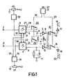
- the modulation signals K 1 and K 2 demodulated by the carrier are fed to input terminals 1 and 2 and fed to the inputs of two adjustable amplifiers 3 and 4.
- the output 5 of the amplifier 3 is connected to a deemphasis element 6 and the input of an impedance converter 7, the output of which is connected to the first input terminal 8 of a modulation type selector switch 10.
- An output 9 of the amplifier 4 is connected to a second de-emphasis element 11 to earth and to the input of a second impedance converter 12, the output of which is connected to the second input terminal 13 of the modulation type selector switch 10.
- the loudspeakers 19 and 20 are connected to the output terminals 15 and 16 of the modulation type selector switch 10 via further signal processing circuits, for example amplifiers 17 and 18, respectively.
- the switch 10 is a four-stage switch, the contacts of which are connected in a known manner so that - counted from above - the signals from the input terminals 8 and 13 arrive separately at the speakers 19 and 20 in the first position shown. In the second position, they are fed together by terminal 8 for the monoaural reproduction of a stereophonic signal. In the third position, the same connection is provided in order to make the information signal K 1 , which corresponds, for example, to the original language of a film, audible via both loudspeakers 19 and 20.
- the signal K 2 is fed from the terminal 13 to both speakers, for example for playback in another language.
- the two changeover switches the tongue of which is located at the output terminals 15 and 16, are actuated by means of an actuation switch 21 which can be brought into one of the four positions by means of a rotary knob 22.
- the effect of this switch 21 is shown by the dashed line 23 to the changeover zones of the changeover switches 15 and 16.
- the actuation switch 21 can also be designed as an electronic control.
- a signal is fed from the output 24 of the amplifier 4 via a switch 25 to the input of the impedance converter 7 in such a way that at point A the difference between the signals from the output 5 of the amplifier 3 and the signal from the output 24 of the amplifier 4 is formed.
- the degree of gain must be adjusted; for this purpose, a connection is established between the outputs 27 and 28 of the amplifier 3 by means of a changeover switch 29 such that the gain is increased by a factor of 2. It would of course also be possible to reduce the amplification of the amplifier 4 to 0.5 in a corresponding manner by means of a changeover switch.
- the changeover switches 25 and 29 are brought into the required position by the actuating switch 21 via an operative connection 30. As you can see, these switches are only closed with stereo reception; for the other types of reception, the gain is not changed and the signals are not dematriated.
- the amplifiers 3 and 4 are designed as cross-coupled differential amplifiers in such a way that the gain can be changed at their control inputs 31 and 32 by means of direct voltages or direct currents.
- These DC control variables are supplied by the outputs 33 and 34 of a differential amplifier 36, the input of which is taken from the tap of a potentiometer 37 connected between the supply source + U and ground.
- the output values of the differential amplifier 36 change in opposite directions, and accordingly the amplification levels of the amplifiers 3 and 4 are changed in opposite directions.
- the amplifiers 3 and 4 also have inputs 37 and 38 which are connected to one another and to the output of a direct current amplifier 39.
- the input of the amplifier 39 is connected to the tap of a potentiometer 40 connected between ground and + U B. By adjusting this tap, the amplification of the amplifiers 3 and 4 can be changed in the same direction. This enables the level to be adjusted for both transmission channels. If necessary, adjustment of the potentiometer 40 can also be used to adjust the volume.
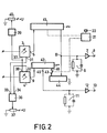
- Strength in F. 2 shows the block diagram according to FIG. 1 with some further details, the same parts being provided with the same reference numerals.
- the switch 10 with the downstream connections to the speakers has been omitted.
- the output 5 of the amplifier 3 controls a current mirror circuit 41
- the output 9 of the amplifier 4 controls a current mirror circuit 42.
- the output of the current mirror circuit 41 is connected to a current node B, which is located at the input of the impedance converter 7.
- a first output 45 of the current mirror circuit 42 is connected to the input of the impedance converter 12.
- a second output 46 of the current mirror circuit 42 is connected via a switch 43 to the input of a third current mirror circuit 44, the output of which is also at the node B and thus at the input of the impedance converter 7.
- the impedance converter 7 with the de-emphasis element 6 connected is thus supplied with a signal which corresponds to the difference between the stereo signals 2 (L + R) and 2R, that is to say 2L.
- the amplifiers 3 and 4 have the same amplification except for slight differences due to the adjustment; likewise, the ratio between the input current and the output current of the current mirrors 41, 42 and 44 is normally the same.
- the signal K is also transmitted from the output terminal 9 via the current mirror circuits 42 and 44 to the node B, the desired dematrification taking place.
- the amplifiers 3 and 4 are therefore not switched over for the factor 2 mentioned, but this adaptation takes place within a current mirror circuit 41 which is provided anyway for signal transmission and decoupling from the output.
- the switch 43 is not in the open state connected to the circuit of the signal K 1 , but it is only between the two current mirror circuits 42 and 44. It can be included in one of the current mirror circuits by blocking a transistor transmitting the signal K 2 by means of a DC switching variable.
Priority Applications (1)
| Application Number | Priority Date | Filing Date | Title |
|---|---|---|---|
| AT82201071T ATE12016T1 (de) | 1981-09-04 | 1982-08-31 | Schaltungsanordnung zum empfangen zweier modulationssignale, insbesondere beim fernsehen. |
Applications Claiming Priority (2)
| Application Number | Priority Date | Filing Date | Title |
|---|---|---|---|
| DE3135060 | 1981-09-04 | ||
| DE19813135060 DE3135060A1 (de) | 1981-09-04 | 1981-09-04 | Schaltungsanordnung zum empfangen zweier modulationssignale, insbesondere beim fernsehen |
Publications (3)
| Publication Number | Publication Date |
|---|---|
| EP0074142A2 true EP0074142A2 (fr) | 1983-03-16 |
| EP0074142A3 EP0074142A3 (en) | 1983-04-27 |
| EP0074142B1 EP0074142B1 (fr) | 1985-02-27 |
Family
ID=6140881
Family Applications (1)
| Application Number | Title | Priority Date | Filing Date |
|---|---|---|---|
| EP82201071A Expired EP0074142B1 (fr) | 1981-09-04 | 1982-08-31 | Arrangement de circuit pour recevoir deux signaux modulés, en particulier pour télévision |
Country Status (8)
| Country | Link |
|---|---|
| US (1) | US4461021A (fr) |
| EP (1) | EP0074142B1 (fr) |
| JP (1) | JPS5848543A (fr) |
| AT (1) | ATE12016T1 (fr) |
| AU (1) | AU549973B2 (fr) |
| DE (2) | DE3135060A1 (fr) |
| ES (1) | ES515423A0 (fr) |
| FI (1) | FI74855C (fr) |
Cited By (1)
| Publication number | Priority date | Publication date | Assignee | Title |
|---|---|---|---|---|
| DE3516024C1 (de) * | 1985-05-04 | 1986-12-04 | Loewe Opta Gmbh, 8640 Kronach | Schaltungsanordnung zum Empfang von nach dem Zweitonträgerverfahren übertragenen stereophonen oder monophonen Fernsehtonsignalen |
Families Citing this family (7)
| Publication number | Priority date | Publication date | Assignee | Title |
|---|---|---|---|---|
| JPS60103748A (ja) * | 1983-11-09 | 1985-06-08 | Sony Corp | デイジタル信号伝送方式 |
| JPS6124380A (ja) * | 1984-07-12 | 1986-02-03 | Nec Corp | テレビ音声多重信号検波用pll回路 |
| US4654707A (en) * | 1985-04-08 | 1987-03-31 | Zenith Electronics Corporation | Method and apparatus for volume control of a BTSC multi-channel sound signal |
| US4688252A (en) * | 1985-12-19 | 1987-08-18 | Zenith Electronics Corporation | IV SAP/stereo audio system |
| KR890016845A (ko) * | 1988-04-30 | 1989-11-30 | 최근선 | Tv수상기의 부음성 지연장치 |
| US5428404A (en) * | 1993-01-29 | 1995-06-27 | Scientific-Atlanta, Inc. | Apparatus for method for selectively demodulating and remodulating alternate channels of a television broadcast |
| DE102005023717A1 (de) * | 2005-05-18 | 2006-11-23 | E.G.O. Elektro-Gerätebau GmbH | Verfahren zur Auswertung eines Potentiometers sowie Schaltungsanordnung mit einem Potentiometer |
Citations (2)
| Publication number | Priority date | Publication date | Assignee | Title |
|---|---|---|---|---|
| DE2827159A1 (de) * | 1978-06-21 | 1980-01-03 | Inst Rundfunktechnik Gmbh | Verfahren zum uebertragen von stereophonen signalen auf zwei gleichwertigen einzelkanaelen, insbesondere zwei-traegerverfahren beim fernsehton |
| EP0056270A1 (fr) * | 1981-01-14 | 1982-07-21 | Matsushita Electric Industrial Co., Ltd. | Appareil démodulateur de signal audio pour un récepteur de télévision |
Family Cites Families (2)
| Publication number | Priority date | Publication date | Assignee | Title |
|---|---|---|---|---|
| DE2902933C3 (de) * | 1979-01-26 | 1983-02-10 | Interessengemeinschaft für Rundfunkschutzrechte GmbH, 4000 Düsseldorf | Einrichtung zum Empfangen von auf zwei gleichwertigen Einzelkanälen übertragenen stereophonen Signalen |
| US4389536A (en) * | 1980-09-24 | 1983-06-21 | Willi Schickedanz | Receiver for a two channel television sound |
-
1981
- 1981-09-04 DE DE19813135060 patent/DE3135060A1/de not_active Withdrawn
-
1982
- 1982-08-31 AT AT82201071T patent/ATE12016T1/de not_active IP Right Cessation
- 1982-08-31 EP EP82201071A patent/EP0074142B1/fr not_active Expired
- 1982-08-31 DE DE8282201071T patent/DE3262479D1/de not_active Expired
- 1982-09-01 FI FI823020A patent/FI74855C/fi not_active IP Right Cessation
- 1982-09-01 AU AU87895/82A patent/AU549973B2/en not_active Ceased
- 1982-09-01 ES ES515423A patent/ES515423A0/es active Granted
- 1982-09-02 JP JP57151837A patent/JPS5848543A/ja active Granted
- 1982-09-02 US US06/414,110 patent/US4461021A/en not_active Expired - Lifetime
Patent Citations (2)
| Publication number | Priority date | Publication date | Assignee | Title |
|---|---|---|---|---|
| DE2827159A1 (de) * | 1978-06-21 | 1980-01-03 | Inst Rundfunktechnik Gmbh | Verfahren zum uebertragen von stereophonen signalen auf zwei gleichwertigen einzelkanaelen, insbesondere zwei-traegerverfahren beim fernsehton |
| EP0056270A1 (fr) * | 1981-01-14 | 1982-07-21 | Matsushita Electric Industrial Co., Ltd. | Appareil démodulateur de signal audio pour un récepteur de télévision |
Cited By (1)
| Publication number | Priority date | Publication date | Assignee | Title |
|---|---|---|---|---|
| DE3516024C1 (de) * | 1985-05-04 | 1986-12-04 | Loewe Opta Gmbh, 8640 Kronach | Schaltungsanordnung zum Empfang von nach dem Zweitonträgerverfahren übertragenen stereophonen oder monophonen Fernsehtonsignalen |
Also Published As
| Publication number | Publication date |
|---|---|
| FI823020L (fi) | 1983-03-05 |
| ES8306300A1 (es) | 1983-05-01 |
| FI74855C (fi) | 1988-03-10 |
| ATE12016T1 (de) | 1985-03-15 |
| ES515423A0 (es) | 1983-05-01 |
| JPS5848543A (ja) | 1983-03-22 |
| FI74855B (fi) | 1987-11-30 |
| EP0074142A3 (en) | 1983-04-27 |
| FI823020A0 (fi) | 1982-09-01 |
| JPH0326575B2 (fr) | 1991-04-11 |
| AU8789582A (en) | 1983-03-10 |
| US4461021A (en) | 1984-07-17 |
| DE3135060A1 (de) | 1983-03-24 |
| EP0074142B1 (fr) | 1985-02-27 |
| AU549973B2 (en) | 1986-02-20 |
| DE3262479D1 (en) | 1985-04-04 |
Similar Documents
| Publication | Publication Date | Title |
|---|---|---|
| DE2351423C2 (de) | Stereophonie-Wiedergabegerät | |
| DE2624568C2 (de) | Stereophones Wiedergabegerät | |
| DE2264023C3 (de) | Dekodierer für ein SQ-Vierkanal-Matrix-System | |
| EP0073929B1 (fr) | Circuit semi-conducteur de traitement de signaux réalisable en circuit intégré | |
| EP0074142B1 (fr) | Arrangement de circuit pour recevoir deux signaux modulés, en particulier pour télévision | |
| DE2511026A1 (de) | Schaltungsanordnung zur kontinuierlichen basisbreiteneinstellung in einem stereodecoder | |
| DE3331352A1 (de) | Schaltungsanordnung und verfahren fuer wahlweisen mono- und stereo-ton-betrieb von ton- und bildrundfunkemfaengern und -recordern | |
| DE3914681A1 (de) | Stereo-expansionsschaltung mit waehlschaltung | |
| DE2649620A1 (de) | Stereo-demodulatorschaltung | |
| DE2062550C3 (de) | UKW-Empfänger für den Empfang monaural oder stereophon ausgestrahlter Sendungen | |
| DE2261519C3 (de) | Vierkanal-Stereophonie-Demodulationssystem | |
| EP0769874A1 (fr) | Assemblage amplificateur audio pour plus de deux canaux de reproduction | |
| DE2902933A1 (de) | Verfahren zum uebertragen von stereophonen signalen auf zwei gleichwertigen einzelkanaelen, insbesondere zwei- traegerverfahren beim fernsehton | |
| DE2645774A1 (de) | Stereosignaldemodulator | |
| DE2218822B2 (de) | Vierkanal-FM-Übertragungs-,ystem | |
| DE3006271C2 (de) | Integrierte Tonsignalschaltung in einem Fernsehempfangsgerät | |
| DE2547289C2 (de) | Anordnung zur Entzerrung differentieller Phasenfehler | |
| DE2026943C3 (de) | Schaltungsanordnung für ein Drahtfunksystem zur Verbindung mehrerer Signalquellen mit einer Vielzahl von Teilnehmern | |
| DE3217230C2 (de) | Anordnung zur wahlweisen Wiedergabe monophoner oder stereophoner Signale | |
| DE2252132C3 (de) | Decodierer für ein 4-2-4-Matrixsystem | |
| DE3217231A1 (de) | Anordnung zur angepassten steuerung der lautstaerke zweier tonkanaele | |
| DE1917895C3 (de) | Vorrichtung zur Bildung pseudostereophoner Ausgangssignale aus einem monophonen Eingangssignal | |
| DE3305940C2 (de) | Schaltung zur Erzeugung eines Raumklangs bei Monobetrieb eines Stereoempfängers | |
| DE2230162A1 (de) | Vorrichtung zur vierton-wiedergabe | |
| DE2910038A1 (de) | Stoerunterdrueckungseinrichtung |
Legal Events
| Date | Code | Title | Description |
|---|---|---|---|
| PUAI | Public reference made under article 153(3) epc to a published international application that has entered the european phase |
Free format text: ORIGINAL CODE: 0009012 |
|
| PUAL | Search report despatched |
Free format text: ORIGINAL CODE: 0009013 |
|
| 17P | Request for examination filed |
Effective date: 19820831 |
|
| AK | Designated contracting states |
Designated state(s): AT BE DE GB IT SE |
|
| AK | Designated contracting states |
Designated state(s): AT BE DE GB IT SE |
|
| ITF | It: translation for a ep patent filed |
Owner name: ING. C. GREGORJ S.P.A. |
|
| GRAA | (expected) grant |
Free format text: ORIGINAL CODE: 0009210 |
|
| AK | Designated contracting states |
Designated state(s): AT BE DE GB IT SE |
|
| REF | Corresponds to: |
Ref document number: 12016 Country of ref document: AT Date of ref document: 19850315 Kind code of ref document: T |
|
| REF | Corresponds to: |
Ref document number: 3262479 Country of ref document: DE Date of ref document: 19850404 |
|
| PLBE | No opposition filed within time limit |
Free format text: ORIGINAL CODE: 0009261 |
|
| STAA | Information on the status of an ep patent application or granted ep patent |
Free format text: STATUS: NO OPPOSITION FILED WITHIN TIME LIMIT |
|
| 26N | No opposition filed | ||
| ITTA | It: last paid annual fee | ||
| EAL | Se: european patent in force in sweden |
Ref document number: 82201071.6 |
|
| ITPR | It: changes in ownership of a european patent |
Owner name: CAMBIO RAGIONE SOCIALE;PHILIPS ELECTRONICS N.V. |
|
| PGFP | Annual fee paid to national office [announced via postgrant information from national office to epo] |
Ref country code: BE Payment date: 19960719 Year of fee payment: 15 |
|
| PGFP | Annual fee paid to national office [announced via postgrant information from national office to epo] |
Ref country code: GB Payment date: 19960731 Year of fee payment: 15 |
|
| PGFP | Annual fee paid to national office [announced via postgrant information from national office to epo] |
Ref country code: SE Payment date: 19960827 Year of fee payment: 15 |
|
| PGFP | Annual fee paid to national office [announced via postgrant information from national office to epo] |
Ref country code: AT Payment date: 19960913 Year of fee payment: 15 |
|
| PGFP | Annual fee paid to national office [announced via postgrant information from national office to epo] |
Ref country code: DE Payment date: 19961025 Year of fee payment: 15 |
|
| PG25 | Lapsed in a contracting state [announced via postgrant information from national office to epo] |
Ref country code: GB Free format text: LAPSE BECAUSE OF NON-PAYMENT OF DUE FEES Effective date: 19970831 Ref country code: BE Free format text: LAPSE BECAUSE OF NON-PAYMENT OF DUE FEES Effective date: 19970831 Ref country code: AT Free format text: LAPSE BECAUSE OF NON-PAYMENT OF DUE FEES Effective date: 19970831 |
|
| PG25 | Lapsed in a contracting state [announced via postgrant information from national office to epo] |
Ref country code: SE Free format text: LAPSE BECAUSE OF NON-PAYMENT OF DUE FEES Effective date: 19970901 |
|
| BERE | Be: lapsed |
Owner name: PHILIPS ELECTRONICS N.V. Effective date: 19970831 |
|
| GBPC | Gb: european patent ceased through non-payment of renewal fee |
Effective date: 19970831 |
|
| PG25 | Lapsed in a contracting state [announced via postgrant information from national office to epo] |
Ref country code: DE Free format text: LAPSE BECAUSE OF NON-PAYMENT OF DUE FEES Effective date: 19980501 |
|
| EUG | Se: european patent has lapsed |
Ref document number: 82201071.6 |