EP0069901A2 - Module à redresseur de courant - Google Patents
Module à redresseur de courant Download PDFInfo
- Publication number
- EP0069901A2 EP0069901A2 EP82105678A EP82105678A EP0069901A2 EP 0069901 A2 EP0069901 A2 EP 0069901A2 EP 82105678 A EP82105678 A EP 82105678A EP 82105678 A EP82105678 A EP 82105678A EP 0069901 A2 EP0069901 A2 EP 0069901A2
- Authority
- EP
- European Patent Office
- Prior art keywords
- housing
- ceramic plate
- interior
- metallizations
- frame
- Prior art date
- Legal status (The legal status is an assumption and is not a legal conclusion. Google has not performed a legal analysis and makes no representation as to the accuracy of the status listed.)
- Granted
Links
Images
Classifications
-
- H—ELECTRICITY
- H01—ELECTRIC ELEMENTS
- H01L—SEMICONDUCTOR DEVICES NOT COVERED BY CLASS H10
- H01L23/00—Details of semiconductor or other solid state devices
- H01L23/02—Containers; Seals
- H01L23/04—Containers; Seals characterised by the shape of the container or parts, e.g. caps, walls
- H01L23/053—Containers; Seals characterised by the shape of the container or parts, e.g. caps, walls the container being a hollow construction and having an insulating or insulated base as a mounting for the semiconductor body
-
- H—ELECTRICITY
- H01—ELECTRIC ELEMENTS
- H01L—SEMICONDUCTOR DEVICES NOT COVERED BY CLASS H10
- H01L23/00—Details of semiconductor or other solid state devices
- H01L23/12—Mountings, e.g. non-detachable insulating substrates
- H01L23/14—Mountings, e.g. non-detachable insulating substrates characterised by the material or its electrical properties
- H01L23/15—Ceramic or glass substrates
-
- H—ELECTRICITY
- H01—ELECTRIC ELEMENTS
- H01L—SEMICONDUCTOR DEVICES NOT COVERED BY CLASS H10
- H01L23/00—Details of semiconductor or other solid state devices
- H01L23/16—Fillings or auxiliary members in containers or encapsulations, e.g. centering rings
- H01L23/18—Fillings characterised by the material, its physical or chemical properties, or its arrangement within the complete device
- H01L23/24—Fillings characterised by the material, its physical or chemical properties, or its arrangement within the complete device solid or gel at the normal operating temperature of the device
-
- H—ELECTRICITY
- H01—ELECTRIC ELEMENTS
- H01L—SEMICONDUCTOR DEVICES NOT COVERED BY CLASS H10
- H01L23/00—Details of semiconductor or other solid state devices
- H01L23/48—Arrangements for conducting electric current to or from the solid state body in operation, e.g. leads, terminal arrangements ; Selection of materials therefor
- H01L23/488—Arrangements for conducting electric current to or from the solid state body in operation, e.g. leads, terminal arrangements ; Selection of materials therefor consisting of soldered or bonded constructions
- H01L23/495—Lead-frames or other flat leads
- H01L23/49541—Geometry of the lead-frame
- H01L23/49562—Geometry of the lead-frame for devices being provided for in H01L29/00
-
- H—ELECTRICITY
- H01—ELECTRIC ELEMENTS
- H01L—SEMICONDUCTOR DEVICES NOT COVERED BY CLASS H10
- H01L2924/00—Indexing scheme for arrangements or methods for connecting or disconnecting semiconductor or solid-state bodies as covered by H01L24/00
- H01L2924/0001—Technical content checked by a classifier
- H01L2924/0002—Not covered by any one of groups H01L24/00, H01L24/00 and H01L2224/00
-
- Y—GENERAL TAGGING OF NEW TECHNOLOGICAL DEVELOPMENTS; GENERAL TAGGING OF CROSS-SECTIONAL TECHNOLOGIES SPANNING OVER SEVERAL SECTIONS OF THE IPC; TECHNICAL SUBJECTS COVERED BY FORMER USPC CROSS-REFERENCE ART COLLECTIONS [XRACs] AND DIGESTS
- Y10—TECHNICAL SUBJECTS COVERED BY FORMER USPC
- Y10S—TECHNICAL SUBJECTS COVERED BY FORMER USPC CROSS-REFERENCE ART COLLECTIONS [XRACs] AND DIGESTS
- Y10S257/00—Active solid-state devices, e.g. transistors, solid-state diodes
- Y10S257/909—Macrocell arrays, e.g. gate arrays with variable size or configuration of cells
Definitions
- the invention relates to a converter module with a frame that is open at the top and bottom as the housing wall and a ceramic plate that is glued to the frame as the housing base, the ceramic plate on its side facing the housing interior having metallizations that serve as conductor tracks for soldering to semiconductor components, internal connecting lugs and external ones Connection elements are used, the connection elements being designed as freely accessible flat plugs on the upper side of the housing and soldered in the housing with a metallization, and the housing being poured out about half with a sealing compound.
- Such a converter module is known from the brochure BBC rectifier bridges of high power, DHS 104981 / 29D.
- thyristors and diodes are used as semiconductor components.
- Fully controlled and semi-controlled single-phase bridges can be implemented by means of such converter modules.
- the heating causes a local thermal load on the ceramic plate via the heating metallizations on the side of the ceramic plate facing the interior of the housing. This heat loss must be dissipated to the heat sink using the lowest possible heat resistance. Attaching a potential-free metal base plate does not bring the hoped-for success, since this metal base plate becomes slightly hollow towards the center of the plate due to the "bimetal effect" when the ceramic substrate / metal plate system is soldered together with an intermediate solder layer. Despite sufficient application of thermal paste, there is a risk of including thin layers of air, which increase the thermal resistance between the metal base plate and the heat sink.
- the metal base plate is omitted in a known solution, so that the ceramic is in direct contact with the heat sink.
- This version has fewer heat transfers, but it has the disadvantage that the ceramic plate when handling the Module can easily be damaged. This would result in a loss of insulation.
- the object of the invention is to create a converter module of the type mentioned at the outset, in which the thermal voltages which occur during operation cannot lead to a defect in the module.
- the ceramic plate is provided on its side facing away from the inside of the housing with a copper foil, the thickness of the copper foil being approximately equal to the thickness of the metallizations and in that the tabs have an expansion curve between a widened solderable foot part and the actual plug connection , wherein the cross section of the expansion elbow is smaller than the cross section of the rest of the flat connector.
- the converter module can be produced inexpensively and ensures good heat transfer to the heat sink.
- thermal stresses caused by "bimetal effects" are avoided.
- the brittle and break-sensitive ceramic substrate is additionally protected, i.e. If the heat sink is uneven and there are dust grains on the mounting surfaces, there is no risk of ceramic breakage and thus the loss of the insulation capacity between the internal electrical connections of the converter module and the heat sink.
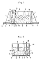
- the module has a frame 1 open at the top and bottom, which serves as the housing wall.
- the frame 1 has stiffening edges 2 on its two narrow sides.
- the frame 1 also has a plurality of ribs 3 running parallel to the broad side or narrow side.
- two ribs 3 run parallel to the broad side and two ribs 3 parallel to the narrow side. This results in nine rectangular cells for receiving external connection elements for the module.
- the ribs 3 serve at the same time as insulation and creepage extension between the external connection elements.
- the frame 1 has fastening tabs 4 on its two narrow sides at the level of the bottom surface. These fastening tabs 4 are provided with bores or U-shaped recesses 5 for mounting the converter module on a heat sink.
- the housing of the converter module is formed on the one hand by the frame 1 and on the other hand by a ceramic plate 6 placed in a recess in the bottom surface of the open frame 1.
- the ceramic plate 6 has metallizations 7 on its surface facing the interior of the housing. These metallizations 7 are realized, for example, by copper foil, which, according to the method known from patent application P 30 36 128.5, directly without an intermediate layer are applied to the ceramic.
- the metallizations 7 serve as conductor tracks and contact areas for soldering on connection elements, semiconductor components and internal connecting tabs.
- a thick copper foil 8 is likewise applied directly to the side of the ceramic plate 6 facing away from the interior of the housing, in accordance with the method according to patent application P 30 26 128.5.
- the thickness of the copper foil 8 corresponds approximately to the thickness of the metallizations 7 (preferably also copper foils). This effectively prevents tension resulting from the manufacturing processes and the one-sided soldering processes on the side of the ceramic plate 6 facing the interior of the housing.
- the copper foil 8 enables good thermal contact with a heat sink connected to the module. The risk of ceramic breakage due to uneven and dirty (dust grains) heat sinks is also significantly lower.
- the frame 1 and the ceramic plate 6 are glued together.
- the frame 1 has the aforementioned circumferential depression in its bottom surface, the depth of which approximately corresponds to the thickness of the ceramic plate 6.
- a circumferential groove 9 provided in this recess of the frame 1 serves to receive emerging adhesive. The excess adhesive migrates into the groove 9 and does not swell over the edge of the ceramic plate 6 onto the cooling surface.
- a cooling surface of the ceramic plate 6 which is contaminated with the adhesive swelling out would have to be additionally processed in a disadvantageous manner in order to remove the adhesive residues. Otherwise the heat transfer to the heat sink would be impeded.
- a flat plug 10 is soldered to the metallization 7 as a connection element for an external plug contact.
- the tab 10 is freely accessible on the top of the housing. It has a widened foot part 11 for mechanical stabilization of the solder joint on the metallization 7.
- the widened foot part 11 is followed by an angled portion 12 and an expansion bend 13.
- the embodiment of the bend 12 and the expansion curve 13 can be seen in particular from FIG. 2.
- the expansion bend 13 merges at its upper end into the actual plug connection 14 with notches 17.
- the cross section of the expansion elbow 13 is smaller than the cross sections of the upper plug connection 14 and the lower foot part 11.
- the expansion elbow 13 avoids high cyclical tensile stresses on the soldered connection between the foot part 11 and the metallization 7 of the ceramic plate 6.
- the lower part of the housing which is glued to the ceramic plate 6 and equipped with semiconductor components and flat plugs, is cast with a soft casting compound (e.g. silicone rubber) to protect the sensitive active parts, and the expansion bend 13 of the flat plug 10 should be fully cast with silicone rubber 15.
- a soft casting compound e.g. silicone rubber
- the housing is sealed to just above the center of the housing using a hard potting compound 16 (e.g. epoxy resin). Due to the hard casting compound 16, the tabs 10 in particular are mechanically stabilized at their notches 17.
- Fig. 2 is a section through the narrow side of the stream judge module shown.
- the frame 1 with the ribs 3 and the circumferential groove 9 for receiving adhesive residue can be seen.
- the ceramic plate 6 forming the housing base is coated on the one hand with the metallization 7 and on the other hand with the copper foil 8.
- the tab 10 is soldered to the metallization 7 with its foot part 11.
- the foot part 11 passes over the bend into the expansion curve 13, to which the actual plug connection 14 connects.
- the soft casting compound 15 cast in the lower housing part and the hard casting compound 16 cast in the middle housing part are shown.
- the upper part of the housing remains free of potting compounds for external connection of the flat plug.
Priority Applications (1)
| Application Number | Priority Date | Filing Date | Title |
|---|---|---|---|
| AT82105678T ATE26505T1 (de) | 1981-07-11 | 1982-06-26 | Stromrichtermodul. |
Applications Claiming Priority (2)
| Application Number | Priority Date | Filing Date | Title |
|---|---|---|---|
| DE3127457 | 1981-07-11 | ||
| DE3127457A DE3127457C2 (de) | 1981-07-11 | 1981-07-11 | Stromrichtermodul |
Publications (3)
| Publication Number | Publication Date |
|---|---|
| EP0069901A2 true EP0069901A2 (fr) | 1983-01-19 |
| EP0069901A3 EP0069901A3 (en) | 1984-11-21 |
| EP0069901B1 EP0069901B1 (fr) | 1987-04-08 |
Family
ID=6136700
Family Applications (1)
| Application Number | Title | Priority Date | Filing Date |
|---|---|---|---|
| EP82105678A Expired EP0069901B1 (fr) | 1981-07-11 | 1982-06-26 | Module à redresseur de courant |
Country Status (4)
| Country | Link |
|---|---|
| US (1) | US4670771A (fr) |
| EP (1) | EP0069901B1 (fr) |
| AT (1) | ATE26505T1 (fr) |
| DE (1) | DE3127457C2 (fr) |
Cited By (10)
| Publication number | Priority date | Publication date | Assignee | Title |
|---|---|---|---|---|
| EP0118022A2 (fr) * | 1983-03-04 | 1984-09-12 | BROWN, BOVERI & CIE Aktiengesellschaft | Module à redresseur ayant une pièce de fixation |
| EP0144866A2 (fr) * | 1983-11-25 | 1985-06-19 | Kabushiki Kaisha Toshiba | Dispositif semi-conducteur comprenant un substrat |
| EP0155473A1 (fr) * | 1984-02-23 | 1985-09-25 | BROWN, BOVERI & CIE Aktiengesellschaft | Module pour dispositifs semiconducteurs de puissance et son procédé de fabrication |
| DE3521572A1 (de) * | 1985-06-15 | 1986-12-18 | Brown, Boveri & Cie Ag, 6800 Mannheim | Leistungshalbleitermodul mit keramiksubstrat |
| EP0237739A2 (fr) * | 1986-02-15 | 1987-09-23 | Asea Brown Boveri Aktiengesellschaft | Module à semi-conducteur de puissance et procédé pour fabriquer le module |
| EP0243637A2 (fr) * | 1986-03-26 | 1987-11-04 | Asea Brown Boveri Aktiengesellschaft | Module de puissance à semi-conducteur |
| EP0398108A1 (fr) * | 1989-05-13 | 1990-11-22 | Asea Brown Boveri Aktiengesellschaft | Boîtier en plastique et module semi-conducteur de puissance comprenant ce boîtier |
| FR2668302A1 (fr) * | 1990-10-17 | 1992-04-24 | Nec Corp | Boitier comportant un ou plusieurs circuits integres et procede de fabrication de ce boitier. |
| EP0650191A1 (fr) * | 1991-02-20 | 1995-04-26 | Nec Corporation | Structure de chip à circuit intégré |
| DE19615481C5 (de) * | 1996-04-03 | 2013-03-14 | Curamik Electronics Gmbh | Gewölbtes Metall-Keramik-Substrat |
Families Citing this family (22)
| Publication number | Priority date | Publication date | Assignee | Title |
|---|---|---|---|---|
| DE3604075A1 (de) * | 1986-02-08 | 1987-08-13 | Bosch Gmbh Robert | Verpackung von leistungsbauelementen |
| DE3604313A1 (de) * | 1986-02-12 | 1987-08-13 | Bbc Brown Boveri & Cie | Leistungshalbleitermodul |
| DE3621994A1 (de) * | 1986-07-01 | 1988-01-14 | Bbc Brown Boveri & Cie | Leistungshalbleitermodul |
| DE8703604U1 (fr) * | 1987-03-11 | 1988-07-21 | Euroatlas Gmbh Fuer Umformertechnik Und Optronik, 2800 Bremen, De | |
| DE3717489A1 (de) * | 1987-05-23 | 1988-12-01 | Asea Brown Boveri | Leistungshalbleitermodul und verfahren zur herstellung des moduls |
| US4739449A (en) * | 1987-06-30 | 1988-04-19 | Kaufman Lance R | Circuit package with thermal expansion relief chimney |
| DE3728096C1 (en) * | 1987-07-03 | 1989-01-12 | Duerrwaechter E Dr Doduco | Flat body, especially for use as a heat sink for electronic power components |
| US5027255A (en) * | 1988-10-22 | 1991-06-25 | Westinghouse Electric Co. | High performance, high current miniaturized low voltage power supply |
| DE3837920A1 (de) * | 1988-11-09 | 1990-05-10 | Semikron Elektronik Gmbh | Halbleiterelement |
| DE3900512A1 (de) * | 1989-01-10 | 1990-07-19 | Tucker Gmbh Bostik | Halbleiterbauelement fuer ein schaltnetzteil |
| DE4001554A1 (de) * | 1990-01-20 | 1991-07-25 | Abb Ixys Semiconductor Gmbh | Leistungshalbleitermodul |
| US5243217A (en) * | 1990-11-03 | 1993-09-07 | Fuji Electric Co., Ltd. | Sealed semiconductor device with protruding portion |
| JP2850606B2 (ja) * | 1991-11-25 | 1999-01-27 | 富士電機株式会社 | トランジスタモジュール |
| AT406434B (de) * | 1993-12-23 | 2000-05-25 | Ixys Semiconductor Gmbh | Vorrichtung zur umformung eines dreiphasigen spannungssystems in eine vorgebbare, einen verbraucher speisende gleichspannung |
| DE4446527A1 (de) * | 1994-12-24 | 1996-06-27 | Ixys Semiconductor Gmbh | Leistungshalbleitermodul |
| JP3206717B2 (ja) * | 1996-04-02 | 2001-09-10 | 富士電機株式会社 | 電力用半導体モジュール |
| DE19725843C1 (de) * | 1997-06-18 | 1998-10-29 | Siemens Matsushita Components | Elektrischer Kondensator |
| DE19818036B4 (de) * | 1998-04-22 | 2005-05-19 | Siemens Ag | Verfahren zur Herstellung eines elektrotechnischen Bauteils mit einer kunststoffpassivierten Oberfläche, derartiges Bauteil und Anwendung dieses Bauteils |
| EP2334370B1 (fr) * | 2008-09-10 | 2018-12-12 | Heartware, Inc. | Système tet pour dispositif médical implanté |
| US8847328B1 (en) | 2013-03-08 | 2014-09-30 | Ixys Corporation | Module and assembly with dual DC-links for three-level NPC applications |
| US9620877B2 (en) | 2014-06-17 | 2017-04-11 | Semiconductor Components Industries, Llc | Flexible press fit pins for semiconductor packages and related methods |
| US9431311B1 (en) | 2015-02-19 | 2016-08-30 | Semiconductor Components Industries, Llc | Semiconductor package with elastic coupler and related methods |
Citations (2)
| Publication number | Priority date | Publication date | Assignee | Title |
|---|---|---|---|---|
| DE2840514A1 (de) * | 1977-09-19 | 1979-03-22 | Gentron Corp | Leistungssteuergeraet und verfahren zum anbringen desselben |
| DE2819327A1 (de) * | 1978-05-03 | 1979-12-13 | Semikron Gleichrichterbau | Halbleiterbaueinheit |
Family Cites Families (12)
| Publication number | Priority date | Publication date | Assignee | Title |
|---|---|---|---|---|
| US3265805A (en) * | 1964-02-03 | 1966-08-09 | Power Components Inc | Semiconductor power device |
| US3370207A (en) * | 1964-02-24 | 1968-02-20 | Gen Electric | Multilayer contact system for semiconductor devices including gold and copper layers |
| DE1564749A1 (de) * | 1966-10-27 | 1970-01-08 | Semikron Gleichrichterbau | Halbleiteranordnung |
| US3475662A (en) * | 1967-11-22 | 1969-10-28 | Westinghouse Electric Corp | Hermetically sealed electrical device |
| US3829598A (en) * | 1972-09-25 | 1974-08-13 | Hutson Ind Inc | Copper heat sinks for electronic devices and method of making same |
| US3994430A (en) * | 1975-07-30 | 1976-11-30 | General Electric Company | Direct bonding of metals to ceramics and metals |
| JPS5315763A (en) * | 1976-07-28 | 1978-02-14 | Hitachi Ltd | Resin sealed type semiconductor device |
| US4117508A (en) * | 1977-03-21 | 1978-09-26 | General Electric Company | Pressurizable semiconductor pellet assembly |
| US4249034A (en) * | 1978-11-27 | 1981-02-03 | General Electric Company | Semiconductor package having strengthening and sealing upper chamber |
| DE3028178C2 (de) * | 1980-07-25 | 1985-05-09 | Brown, Boveri & Cie Ag, 6800 Mannheim | Leistungshalbleiter-Modul |
| DE3036128C2 (de) * | 1980-09-25 | 1983-08-18 | Brown, Boveri & Cie Ag, 6800 Mannheim | Verfahren zum direkten Verbinden von Kupferfolien mit Oxidkeramiksubstraten |
| US4514587A (en) * | 1981-12-23 | 1985-04-30 | Unitrode Corporation | High power semiconductor package |
-
1981
- 1981-07-11 DE DE3127457A patent/DE3127457C2/de not_active Expired
-
1982
- 1982-06-26 EP EP82105678A patent/EP0069901B1/fr not_active Expired
- 1982-06-26 AT AT82105678T patent/ATE26505T1/de not_active IP Right Cessation
-
1985
- 1985-08-02 US US06/762,802 patent/US4670771A/en not_active Expired - Lifetime
Patent Citations (2)
| Publication number | Priority date | Publication date | Assignee | Title |
|---|---|---|---|---|
| DE2840514A1 (de) * | 1977-09-19 | 1979-03-22 | Gentron Corp | Leistungssteuergeraet und verfahren zum anbringen desselben |
| DE2819327A1 (de) * | 1978-05-03 | 1979-12-13 | Semikron Gleichrichterbau | Halbleiterbaueinheit |
Cited By (16)
| Publication number | Priority date | Publication date | Assignee | Title |
|---|---|---|---|---|
| EP0118022A3 (en) * | 1983-03-04 | 1985-11-06 | Brown, Boveri & Cie Aktiengesellschaft | Rectifier module with fastening part |
| EP0118022A2 (fr) * | 1983-03-04 | 1984-09-12 | BROWN, BOVERI & CIE Aktiengesellschaft | Module à redresseur ayant une pièce de fixation |
| EP0144866A2 (fr) * | 1983-11-25 | 1985-06-19 | Kabushiki Kaisha Toshiba | Dispositif semi-conducteur comprenant un substrat |
| EP0144866B1 (fr) * | 1983-11-25 | 1988-09-07 | Kabushiki Kaisha Toshiba | Dispositif semi-conducteur comprenant un substrat |
| EP0155473A1 (fr) * | 1984-02-23 | 1985-09-25 | BROWN, BOVERI & CIE Aktiengesellschaft | Module pour dispositifs semiconducteurs de puissance et son procédé de fabrication |
| DE3521572A1 (de) * | 1985-06-15 | 1986-12-18 | Brown, Boveri & Cie Ag, 6800 Mannheim | Leistungshalbleitermodul mit keramiksubstrat |
| EP0205746A2 (fr) * | 1985-06-15 | 1986-12-30 | Asea Brown Boveri Aktiengesellschaft | Module semi-conducteur de puissance comprenant un substrat céramique |
| EP0205746A3 (en) * | 1985-06-15 | 1987-07-22 | Brown, Boveri & Cie Aktiengesellschaft | Semiconductor power module comprising a ceramic substrate |
| EP0237739A3 (fr) * | 1986-02-15 | 1989-03-15 | Asea Brown Boveri Aktiengesellschaft | Module à semi-conducteur de puissance et procédé pour fabriquer le module |
| EP0237739A2 (fr) * | 1986-02-15 | 1987-09-23 | Asea Brown Boveri Aktiengesellschaft | Module à semi-conducteur de puissance et procédé pour fabriquer le module |
| EP0243637A2 (fr) * | 1986-03-26 | 1987-11-04 | Asea Brown Boveri Aktiengesellschaft | Module de puissance à semi-conducteur |
| EP0243637A3 (en) * | 1986-03-26 | 1990-05-16 | Asea Brown Boveri Aktiengesellschaft | Semi-conductor power module |
| EP0398108A1 (fr) * | 1989-05-13 | 1990-11-22 | Asea Brown Boveri Aktiengesellschaft | Boîtier en plastique et module semi-conducteur de puissance comprenant ce boîtier |
| FR2668302A1 (fr) * | 1990-10-17 | 1992-04-24 | Nec Corp | Boitier comportant un ou plusieurs circuits integres et procede de fabrication de ce boitier. |
| EP0650191A1 (fr) * | 1991-02-20 | 1995-04-26 | Nec Corporation | Structure de chip à circuit intégré |
| DE19615481C5 (de) * | 1996-04-03 | 2013-03-14 | Curamik Electronics Gmbh | Gewölbtes Metall-Keramik-Substrat |
Also Published As
| Publication number | Publication date |
|---|---|
| DE3127457A1 (de) | 1983-02-03 |
| ATE26505T1 (de) | 1987-04-15 |
| EP0069901A3 (en) | 1984-11-21 |
| US4670771A (en) | 1987-06-02 |
| DE3127457C2 (de) | 1985-09-12 |
| EP0069901B1 (fr) | 1987-04-08 |
Similar Documents
| Publication | Publication Date | Title |
|---|---|---|
| EP0069901B1 (fr) | Module à redresseur de courant | |
| DE10149580B4 (de) | Halbleitervorrichtung | |
| DE19601372B4 (de) | Halbleitermodul | |
| DE10031678C2 (de) | Leistungsmodul | |
| DE19921109B4 (de) | Elektronikbauteil und Elektronikkomponente mit einem Keramikbauteilelement | |
| DE19941872B4 (de) | Elektronikkomponente, wie z.B. ein Akustikoberflächenwellenbauelement, und Verfahren zum Herstellen derselben | |
| DE102006037118B3 (de) | Halbleiterschaltmodul für Bordnetze mit mehreren Halbleiterchips, Verwendung eines solchen Halbleiterschaltmoduls und Verfahren zur Herstellung desselben | |
| EP0111659B1 (fr) | Module de transistor de puissance | |
| DE3241508C2 (fr) | ||
| DE19625240A1 (de) | Halbleitervorrichtung | |
| DE3221199A1 (de) | Halbleiteranordnung des isolierten typs | |
| DE19518753A1 (de) | Halbleitervorrichtung und Verfahren zu ihrer Herstellung | |
| DE102005049687A1 (de) | Leistungshalbleiterbauteil in Flachleitertechnik mit vertikalem Strompfad | |
| EP0292848B1 (fr) | Module de puissance à semi-conducteur et son procédé de fabrication | |
| DE102016203581A1 (de) | Halbleitervorrichtung und verfahren zum herstellen einer halbleitervorrichtung | |
| DE69923374T2 (de) | Halbleitervorrichtung | |
| DE212018000073U1 (de) | Halbleiterbauelement | |
| DE102014104856A1 (de) | Explosionsgeschütztes Leistungshalbleitermodul | |
| CH663491A5 (en) | Electronic circuit module | |
| DE10221857A1 (de) | Verfahren zum Befestigen eines Halbleiterchips in einem Kunststoffgehäusekörper, optoelektronisches Halbleiterbauelement und Verfahren zu dessen Herstellung | |
| DE3243689C2 (fr) | ||
| DE2937051A1 (de) | Flachpaket zur aufnahme von elektrischen mikroschaltkreisen und verfahren zu seiner herstellung | |
| EP1595287B1 (fr) | Composant electronique dote d'une puce a semi-conducteurs et procede de fabrication associe | |
| EP1324386A1 (fr) | Module semi-conductrice et methode de fabrication d'une module semi-conductrice | |
| DE3432449C2 (fr) |
Legal Events
| Date | Code | Title | Description |
|---|---|---|---|
| PUAI | Public reference made under article 153(3) epc to a published international application that has entered the european phase |
Free format text: ORIGINAL CODE: 0009012 |
|
| AK | Designated contracting states |
Designated state(s): AT FR GB IT NL SE |
|
| PUAL | Search report despatched |
Free format text: ORIGINAL CODE: 0009013 |
|
| AK | Designated contracting states |
Designated state(s): AT FR GB IT NL SE |
|
| 17P | Request for examination filed |
Effective date: 19841201 |
|
| 17Q | First examination report despatched |
Effective date: 19860225 |
|
| GRAA | (expected) grant |
Free format text: ORIGINAL CODE: 0009210 |
|
| AK | Designated contracting states |
Kind code of ref document: B1 Designated state(s): AT FR GB IT NL SE |
|
| REF | Corresponds to: |
Ref document number: 26505 Country of ref document: AT Date of ref document: 19870415 Kind code of ref document: T |
|
| ET | Fr: translation filed | ||
| ITF | It: translation for a ep patent filed |
Owner name: DE DOMINICIS & MAYER S.R.L. |
|
| PLBE | No opposition filed within time limit |
Free format text: ORIGINAL CODE: 0009261 |
|
| STAA | Information on the status of an ep patent application or granted ep patent |
Free format text: STATUS: NO OPPOSITION FILED WITHIN TIME LIMIT |
|
| 26N | No opposition filed | ||
| PGFP | Annual fee paid to national office [announced via postgrant information from national office to epo] |
Ref country code: AT Payment date: 19900425 Year of fee payment: 9 |
|
| PGFP | Annual fee paid to national office [announced via postgrant information from national office to epo] |
Ref country code: SE Payment date: 19900525 Year of fee payment: 9 |
|
| PGFP | Annual fee paid to national office [announced via postgrant information from national office to epo] |
Ref country code: NL Payment date: 19900630 Year of fee payment: 9 |
|
| PG25 | Lapsed in a contracting state [announced via postgrant information from national office to epo] |
Ref country code: AT Effective date: 19910626 |
|
| PG25 | Lapsed in a contracting state [announced via postgrant information from national office to epo] |
Ref country code: SE Effective date: 19910627 |
|
| ITTA | It: last paid annual fee | ||
| PG25 | Lapsed in a contracting state [announced via postgrant information from national office to epo] |
Ref country code: NL Effective date: 19920101 |
|
| NLV4 | Nl: lapsed or anulled due to non-payment of the annual fee | ||
| EUG | Se: european patent has lapsed |
Ref document number: 82105678.5 Effective date: 19920109 |
|
| REG | Reference to a national code |
Ref country code: FR Ref legal event code: TP Ref country code: FR Ref legal event code: CD |
|
| REG | Reference to a national code |
Ref country code: GB Ref legal event code: 732E |
|
| PGFP | Annual fee paid to national office [announced via postgrant information from national office to epo] |
Ref country code: GB Payment date: 20010522 Year of fee payment: 20 |
|
| PGFP | Annual fee paid to national office [announced via postgrant information from national office to epo] |
Ref country code: FR Payment date: 20010621 Year of fee payment: 20 |
|
| REG | Reference to a national code |
Ref country code: GB Ref legal event code: IF02 |
|
| PG25 | Lapsed in a contracting state [announced via postgrant information from national office to epo] |
Ref country code: GB Free format text: LAPSE BECAUSE OF EXPIRATION OF PROTECTION Effective date: 20020625 |
|
| REG | Reference to a national code |
Ref country code: GB Ref legal event code: PE20 Effective date: 20020625 |