EP0069901A2 - Current rectifier module - Google Patents
Current rectifier module Download PDFInfo
- Publication number
- EP0069901A2 EP0069901A2 EP82105678A EP82105678A EP0069901A2 EP 0069901 A2 EP0069901 A2 EP 0069901A2 EP 82105678 A EP82105678 A EP 82105678A EP 82105678 A EP82105678 A EP 82105678A EP 0069901 A2 EP0069901 A2 EP 0069901A2
- Authority
- EP
- European Patent Office
- Prior art keywords
- housing
- ceramic plate
- interior
- metallizations
- frame
- Prior art date
- Legal status (The legal status is an assumption and is not a legal conclusion. Google has not performed a legal analysis and makes no representation as to the accuracy of the status listed.)
- Granted
Links
Images
Classifications
-
- H—ELECTRICITY
- H01—ELECTRIC ELEMENTS
- H01L—SEMICONDUCTOR DEVICES NOT COVERED BY CLASS H10
- H01L23/00—Details of semiconductor or other solid state devices
- H01L23/02—Containers; Seals
- H01L23/04—Containers; Seals characterised by the shape of the container or parts, e.g. caps, walls
- H01L23/053—Containers; Seals characterised by the shape of the container or parts, e.g. caps, walls the container being a hollow construction and having an insulating or insulated base as a mounting for the semiconductor body
-
- H—ELECTRICITY
- H01—ELECTRIC ELEMENTS
- H01L—SEMICONDUCTOR DEVICES NOT COVERED BY CLASS H10
- H01L23/00—Details of semiconductor or other solid state devices
- H01L23/12—Mountings, e.g. non-detachable insulating substrates
- H01L23/14—Mountings, e.g. non-detachable insulating substrates characterised by the material or its electrical properties
- H01L23/15—Ceramic or glass substrates
-
- H—ELECTRICITY
- H01—ELECTRIC ELEMENTS
- H01L—SEMICONDUCTOR DEVICES NOT COVERED BY CLASS H10
- H01L23/00—Details of semiconductor or other solid state devices
- H01L23/16—Fillings or auxiliary members in containers or encapsulations, e.g. centering rings
- H01L23/18—Fillings characterised by the material, its physical or chemical properties, or its arrangement within the complete device
- H01L23/24—Fillings characterised by the material, its physical or chemical properties, or its arrangement within the complete device solid or gel at the normal operating temperature of the device
-
- H—ELECTRICITY
- H01—ELECTRIC ELEMENTS
- H01L—SEMICONDUCTOR DEVICES NOT COVERED BY CLASS H10
- H01L23/00—Details of semiconductor or other solid state devices
- H01L23/48—Arrangements for conducting electric current to or from the solid state body in operation, e.g. leads, terminal arrangements ; Selection of materials therefor
- H01L23/488—Arrangements for conducting electric current to or from the solid state body in operation, e.g. leads, terminal arrangements ; Selection of materials therefor consisting of soldered or bonded constructions
- H01L23/495—Lead-frames or other flat leads
- H01L23/49541—Geometry of the lead-frame
- H01L23/49562—Geometry of the lead-frame for devices being provided for in H01L29/00
-
- H—ELECTRICITY
- H01—ELECTRIC ELEMENTS
- H01L—SEMICONDUCTOR DEVICES NOT COVERED BY CLASS H10
- H01L2924/00—Indexing scheme for arrangements or methods for connecting or disconnecting semiconductor or solid-state bodies as covered by H01L24/00
- H01L2924/0001—Technical content checked by a classifier
- H01L2924/0002—Not covered by any one of groups H01L24/00, H01L24/00 and H01L2224/00
-
- Y—GENERAL TAGGING OF NEW TECHNOLOGICAL DEVELOPMENTS; GENERAL TAGGING OF CROSS-SECTIONAL TECHNOLOGIES SPANNING OVER SEVERAL SECTIONS OF THE IPC; TECHNICAL SUBJECTS COVERED BY FORMER USPC CROSS-REFERENCE ART COLLECTIONS [XRACs] AND DIGESTS
- Y10—TECHNICAL SUBJECTS COVERED BY FORMER USPC
- Y10S—TECHNICAL SUBJECTS COVERED BY FORMER USPC CROSS-REFERENCE ART COLLECTIONS [XRACs] AND DIGESTS
- Y10S257/00—Active solid-state devices, e.g. transistors, solid-state diodes
- Y10S257/909—Macrocell arrays, e.g. gate arrays with variable size or configuration of cells
Landscapes
- Engineering & Computer Science (AREA)
- Power Engineering (AREA)
- General Physics & Mathematics (AREA)
- Condensed Matter Physics & Semiconductors (AREA)
- Computer Hardware Design (AREA)
- Microelectronics & Electronic Packaging (AREA)
- Physics & Mathematics (AREA)
- Chemical & Material Sciences (AREA)
- Dispersion Chemistry (AREA)
- Ceramic Engineering (AREA)
- Cooling Or The Like Of Semiconductors Or Solid State Devices (AREA)
- Emergency Protection Circuit Devices (AREA)
- Input Circuits Of Receivers And Coupling Of Receivers And Audio Equipment (AREA)
- Rectifiers (AREA)
Abstract
Description
Die Erfindung bezieht sich auf ein Stromrichtermodul mit einem oben und unten offenen Rahmen als Gehäusewandung und einer mit dem Rahmen verklebten Keramikplatte als Gehäuseboden, wobei die Keramikplatte auf ihrer dem Gehäuseinneren zugewandten Seite Metallisierungen aufweist, die als Leiterbahnen zum Verlöten mit Halbleiterbauelementen, internen Verbindungslaschen und externen Anschlußelementen dienen, wobei die Anschlußelemente als auf der Oberseite des Gehäuses frei zugängliche und im Gehäuse mit einer Metallisierung verlötete Flachstecker ausgebildet sind und wobei das Gehäuse mit einer Vergußmasse etwa zur Hälfte ausgegossen ist.The invention relates to a converter module with a frame that is open at the top and bottom as the housing wall and a ceramic plate that is glued to the frame as the housing base, the ceramic plate on its side facing the housing interior having metallizations that serve as conductor tracks for soldering to semiconductor components, internal connecting lugs and external ones Connection elements are used, the connection elements being designed as freely accessible flat plugs on the upper side of the housing and soldered in the housing with a metallization, and the housing being poured out about half with a sealing compound.
Ein derartiges Stromrichtermodul ist bekannt aus dem Prospekt BBC-Gleichrichter-Brücken hoher Leistung, DHS 104981/29D. Als Halbleiterbauelemente werden dabei insbesondere Thyristoren und Dioden eingesetzt. Mittels derartiger Stromrichtermodule sind vollgesteuerte und halbgesteuerte Einphasenbrücken realisierbar.Such a converter module is known from the brochure BBC rectifier bridges of high power, DHS 104981 / 29D. In particular, thyristors and diodes are used as semiconductor components. Fully controlled and semi-controlled single-phase bridges can be implemented by means of such converter modules.
Bei normaler Betriebsbelastung des Stromrichtermoduls entsteht im Gehäuseinneren des Moduls Verlustwärme. Dabei dehnt sich die weiche Silikon-Vergußmasse im Gehäuseinneren wegen ihres etwa um eine Größenordnung höheren Ausdehnungskoeffizienten stärker aus als die metallenen, mit der Keramikplatte verbundenen Flachstecker, so daß an diesen starke zyklische Zugspannungen auftreten. Die Flachstecker sind auf dem Substrat mit Weichlot angelötet. Weichlote reagieren jedoch empfindlich auf zyklische Belastungen, es besteht also die Gefahr, daß nach einer Vielzahl von Lastwechselspielen die innere elektrische Verbindung zwischen Anschlußelement und Substrat unterbrochen wird.With normal operating load of the converter module, heat loss is generated inside the module. The soft silicone potting compound expands more inside the housing because of its expansion coefficient, which is about an order of magnitude higher than the metal tabs connected to the ceramic plate, so that strong cyclic tensile stresses occur on them. The tabs are soldered to the substrate with soft solder. However, soft solders are sensitive to cyclic loads, so there is a risk that the internal electrical connection between the connection element and the substrate will be interrupted after a large number of load cycles.
Ferner bewirkt die Erwärmung beim Betrieb des Stromrichtermoduls eine lokale thermische Belastung der Keramikplatte über die sich aufheizenden Metallisierungen auf der dem Gehäuseinneren zugewandten Seite der Keramikplatte. Diese Verlustwärme muß über möglichst niedrige Wärmewiderstände zum Kühlkörper hin abgeführt werden. Das Anbringen einer potentialfreien Metallgrundplatte bringt nicht den erhofften Erfolg, da diese Metallgrundplatte durch den "Bimetalleffekt" beim Zusammenlöten des Systems Keramiksubstrat/Metallplatte mit Lotzwischenschicht zur Plattenmitte hin leicht hohl wird. Trotz ausreichenden Auftrags von Wärmeleitpaste besteht die Gefahr des Einschlusses dünner Luftschichten, die den Wärmwiderstand zwischen Metallgrundplatte und Kühlkörper erhöhen.Furthermore, during operation of the converter module, the heating causes a local thermal load on the ceramic plate via the heating metallizations on the side of the ceramic plate facing the interior of the housing. This heat loss must be dissipated to the heat sink using the lowest possible heat resistance. Attaching a potential-free metal base plate does not bring the hoped-for success, since this metal base plate becomes slightly hollow towards the center of the plate due to the "bimetal effect" when the ceramic substrate / metal plate system is soldered together with an intermediate solder layer. Despite sufficient application of thermal paste, there is a risk of including thin layers of air, which increase the thermal resistance between the metal base plate and the heat sink.
Um den letzteren Nachteil zu vermeiden, wird bei einer bekannten Lösung die Metallgrundplatte weggelassen, so daß die Keramik direkt mit dem Kühlkörper in Kontakt ist. Diese Ausführung besitzt zwar weniger Wärmeübergänge, sie hat aber den Nachteil, daß die Keramikplatte bei der Handhabung des Moduls leicht beschädigt werden kann. Ein Verlust der Isolationsfähigkeit wäre die Folge.In order to avoid the latter disadvantage, the metal base plate is omitted in a known solution, so that the ceramic is in direct contact with the heat sink. This version has fewer heat transfers, but it has the disadvantage that the ceramic plate when handling the Module can easily be damaged. This would result in a loss of insulation.
Der Erfindung liegt davon ausgehend die Aufgabe zugrunde, ein Stromrichtermodul der eingangs genannten Art zu schaffen, bei dem die während des Betriebs auftretenden Wärmespannungen nicht zu einem Defekt des Moduls führen können.Proceeding from this, the object of the invention is to create a converter module of the type mentioned at the outset, in which the thermal voltages which occur during operation cannot lead to a defect in the module.
Diese Aufgabe wird erfindungsgemäß dadurch gelöst, daß die Keramikplatte auf ihrer dem Gehäuseinneren abgewandten Seite mit einer Kupferfolie versehen ist, wobei die Stärke der Kupferfolie ungefähr gleich ist der Stärke der Metallisierungen und daß die Flachstecker einen Dehnungsbogen zwischen einem verbreiterten anlötbaren Fußteil und dem eigentlichen Steckanschluß aufweisen, wobei der Querschnitt des Dehnungsbogens kleiner ist als der Querschnitt des übrigen Flachsteckers.This object is achieved in that the ceramic plate is provided on its side facing away from the inside of the housing with a copper foil, the thickness of the copper foil being approximately equal to the thickness of the metallizations and in that the tabs have an expansion curve between a widened solderable foot part and the actual plug connection , wherein the cross section of the expansion elbow is smaller than the cross section of the rest of the flat connector.
Die mit der Erfindung erzielbaren Vorteile liegen insbesondere darin, daß das Stromrichtermodul kostengünstig herstellbar ist und einen guten Wärmeübergang zum Kühlkörper gewährleistet. Durch die Beschichtung der Keramikplatte mit Kupferfolie auf der dem Gehäuseinneren abgewandten Seite werden durch "Bimetalleffekte" hervorgerufene Wärmeverspannungen vermieden. Ferner wird das spröde und bruchempfindliche Keramiksubstrat zusätzlich geschützt, d.h. bei Unebenheiten des Kühlkörpers und vorhandenen Staubkörnern auf den Montageflächen besteht keine Gefahr von Keramikbrüchen, und damit des Verlustes der Isolationsfähigkeit zwischen den internen elektrischen Verbindungen des Stromrichtermoduls und dem Kühlkörper.The advantages that can be achieved with the invention are, in particular, that the converter module can be produced inexpensively and ensures good heat transfer to the heat sink. By coating the ceramic plate with copper foil on the side facing away from the interior of the housing, thermal stresses caused by "bimetal effects" are avoided. Furthermore, the brittle and break-sensitive ceramic substrate is additionally protected, i.e. If the heat sink is uneven and there are dust grains on the mounting surfaces, there is no risk of ceramic breakage and thus the loss of the insulation capacity between the internal electrical connections of the converter module and the heat sink.
Ein Ausführungsbeispiel der Erfindung ist nachfolgend anhand der Zeichnungen erläutert.An embodiment of the invention is shown below of the drawings explained.
Es zeigen:
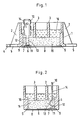
- Fig. 1 einen Schnitt durch die Breitseite eines Stromrichtermoduls,-Fig. 2 einen Schnitt durch die Schmalseite des Moduls.
- Fig. 1 shows a section through the broad side of a converter module, 2 shows a section through the narrow side of the module.
In Fig. 1 ist ein Schnitt durch die Breitseite des Stromrichtermoduls dargestellt. Das Modul besitzt einen oben und unten offenen Rahmen 1, der als Gehäusewandung dient. Der Rahmen 1 weist an seinen beiden Schmalseiten Versteifungskanten 2 auf. Zur Erhöhung der Stabilität besitzt der Rahmen 1 ferner mehrere parallel zur Breitseite bzw. Schmalseite verlaufende Rippen 3. Beim Stromrichtermodul des Ausführungsbeispiels verlaufen zwei Rippen 3 parallel zur Breitseite und zwei Rippen 3 parallel zur Schmalseite. Hierdurch ergeben sich neun rechteckförmige Zellen zur Aufnahme von externen Anschlußelementen für das Modul. Die Rippen 3 dienen gleichzeitig als Isolation und Kriechwegverlängerung zwischen den externen Anschlußelementen. Der Rahmen 1 weist an seinen beiden Schmalseiten in Höhe der Bodenfläche Befestigungslaschen 4 auf. Diese Befestigungslaschen 4 sind mit Bohrungen bzw. U-förmigen Ausnehmungen 5 zur Montage des Stromrichtermoduls auf einem Kühlkörper versehen.1 shows a section through the broad side of the converter module. The module has a
Das Gehäuse des Stromrichtermoduls wird zum einen durch den Rahmen 1, zum anderen durch eine in eine Vertiefung der Bodenfläche des offenen Rahmens 1 aufgesetzte Keramikplatte 6 gebildet. Die Keramikplatte 6 weist Metallisierungen 7 auf ihrer dem Gehäuseinneren zugewandten Fläche auf. Diese Metallisierungen 7 werden beispielsweise durch Kupferfolie realisiert, die gemäß dem aus der Patentanmeldung P 30 36 128.5 bekannten Verfahren direkt ohne Zwischenschicht auf die Keramik aufgebracht sind. Die Metallisierungen 7 dienen als Leiterbahnen und Kontaktflächen zum Auflöten von Anschlußelementen, Halbleiterbauelementen und internen Verbindungslaschen.The housing of the converter module is formed on the one hand by the
Zur mechanischen Stabilisierung der Keramikplatte 6 ist eine dicke Kupferfolie 8 ebenfalls gemäß dem Verfahren nach Patentanmeldung P 30 26 128.5 direkt auf die dem Gehäuseinneren abgewandten Seite der Keramikplatte 6 aufgebracht. Die Stärke der Kupferfolie 8 entspricht ungefähr der Stärke der Metallisierungen 7 (vorzugsweise ebenfalls Kupferfolien). Dadurch werden Verspannungen, die sich infolge der Herstellprozesse und der einseitigen Lötprozesse auf der dem Gehäuseinneren zugewandten Seite der Keramikplatte 6 ergeben, wirksam verhindert. Desweiteren ermöglicht die Kupferfolie 8 einen guten Wärmekontakt zu einem mit dem Modul verbundenen Kühlkörper. Auch ist die Gefahr'von Keramikbrüchen infolge unebener und verschmutzter (Staubkörner) Kühlkörper wesentlich geringer.To mechanically stabilize the
Der Rahmen 1 und die Keramikplatte 6 werden miteinander verklebt. Zur genauen Fixierung der Platte 6 weist der Rahmen 1 die bereits erwähnte umlaufende Vertiefung in seiner Bodenfläche auf, deren Tiefe ungefähr der Dicke der Keramikplatte 6 entspricht. Eine in dieser Vertiefung des Rahmens 1 vorgesehene umlaufende Nut 9 dient dabei zur Aufnahme von austretendem Klebstoff. Der überschüssige Klebstoff wandert in die Nut 9 und quillt nicht über den Rand der Keramikplatte 6 auf die Kühlfläche. Eine mit herausquellendem Klebstoff verschmutzte Kühlfläche der Keramikplatte 6 müßte in nachteiliger Weise zusätzlich bearbeitet werden, um die Klebstoffi reste zu entfernen. Anderenfalls wäre der Wärmeübergang zum Kühlkörper behindert.The
Mit der Metallisierung 7 ist ein Flachstecker 10 als Anschlußelement für einen externen Steckkontakt verlötet. In den Figuren 1 und 2 ist nur ein Flachstecker dargestellt, das Modul des Ausführungsbeispieles kann jedoch insgesamt bis zu neun derartige Flachstecker aufweisen. Der Flachstecker 10 ist auf der Oberseite des Gehäuses frei zugänglich. Er besitzt ein verbreitertes Fußteil 11 zur mechanischen Stabilisierung der Lötstelle auf der Metallisierung 7. An das verbreiterte Fußteil 11 schließen sich eine Abwinkelung 12 und daran ein Dehnungsbogen 13 an. Die Ausführungsform der Abwinkelung 12 und des Dehnungsbogens 13 sind insbesondere aus der Fig. 2 ersichtlich. Der Dehnungsbogen 13 geht an seinem oberen Ende in den eigentlichen Steckanschluß 14 mit Einkerbungen 17 über. Der Dehnungsbogen 13 ist in seinem Querschnitt kleiner als die Querschnitte des oberen Steckanschlusses 14 und des unteren Fußteiles 11. Der Dehnungsbogen 13 vermeidet hohe zyklische Zugspannungen auf die Lötverbindung zwischen Fußteil 11 und Metallisierung 7 der Keramikplatte 6.A
Das mit der Keramikplatte 6 verklebte und mit Halbleiterbauteilen und Flachsteckern bestückte Gehäuse wird in seinem unteren Teil mit einer weichen Vergußmasse (z.B. Silikonkautschuk) 15 zum Schutz der empfindlichen Aktivteile vergossen und zwar sollte der Dehnungsbogen 13 des Flachsteckers 10 voll mit Silikonkautschuk 15 vergossen sein. Das Verschließen des Gehäuses bis knapp über die Gehäusemitte erfolgt mit einer harten Vergußmasse 16 (z.B. Epoxidharz). Durch die harte Vergußmasse 16 werden insbesondere die Flachstecker 10 an ihren Einkerbungen 17 mechanisch stabilisiert.The lower part of the housing, which is glued to the
In Fig. 2 ist ein Schnitt durch die Schmalseite des Stromrichtermoduls dargestellt. Es sind insbesondere der Rahmen 1 mit den Rippen 3 und der umlaufenden Nut 9 zur Klebstoffrestaufnahme ersichtlich. Die den Gehäuseboden bildende Keramikplatte 6 ist einerseits mit der Metallisierung 7, andererseits mit der Kupferfolie 8 beschichtet. Auf die Metallisierung 7 ist der Flachstecker 10 mit seinem Fußteil 11 verlötet. Das Fußteil 11 geht über die Abwinkelung in den Dehnungsbogen 13 über, an den sich der eigentliche Steckanschluß 14 anschließt. Ferner ist die im unteren Gehäuseteil eingegossene weiche Vergußmasse 15 sowie die im mittleren Gehäuseteil eingegossene harte Vergußmasse 16 dargestellt. Das obere Gehäuseteil bleibt zum externen Anschluß der Flachstecker frei von Vergußmassen.In Fig. 2 is a section through the narrow side of the stream judge module shown. In particular, the
Claims (2)
Priority Applications (1)
| Application Number | Priority Date | Filing Date | Title |
|---|---|---|---|
| AT82105678T ATE26505T1 (en) | 1981-07-11 | 1982-06-26 | POWER CONVERTER MODULE. |
Applications Claiming Priority (2)
| Application Number | Priority Date | Filing Date | Title |
|---|---|---|---|
| DE3127457 | 1981-07-11 | ||
| DE3127457A DE3127457C2 (en) | 1981-07-11 | 1981-07-11 | Converter module |
Publications (3)
| Publication Number | Publication Date |
|---|---|
| EP0069901A2 true EP0069901A2 (en) | 1983-01-19 |
| EP0069901A3 EP0069901A3 (en) | 1984-11-21 |
| EP0069901B1 EP0069901B1 (en) | 1987-04-08 |
Family
ID=6136700
Family Applications (1)
| Application Number | Title | Priority Date | Filing Date |
|---|---|---|---|
| EP82105678A Expired EP0069901B1 (en) | 1981-07-11 | 1982-06-26 | Current rectifier module |
Country Status (4)
| Country | Link |
|---|---|
| US (1) | US4670771A (en) |
| EP (1) | EP0069901B1 (en) |
| AT (1) | ATE26505T1 (en) |
| DE (1) | DE3127457C2 (en) |
Cited By (10)
| Publication number | Priority date | Publication date | Assignee | Title |
|---|---|---|---|---|
| EP0118022A2 (en) * | 1983-03-04 | 1984-09-12 | BROWN, BOVERI & CIE Aktiengesellschaft | Rectifier module with fastening part |
| EP0144866A2 (en) * | 1983-11-25 | 1985-06-19 | Kabushiki Kaisha Toshiba | Semiconductor device comprising a substrate |
| EP0155473A1 (en) * | 1984-02-23 | 1985-09-25 | BROWN, BOVERI & CIE Aktiengesellschaft | Power semiconductor module and method of manufacture |
| DE3521572A1 (en) * | 1985-06-15 | 1986-12-18 | Brown, Boveri & Cie Ag, 6800 Mannheim | PERFORMANCE SEMICONDUCTOR MODULE WITH CERAMIC SUBSTRATE |
| EP0237739A2 (en) * | 1986-02-15 | 1987-09-23 | Asea Brown Boveri Aktiengesellschaft | Semiconductor power module and method of producing the module |
| EP0243637A2 (en) * | 1986-03-26 | 1987-11-04 | Asea Brown Boveri Aktiengesellschaft | Semi-conductor power module |
| EP0398108A1 (en) * | 1989-05-13 | 1990-11-22 | Asea Brown Boveri Aktiengesellschaft | Plastic housing and semiconductor power module having this housing |
| FR2668302A1 (en) * | 1990-10-17 | 1992-04-24 | Nec Corp | Housing including one or more integrated circuits and method of manufacturing this housing |
| EP0650191A1 (en) * | 1991-02-20 | 1995-04-26 | Nec Corporation | Structure of semiconductor IC chip |
| DE19615481C5 (en) * | 1996-04-03 | 2013-03-14 | Curamik Electronics Gmbh | Arched metal-ceramic substrate |
Families Citing this family (22)
| Publication number | Priority date | Publication date | Assignee | Title |
|---|---|---|---|---|
| DE3604075A1 (en) * | 1986-02-08 | 1987-08-13 | Bosch Gmbh Robert | Packaging of power components |
| DE3604313A1 (en) * | 1986-02-12 | 1987-08-13 | Bbc Brown Boveri & Cie | Power semiconductor module |
| DE3621994A1 (en) * | 1986-07-01 | 1988-01-14 | Bbc Brown Boveri & Cie | PERFORMANCE SEMICONDUCTOR MODULE |
| DE8703604U1 (en) * | 1987-03-11 | 1988-07-21 | Euroatlas Gmbh Fuer Umformertechnik Und Optronik, 2800 Bremen, De | |
| DE3717489A1 (en) * | 1987-05-23 | 1988-12-01 | Asea Brown Boveri | PERFORMANCE SEMICONDUCTOR MODULE AND METHOD FOR PRODUCING THE MODULE |
| US4739449A (en) * | 1987-06-30 | 1988-04-19 | Kaufman Lance R | Circuit package with thermal expansion relief chimney |
| DE3728096C1 (en) * | 1987-07-03 | 1989-01-12 | Duerrwaechter E Dr Doduco | Flat body, especially for use as a heat sink for electronic power components |
| US5027255A (en) * | 1988-10-22 | 1991-06-25 | Westinghouse Electric Co. | High performance, high current miniaturized low voltage power supply |
| DE3837920A1 (en) * | 1988-11-09 | 1990-05-10 | Semikron Elektronik Gmbh | SEMICONDUCTOR ELEMENT |
| DE3900512A1 (en) * | 1989-01-10 | 1990-07-19 | Tucker Gmbh Bostik | Semiconductor component for a switched-mode power supply |
| DE4001554A1 (en) * | 1990-01-20 | 1991-07-25 | Abb Ixys Semiconductor Gmbh | Power semiconductor module with plastics casing - has deposition struts for ceramic substrate at points away from edge |
| US5243217A (en) * | 1990-11-03 | 1993-09-07 | Fuji Electric Co., Ltd. | Sealed semiconductor device with protruding portion |
| JP2850606B2 (en) * | 1991-11-25 | 1999-01-27 | 富士電機株式会社 | Transistor module |
| AT406434B (en) * | 1993-12-23 | 2000-05-25 | Ixys Semiconductor Gmbh | DEVICE FOR FORMING A THREE-PHASE VOLTAGE SYSTEM INTO A PREDIBLE DC VOLTAGE SUPPLYING A CONSUMER |
| DE4446527A1 (en) * | 1994-12-24 | 1996-06-27 | Ixys Semiconductor Gmbh | Power semiconductor module |
| JP3206717B2 (en) * | 1996-04-02 | 2001-09-10 | 富士電機株式会社 | Power semiconductor module |
| DE19725843C1 (en) * | 1997-06-18 | 1998-10-29 | Siemens Matsushita Components | Aluminium-electrolyte capacitor for AC operation |
| DE19818036B4 (en) * | 1998-04-22 | 2005-05-19 | Siemens Ag | Method for producing an electrotechnical component with a plastic-passivated surface, such component and application of this component |
| JP5745410B2 (en) * | 2008-09-10 | 2015-07-08 | ハートウェア、インコーポレイテッド | TET system for implantable medical devices |
| US8847328B1 (en) | 2013-03-08 | 2014-09-30 | Ixys Corporation | Module and assembly with dual DC-links for three-level NPC applications |
| US9620877B2 (en) | 2014-06-17 | 2017-04-11 | Semiconductor Components Industries, Llc | Flexible press fit pins for semiconductor packages and related methods |
| US9431311B1 (en) | 2015-02-19 | 2016-08-30 | Semiconductor Components Industries, Llc | Semiconductor package with elastic coupler and related methods |
Citations (2)
| Publication number | Priority date | Publication date | Assignee | Title |
|---|---|---|---|---|
| DE2840514A1 (en) * | 1977-09-19 | 1979-03-22 | Gentron Corp | POWER CONTROL UNIT AND METHOD OF ATTACHING THESE |
| DE2819327A1 (en) * | 1978-05-03 | 1979-12-13 | Semikron Gleichrichterbau | SEMI-CONDUCTOR UNIT |
Family Cites Families (12)
| Publication number | Priority date | Publication date | Assignee | Title |
|---|---|---|---|---|
| US3265805A (en) * | 1964-02-03 | 1966-08-09 | Power Components Inc | Semiconductor power device |
| US3370207A (en) * | 1964-02-24 | 1968-02-20 | Gen Electric | Multilayer contact system for semiconductor devices including gold and copper layers |
| DE1564749A1 (en) * | 1966-10-27 | 1970-01-08 | Semikron Gleichrichterbau | Semiconductor device |
| US3475662A (en) * | 1967-11-22 | 1969-10-28 | Westinghouse Electric Corp | Hermetically sealed electrical device |
| US3829598A (en) * | 1972-09-25 | 1974-08-13 | Hutson Ind Inc | Copper heat sinks for electronic devices and method of making same |
| US3994430A (en) * | 1975-07-30 | 1976-11-30 | General Electric Company | Direct bonding of metals to ceramics and metals |
| JPS5315763A (en) * | 1976-07-28 | 1978-02-14 | Hitachi Ltd | Resin sealed type semiconductor device |
| US4117508A (en) * | 1977-03-21 | 1978-09-26 | General Electric Company | Pressurizable semiconductor pellet assembly |
| US4249034A (en) * | 1978-11-27 | 1981-02-03 | General Electric Company | Semiconductor package having strengthening and sealing upper chamber |
| DE3028178C2 (en) * | 1980-07-25 | 1985-05-09 | Brown, Boveri & Cie Ag, 6800 Mannheim | Power semiconductor module |
| DE3036128C2 (en) * | 1980-09-25 | 1983-08-18 | Brown, Boveri & Cie Ag, 6800 Mannheim | Process for direct bonding of copper foils to oxide ceramic substrates |
| US4514587A (en) * | 1981-12-23 | 1985-04-30 | Unitrode Corporation | High power semiconductor package |
-
1981
- 1981-07-11 DE DE3127457A patent/DE3127457C2/en not_active Expired
-
1982
- 1982-06-26 AT AT82105678T patent/ATE26505T1/en not_active IP Right Cessation
- 1982-06-26 EP EP82105678A patent/EP0069901B1/en not_active Expired
-
1985
- 1985-08-02 US US06/762,802 patent/US4670771A/en not_active Expired - Lifetime
Patent Citations (2)
| Publication number | Priority date | Publication date | Assignee | Title |
|---|---|---|---|---|
| DE2840514A1 (en) * | 1977-09-19 | 1979-03-22 | Gentron Corp | POWER CONTROL UNIT AND METHOD OF ATTACHING THESE |
| DE2819327A1 (en) * | 1978-05-03 | 1979-12-13 | Semikron Gleichrichterbau | SEMI-CONDUCTOR UNIT |
Cited By (16)
| Publication number | Priority date | Publication date | Assignee | Title |
|---|---|---|---|---|
| EP0118022A3 (en) * | 1983-03-04 | 1985-11-06 | Brown, Boveri & Cie Aktiengesellschaft | Rectifier module with fastening part |
| EP0118022A2 (en) * | 1983-03-04 | 1984-09-12 | BROWN, BOVERI & CIE Aktiengesellschaft | Rectifier module with fastening part |
| EP0144866A2 (en) * | 1983-11-25 | 1985-06-19 | Kabushiki Kaisha Toshiba | Semiconductor device comprising a substrate |
| EP0144866B1 (en) * | 1983-11-25 | 1988-09-07 | Kabushiki Kaisha Toshiba | Semiconductor device comprising a substrate |
| EP0155473A1 (en) * | 1984-02-23 | 1985-09-25 | BROWN, BOVERI & CIE Aktiengesellschaft | Power semiconductor module and method of manufacture |
| DE3521572A1 (en) * | 1985-06-15 | 1986-12-18 | Brown, Boveri & Cie Ag, 6800 Mannheim | PERFORMANCE SEMICONDUCTOR MODULE WITH CERAMIC SUBSTRATE |
| EP0205746A2 (en) * | 1985-06-15 | 1986-12-30 | Asea Brown Boveri Aktiengesellschaft | Semiconductor power module comprising a ceramic substrate |
| EP0205746A3 (en) * | 1985-06-15 | 1987-07-22 | Brown, Boveri & Cie Aktiengesellschaft | Semiconductor power module comprising a ceramic substrate |
| EP0237739A3 (en) * | 1986-02-15 | 1989-03-15 | Asea Brown Boveri Aktiengesellschaft | Semiconductor power module and method of producing the module |
| EP0237739A2 (en) * | 1986-02-15 | 1987-09-23 | Asea Brown Boveri Aktiengesellschaft | Semiconductor power module and method of producing the module |
| EP0243637A2 (en) * | 1986-03-26 | 1987-11-04 | Asea Brown Boveri Aktiengesellschaft | Semi-conductor power module |
| EP0243637A3 (en) * | 1986-03-26 | 1990-05-16 | Asea Brown Boveri Aktiengesellschaft | Semi-conductor power module |
| EP0398108A1 (en) * | 1989-05-13 | 1990-11-22 | Asea Brown Boveri Aktiengesellschaft | Plastic housing and semiconductor power module having this housing |
| FR2668302A1 (en) * | 1990-10-17 | 1992-04-24 | Nec Corp | Housing including one or more integrated circuits and method of manufacturing this housing |
| EP0650191A1 (en) * | 1991-02-20 | 1995-04-26 | Nec Corporation | Structure of semiconductor IC chip |
| DE19615481C5 (en) * | 1996-04-03 | 2013-03-14 | Curamik Electronics Gmbh | Arched metal-ceramic substrate |
Also Published As
| Publication number | Publication date |
|---|---|
| ATE26505T1 (en) | 1987-04-15 |
| EP0069901A3 (en) | 1984-11-21 |
| DE3127457A1 (en) | 1983-02-03 |
| EP0069901B1 (en) | 1987-04-08 |
| US4670771A (en) | 1987-06-02 |
| DE3127457C2 (en) | 1985-09-12 |
Similar Documents
| Publication | Publication Date | Title |
|---|---|---|
| EP0069901B1 (en) | Current rectifier module | |
| DE10149580B4 (en) | Semiconductor device | |
| DE19601372B4 (en) | Semiconductor module | |
| DE10031678C2 (en) | power module | |
| DE19921109B4 (en) | Electronic component and electronic component with a ceramic component element | |
| DE19941872B4 (en) | Electronic component, e.g. an acoustic surface acoustic wave device, and methods of manufacturing the same | |
| DE102006037118B3 (en) | Semiconductor switching module for vehicle electrical systems with a plurality of semiconductor chips, use of such a semiconductor switching module and method for producing the same | |
| EP0111659B1 (en) | Power transistor module | |
| DE3241508C2 (en) | ||
| DE19625240A1 (en) | Semiconductor intelligent power module device for e.g. IGBT | |
| DE3221199A1 (en) | ISOLATED TYPE SEMICONDUCTOR ARRANGEMENT | |
| DE19518753A1 (en) | Semiconductor device having high reliability | |
| DE102005049687A1 (en) | Power semiconductor component in flat conductor technology with vertical current path | |
| DE10222608B4 (en) | Semiconductor device and method for manufacturing the same | |
| EP0292848B1 (en) | Semiconductor power module and method of manufacturing it | |
| DE102016203581A1 (en) | SEMICONDUCTOR DEVICE AND METHOD FOR PRODUCING A SEMICONDUCTOR DEVICE | |
| DE69923374T2 (en) | Semiconductor device | |
| DE212018000073U1 (en) | Semiconductor device | |
| DE102014104856A1 (en) | Explosion-proof power semiconductor module | |
| CH663491A5 (en) | Electronic circuit module | |
| DE10221857A1 (en) | Process for applying a semiconductor chip on a thermal and/or electrically conducting connecting part arranged in or on a plastic housing body comprises using a soft soldering process | |
| DE3243689C2 (en) | ||
| DE2937051A1 (en) | FLAT PACKAGE FOR RECEIVING ELECTRICAL MICROCIRCUITS AND METHOD FOR THE PRODUCTION THEREOF | |
| EP1595287B1 (en) | Electronic component comprising a semiconductor chip and method for producing said component | |
| EP1324386A1 (en) | Semiconductor module and method of manufacturing a semiconductor module |
Legal Events
| Date | Code | Title | Description |
|---|---|---|---|
| PUAI | Public reference made under article 153(3) epc to a published international application that has entered the european phase |
Free format text: ORIGINAL CODE: 0009012 |
|
| AK | Designated contracting states |
Designated state(s): AT FR GB IT NL SE |
|
| PUAL | Search report despatched |
Free format text: ORIGINAL CODE: 0009013 |
|
| AK | Designated contracting states |
Designated state(s): AT FR GB IT NL SE |
|
| 17P | Request for examination filed |
Effective date: 19841201 |
|
| 17Q | First examination report despatched |
Effective date: 19860225 |
|
| GRAA | (expected) grant |
Free format text: ORIGINAL CODE: 0009210 |
|
| AK | Designated contracting states |
Kind code of ref document: B1 Designated state(s): AT FR GB IT NL SE |
|
| REF | Corresponds to: |
Ref document number: 26505 Country of ref document: AT Date of ref document: 19870415 Kind code of ref document: T |
|
| ET | Fr: translation filed | ||
| ITF | It: translation for a ep patent filed |
Owner name: DE DOMINICIS & MAYER S.R.L. |
|
| PLBE | No opposition filed within time limit |
Free format text: ORIGINAL CODE: 0009261 |
|
| STAA | Information on the status of an ep patent application or granted ep patent |
Free format text: STATUS: NO OPPOSITION FILED WITHIN TIME LIMIT |
|
| 26N | No opposition filed | ||
| PGFP | Annual fee paid to national office [announced via postgrant information from national office to epo] |
Ref country code: AT Payment date: 19900425 Year of fee payment: 9 |
|
| PGFP | Annual fee paid to national office [announced via postgrant information from national office to epo] |
Ref country code: SE Payment date: 19900525 Year of fee payment: 9 |
|
| PGFP | Annual fee paid to national office [announced via postgrant information from national office to epo] |
Ref country code: NL Payment date: 19900630 Year of fee payment: 9 |
|
| PG25 | Lapsed in a contracting state [announced via postgrant information from national office to epo] |
Ref country code: AT Effective date: 19910626 |
|
| PG25 | Lapsed in a contracting state [announced via postgrant information from national office to epo] |
Ref country code: SE Effective date: 19910627 |
|
| ITTA | It: last paid annual fee | ||
| PG25 | Lapsed in a contracting state [announced via postgrant information from national office to epo] |
Ref country code: NL Effective date: 19920101 |
|
| NLV4 | Nl: lapsed or anulled due to non-payment of the annual fee | ||
| EUG | Se: european patent has lapsed |
Ref document number: 82105678.5 Effective date: 19920109 |
|
| REG | Reference to a national code |
Ref country code: FR Ref legal event code: TP Ref country code: FR Ref legal event code: CD |
|
| REG | Reference to a national code |
Ref country code: GB Ref legal event code: 732E |
|
| PGFP | Annual fee paid to national office [announced via postgrant information from national office to epo] |
Ref country code: GB Payment date: 20010522 Year of fee payment: 20 |
|
| PGFP | Annual fee paid to national office [announced via postgrant information from national office to epo] |
Ref country code: FR Payment date: 20010621 Year of fee payment: 20 |
|
| REG | Reference to a national code |
Ref country code: GB Ref legal event code: IF02 |
|
| PG25 | Lapsed in a contracting state [announced via postgrant information from national office to epo] |
Ref country code: GB Free format text: LAPSE BECAUSE OF EXPIRATION OF PROTECTION Effective date: 20020625 |
|
| REG | Reference to a national code |
Ref country code: GB Ref legal event code: PE20 Effective date: 20020625 |