EP0069429A2 - Feldeffekttransistor mit isoliertem Gate - Google Patents
Feldeffekttransistor mit isoliertem Gate Download PDFInfo
- Publication number
- EP0069429A2 EP0069429A2 EP82200826A EP82200826A EP0069429A2 EP 0069429 A2 EP0069429 A2 EP 0069429A2 EP 82200826 A EP82200826 A EP 82200826A EP 82200826 A EP82200826 A EP 82200826A EP 0069429 A2 EP0069429 A2 EP 0069429A2
- Authority
- EP
- European Patent Office
- Prior art keywords
- zone
- drain
- epitaxial layer
- semiconductor device
- effect transistor
- Prior art date
- Legal status (The legal status is an assumption and is not a legal conclusion. Google has not performed a legal analysis and makes no representation as to the accuracy of the status listed.)
- Granted
Links
- 230000005669 field effect Effects 0.000 title claims abstract description 33
- 239000004065 semiconductor Substances 0.000 claims abstract description 33
- 239000000758 substrate Substances 0.000 claims abstract description 16
- 230000015556 catabolic process Effects 0.000 claims description 19
- 230000000295 complement effect Effects 0.000 claims description 3
- 239000004020 conductor Substances 0.000 claims description 3
- 108091006146 Channels Proteins 0.000 description 8
- 238000000034 method Methods 0.000 description 6
- 229910052751 metal Inorganic materials 0.000 description 5
- 239000002184 metal Substances 0.000 description 5
- 238000010276 construction Methods 0.000 description 3
- 239000000463 material Substances 0.000 description 3
- 229910052710 silicon Inorganic materials 0.000 description 3
- 239000010703 silicon Substances 0.000 description 3
- 238000009792 diffusion process Methods 0.000 description 2
- 229910021420 polycrystalline silicon Inorganic materials 0.000 description 2
- 238000006677 Appel reaction Methods 0.000 description 1
- JBRZTFJDHDCESZ-UHFFFAOYSA-N AsGa Chemical compound [As]#[Ga] JBRZTFJDHDCESZ-UHFFFAOYSA-N 0.000 description 1
- 229910001218 Gallium arsenide Inorganic materials 0.000 description 1
- 102000004129 N-Type Calcium Channels Human genes 0.000 description 1
- 108090000699 N-Type Calcium Channels Proteins 0.000 description 1
- VYPSYNLAJGMNEJ-UHFFFAOYSA-N Silicium dioxide Chemical compound O=[Si]=O VYPSYNLAJGMNEJ-UHFFFAOYSA-N 0.000 description 1
- 150000001875 compounds Chemical class 0.000 description 1
- 230000007423 decrease Effects 0.000 description 1
- 230000001419 dependent effect Effects 0.000 description 1
- 238000010586 diagram Methods 0.000 description 1
- 230000000694 effects Effects 0.000 description 1
- 238000005516 engineering process Methods 0.000 description 1
- 230000002349 favourable effect Effects 0.000 description 1
- 229910052732 germanium Inorganic materials 0.000 description 1
- GNPVGFCGXDBREM-UHFFFAOYSA-N germanium atom Chemical compound [Ge] GNPVGFCGXDBREM-UHFFFAOYSA-N 0.000 description 1
- 238000007689 inspection Methods 0.000 description 1
- 238000005468 ion implantation Methods 0.000 description 1
- 230000000750 progressive effect Effects 0.000 description 1
- 238000000926 separation method Methods 0.000 description 1
- 229910052814 silicon oxide Inorganic materials 0.000 description 1
Images


Classifications
-
- H—ELECTRICITY
- H01—ELECTRIC ELEMENTS
- H01L—SEMICONDUCTOR DEVICES NOT COVERED BY CLASS H10
- H01L29/00—Semiconductor devices adapted for rectifying, amplifying, oscillating or switching, or capacitors or resistors with at least one potential-jump barrier or surface barrier, e.g. PN junction depletion layer or carrier concentration layer; Details of semiconductor bodies or of electrodes thereof ; Multistep manufacturing processes therefor
- H01L29/40—Electrodes ; Multistep manufacturing processes therefor
- H01L29/41—Electrodes ; Multistep manufacturing processes therefor characterised by their shape, relative sizes or dispositions
- H01L29/417—Electrodes ; Multistep manufacturing processes therefor characterised by their shape, relative sizes or dispositions carrying the current to be rectified, amplified or switched
- H01L29/41725—Source or drain electrodes for field effect devices
- H01L29/41775—Source or drain electrodes for field effect devices characterised by the proximity or the relative position of the source or drain electrode and the gate electrode, e.g. the source or drain electrode separated from the gate electrode by side-walls or spreading around or above the gate electrode
-
- H—ELECTRICITY
- H01—ELECTRIC ELEMENTS
- H01L—SEMICONDUCTOR DEVICES NOT COVERED BY CLASS H10
- H01L29/00—Semiconductor devices adapted for rectifying, amplifying, oscillating or switching, or capacitors or resistors with at least one potential-jump barrier or surface barrier, e.g. PN junction depletion layer or carrier concentration layer; Details of semiconductor bodies or of electrodes thereof ; Multistep manufacturing processes therefor
- H01L29/02—Semiconductor bodies ; Multistep manufacturing processes therefor
- H01L29/06—Semiconductor bodies ; Multistep manufacturing processes therefor characterised by their shape; characterised by the shapes, relative sizes, or dispositions of the semiconductor regions ; characterised by the concentration or distribution of impurities within semiconductor regions
- H01L29/10—Semiconductor bodies ; Multistep manufacturing processes therefor characterised by their shape; characterised by the shapes, relative sizes, or dispositions of the semiconductor regions ; characterised by the concentration or distribution of impurities within semiconductor regions with semiconductor regions connected to an electrode not carrying current to be rectified, amplified or switched and such electrode being part of a semiconductor device which comprises three or more electrodes
- H01L29/107—Substrate region of field-effect devices
- H01L29/1075—Substrate region of field-effect devices of field-effect transistors
- H01L29/1079—Substrate region of field-effect devices of field-effect transistors with insulated gate
- H01L29/1083—Substrate region of field-effect devices of field-effect transistors with insulated gate with an inactive supplementary region, e.g. for preventing punch-through, improving capacity effect or leakage current
-
- H—ELECTRICITY
- H01—ELECTRIC ELEMENTS
- H01L—SEMICONDUCTOR DEVICES NOT COVERED BY CLASS H10
- H01L29/00—Semiconductor devices adapted for rectifying, amplifying, oscillating or switching, or capacitors or resistors with at least one potential-jump barrier or surface barrier, e.g. PN junction depletion layer or carrier concentration layer; Details of semiconductor bodies or of electrodes thereof ; Multistep manufacturing processes therefor
- H01L29/40—Electrodes ; Multistep manufacturing processes therefor
- H01L29/402—Field plates
- H01L29/404—Multiple field plate structures
-
- H—ELECTRICITY
- H01—ELECTRIC ELEMENTS
- H01L—SEMICONDUCTOR DEVICES NOT COVERED BY CLASS H10
- H01L29/00—Semiconductor devices adapted for rectifying, amplifying, oscillating or switching, or capacitors or resistors with at least one potential-jump barrier or surface barrier, e.g. PN junction depletion layer or carrier concentration layer; Details of semiconductor bodies or of electrodes thereof ; Multistep manufacturing processes therefor
- H01L29/40—Electrodes ; Multistep manufacturing processes therefor
- H01L29/41—Electrodes ; Multistep manufacturing processes therefor characterised by their shape, relative sizes or dispositions
- H01L29/417—Electrodes ; Multistep manufacturing processes therefor characterised by their shape, relative sizes or dispositions carrying the current to be rectified, amplified or switched
- H01L29/41725—Source or drain electrodes for field effect devices
- H01L29/41758—Source or drain electrodes for field effect devices for lateral devices with structured layout for source or drain region, i.e. the source or drain region having cellular, interdigitated or ring structure or being curved or angular
-
- H—ELECTRICITY
- H01—ELECTRIC ELEMENTS
- H01L—SEMICONDUCTOR DEVICES NOT COVERED BY CLASS H10
- H01L29/00—Semiconductor devices adapted for rectifying, amplifying, oscillating or switching, or capacitors or resistors with at least one potential-jump barrier or surface barrier, e.g. PN junction depletion layer or carrier concentration layer; Details of semiconductor bodies or of electrodes thereof ; Multistep manufacturing processes therefor
- H01L29/40—Electrodes ; Multistep manufacturing processes therefor
- H01L29/41—Electrodes ; Multistep manufacturing processes therefor characterised by their shape, relative sizes or dispositions
- H01L29/423—Electrodes ; Multistep manufacturing processes therefor characterised by their shape, relative sizes or dispositions not carrying the current to be rectified, amplified or switched
- H01L29/42312—Gate electrodes for field effect devices
- H01L29/42316—Gate electrodes for field effect devices for field-effect transistors
- H01L29/4232—Gate electrodes for field effect devices for field-effect transistors with insulated gate
- H01L29/42364—Gate electrodes for field effect devices for field-effect transistors with insulated gate characterised by the insulating layer, e.g. thickness or uniformity
- H01L29/42368—Gate electrodes for field effect devices for field-effect transistors with insulated gate characterised by the insulating layer, e.g. thickness or uniformity the thickness being non-uniform
-
- H—ELECTRICITY
- H01—ELECTRIC ELEMENTS
- H01L—SEMICONDUCTOR DEVICES NOT COVERED BY CLASS H10
- H01L29/00—Semiconductor devices adapted for rectifying, amplifying, oscillating or switching, or capacitors or resistors with at least one potential-jump barrier or surface barrier, e.g. PN junction depletion layer or carrier concentration layer; Details of semiconductor bodies or of electrodes thereof ; Multistep manufacturing processes therefor
- H01L29/66—Types of semiconductor device ; Multistep manufacturing processes therefor
- H01L29/68—Types of semiconductor device ; Multistep manufacturing processes therefor controllable by only the electric current supplied, or only the electric potential applied, to an electrode which does not carry the current to be rectified, amplified or switched
- H01L29/76—Unipolar devices, e.g. field effect transistors
- H01L29/772—Field effect transistors
- H01L29/78—Field effect transistors with field effect produced by an insulated gate
- H01L29/7833—Field effect transistors with field effect produced by an insulated gate with lightly doped drain or source extension, e.g. LDD MOSFET's; DDD MOSFET's
- H01L29/7835—Field effect transistors with field effect produced by an insulated gate with lightly doped drain or source extension, e.g. LDD MOSFET's; DDD MOSFET's with asymmetrical source and drain regions, e.g. lateral high-voltage MISFETs with drain offset region, extended drain MISFETs
-
- H—ELECTRICITY
- H01—ELECTRIC ELEMENTS
- H01L—SEMICONDUCTOR DEVICES NOT COVERED BY CLASS H10
- H01L29/00—Semiconductor devices adapted for rectifying, amplifying, oscillating or switching, or capacitors or resistors with at least one potential-jump barrier or surface barrier, e.g. PN junction depletion layer or carrier concentration layer; Details of semiconductor bodies or of electrodes thereof ; Multistep manufacturing processes therefor
- H01L29/02—Semiconductor bodies ; Multistep manufacturing processes therefor
- H01L29/06—Semiconductor bodies ; Multistep manufacturing processes therefor characterised by their shape; characterised by the shapes, relative sizes, or dispositions of the semiconductor regions ; characterised by the concentration or distribution of impurities within semiconductor regions
- H01L29/0603—Semiconductor bodies ; Multistep manufacturing processes therefor characterised by their shape; characterised by the shapes, relative sizes, or dispositions of the semiconductor regions ; characterised by the concentration or distribution of impurities within semiconductor regions characterised by particular constructional design considerations, e.g. for preventing surface leakage, for controlling electric field concentration or for internal isolations regions
- H01L29/0607—Semiconductor bodies ; Multistep manufacturing processes therefor characterised by their shape; characterised by the shapes, relative sizes, or dispositions of the semiconductor regions ; characterised by the concentration or distribution of impurities within semiconductor regions characterised by particular constructional design considerations, e.g. for preventing surface leakage, for controlling electric field concentration or for internal isolations regions for preventing surface leakage or controlling electric field concentration
- H01L29/0611—Semiconductor bodies ; Multistep manufacturing processes therefor characterised by their shape; characterised by the shapes, relative sizes, or dispositions of the semiconductor regions ; characterised by the concentration or distribution of impurities within semiconductor regions characterised by particular constructional design considerations, e.g. for preventing surface leakage, for controlling electric field concentration or for internal isolations regions for preventing surface leakage or controlling electric field concentration for increasing or controlling the breakdown voltage of reverse biased devices
- H01L29/0615—Semiconductor bodies ; Multistep manufacturing processes therefor characterised by their shape; characterised by the shapes, relative sizes, or dispositions of the semiconductor regions ; characterised by the concentration or distribution of impurities within semiconductor regions characterised by particular constructional design considerations, e.g. for preventing surface leakage, for controlling electric field concentration or for internal isolations regions for preventing surface leakage or controlling electric field concentration for increasing or controlling the breakdown voltage of reverse biased devices by the doping profile or the shape or the arrangement of the PN junction, or with supplementary regions, e.g. junction termination extension [JTE]
- H01L29/063—Reduced surface field [RESURF] pn-junction structures
-
- H—ELECTRICITY
- H01—ELECTRIC ELEMENTS
- H01L—SEMICONDUCTOR DEVICES NOT COVERED BY CLASS H10
- H01L29/00—Semiconductor devices adapted for rectifying, amplifying, oscillating or switching, or capacitors or resistors with at least one potential-jump barrier or surface barrier, e.g. PN junction depletion layer or carrier concentration layer; Details of semiconductor bodies or of electrodes thereof ; Multistep manufacturing processes therefor
- H01L29/02—Semiconductor bodies ; Multistep manufacturing processes therefor
- H01L29/06—Semiconductor bodies ; Multistep manufacturing processes therefor characterised by their shape; characterised by the shapes, relative sizes, or dispositions of the semiconductor regions ; characterised by the concentration or distribution of impurities within semiconductor regions
- H01L29/0684—Semiconductor bodies ; Multistep manufacturing processes therefor characterised by their shape; characterised by the shapes, relative sizes, or dispositions of the semiconductor regions ; characterised by the concentration or distribution of impurities within semiconductor regions characterised by the shape, relative sizes or dispositions of the semiconductor regions or junctions between the regions
- H01L29/0692—Surface layout
-
- H—ELECTRICITY
- H01—ELECTRIC ELEMENTS
- H01L—SEMICONDUCTOR DEVICES NOT COVERED BY CLASS H10
- H01L29/00—Semiconductor devices adapted for rectifying, amplifying, oscillating or switching, or capacitors or resistors with at least one potential-jump barrier or surface barrier, e.g. PN junction depletion layer or carrier concentration layer; Details of semiconductor bodies or of electrodes thereof ; Multistep manufacturing processes therefor
- H01L29/02—Semiconductor bodies ; Multistep manufacturing processes therefor
- H01L29/06—Semiconductor bodies ; Multistep manufacturing processes therefor characterised by their shape; characterised by the shapes, relative sizes, or dispositions of the semiconductor regions ; characterised by the concentration or distribution of impurities within semiconductor regions
- H01L29/08—Semiconductor bodies ; Multistep manufacturing processes therefor characterised by their shape; characterised by the shapes, relative sizes, or dispositions of the semiconductor regions ; characterised by the concentration or distribution of impurities within semiconductor regions with semiconductor regions connected to an electrode carrying current to be rectified, amplified or switched and such electrode being part of a semiconductor device which comprises three or more electrodes
- H01L29/0843—Source or drain regions of field-effect devices
- H01L29/0847—Source or drain regions of field-effect devices of field-effect transistors with insulated gate
Definitions
- the invention relates to a semiconductor device having a semiconductor body comprising a surface-adjoining first region of a first conductivity type in which an insulated gate field effect transitor is provided, having highly doped source and drain zones of the second, opposite conductivity type, a surface zone of the second conductivity type adjoining the drain zone and having a lower doping concentration than the drain zone, said surface zone extending in the direction of the source zone, a channel region of the first conductivity type present between said surface zone and the source zone, and a gate electrode present above the channel region and separated from the channel region by an electrically insulating layer, a field plate being provided between the source and drain zones and extending in the direction of the drain zone to above the said surface zone but not to above the drain zone and being insulated from the semiconductor surface, the said field plate having a connection conductor.
- a semiconductor device of the kind described in the opening paragraph is known from Netherlands Patent Application No. 7713333 laid open to public inspection.
- An improvement of this structure by which disturbing influences of electric charges formed on the insulating layer are reduced is achieved by providing a .field plate which is preferably connected to the source electrode and which extends to above the surface zone but at a distance from the highly doped drain zone.
- a .field plate which is preferably connected to the source electrode and which extends to above the surface zone but at a distance from the highly doped drain zone.
- undesired instabilities may occur as a result of charge fluctuations on the uncovered part of the insulating layer present between the field plate and the highly doped drain zone.
- Oneof the objects of the invention is to provide a semiconductor device having a field effect transistor of a new structure with a high drain breakdown voltage and stable electric properties and which can be used advantageously in integrated circuits and is suitable in particular for use in circuits in which the source and drain zones have a high voltage relative to the substrate, for example in source follower circuits.
- the invention is inter alia based on the recognition of the fact that this object can be achieved by means of a structure in which the said surface zone is pinched off progressively on two sides, that is to say from the top and bottom sides, when the drain voltage increases.
- a semiconductor device of the kind mentioned in the-opening paragraph is characterized according to the invention in that the first region is an epitaxial layer forming with a substrate of the second conductivity type ap-n junction which inoperation is reverse biased, that a buried layer of the first conductivity type having a higher doping concentration than the epitaxial layer is provided between said epitaxial layer and the substrate and below at least the channel region and a part of the surface zone, said buried layer not extending below the drain zone, and that the field plate extends above the surface zone on insulating layer parts of a thickness increasing in the direction of the drain zone as a result of which in the direction of the drain zone successive parts of the surface zone are successively pinched off when the drain voltage increases.
- a progressive, phased, two-sided depletion of said surface zone is ob.tained in the direction from the source zone to the drain zone when the drain voltage increases.
- This phased two-sides depletion occurs between the epitaxial layer and the field plate and can be:obtained even when only one surface zone is used, which can be manufactured in one single doping step.
- the field distribution is favourable influenced by reduction of the surface field strength.
- field plate as meant in this Application may consist of one single conductive layer or of mutually separated subfield plates which, if required, may each individually be contacted.
- the epitaxial layer has such a small doping concentration and thiciness that at least near the drain zone it is depleted throughout its thickness at a drain voltage which is lower than the drain breakdown voltage, all. this according to the so-called "RESURF” principle as described inter alia in Philips Journal of Research, Vol. 35, 1980 pp,1-13. With this construction the highest breakdown voltages are reached.
- the field plate is preferably spaced from the highly doped drain zone in order to avoid breakdown between field plate and drain zone via the insulating layer.
- the field plate is preferably electrically connected to the source electrode or to the gate electrode.
- the thickness of the isolating layer on which the field plate is present may increase continuously in the direction of the drain zone. According to a third embodiment said thickness increases stepwise.
- the highly doped drain zone may be embedded in a part of the lower doped surface zone. As a result of this the influence of the edge curvature of the highly doped drain- zone decreases.
- the doping concentration may increase from the surface zone in the direction of the drain zone, although technologically this is slightly more complicated.
- a further measure to increase the breakdown voltage may be that the drain electrode extends in the direction of the source zone to above the surface zone and thus serves as a field electrode.
- the source zone should have a potential which is substantially equal to that of the epitaxial layer although a difference of a few volts is acceptable.
- the source zone is electrically connected to the epitaxial layer.
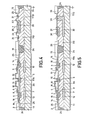
- Fig. 1 is a diagrammatic cross-sectional view of a part of a semiconductor device according to the invention.
- the device comprises a semiconductor body 1, in this example of silicon, having a region 3 of a first conductivity type, in this case the n conductivity type, which adjoins a surface 2 and in which an insulated gate field effect transistor is provided.
- the field effect transistor comprises highly doped source and drain zones 4 and 5 of the second opposite conductivity type, so in this example of the p-type. Furthermore a surface zone 6 of the second E-conductivity type adjoining the drain zone 5 is present having a lower doping concentration thaan the drain zone 5. The surface zone 6 extends in the direction of the source zone 4. Between said zone 6 and the source zone 4 the n-type channel region 7 of the field effect transistor is present which forms part of the region 3. Above the channel region 7 is present a gate electrode 8 of the field effect transistor, which gate electrode is separated from the channel region 7 by an electrically insulating layer, in this example a silicon oxide layer 9.
- the gate electrode 8 in this example is of polycrystalline silicon, but may also be of metal.
- a conductive field plate 10 in this example a metal layer, is provided between the source and drain zones 4 and 5 and extends in the direction of the drain zone 5 to above the surface zone 6 but not to above the drain zone 5.
- the field plate 10 is insulated from the semiconductor surface 2 and is connected via a metal layer 18 to such a potential that the zone 6 is depleted from above when the drain voltage increases.
- this purpose is achieved in that the field plate 10 is connected to the source electrode 16 via the metal layer part 18.
- the source electrode is connected to the region 3 via a highly doped contact zone 14.
- the field plate 10 according to the invention extends above the surface zone 6 on insulating layer parts (13A, 13B) of a thickness increasing in the direction of the drain zone 5.
- successive parts (a, b, c; see fig. 1) of the surface zone 6 are successively pinched off in the direction of the drain zone 5.
- the field distribution is influenced so that the field strength at the surface 2 is optimally reduced.
- higher drain breakdown voltages can be realized than in the known "extended drain” field effect transistors as described in the said Netherlands Patent Application 7713333.
- a higher doping of the zone 6 may be used than in the known structure.
- the field plate 10 need not be connected to the source electrode 16 but, for example as shown in fig. 3, may be connectedinstead thereof to the gate electrode 8. It is of importance that in the operating condition the potentials of the field plate 10 and of the epitaxial layer 3 on both sides of the surface zone 6 should have the same sign relative to said zone so that the zone 6 is two-sided depleted when the drain voltage increases. In order to achieve this the field plate 10 may also be connected, if desired, via a separate connection conductor to a suitable potential.
- the field plate may also consist of separated sub-field plates which are each on a different oxide thickness and are each individually connected to a desired potential.
- the epitaxial layer 3 has such a small doping concentration and thickness that at least near the drain zone it is depleted throughout its thickness at a drain voltage which is lower than the drain breakdown voltage.
- a doping in the order of magnitude of 10 12 doping atoms per cm 2 over the thickness of the layer 3 is generally necessary.
- fig. 5 is a cross-sectional view of a part of an integrated circuit in which a p-channel field effect transistor of the type shown in fig. 3, in this case again considered to be symmetrical with respect to the dram electrode 5, is present in the first island-shaped part 3A of the epitaxial layer 3, and that a bipolar transistor is provided in an adjacent second island-shaped part 3B.
- Corresponding parts of the field effect transistors are referred to by the same reference numerals in figs. 1 to 5.
- the bipolar transistor is a vertical nnn-transistor having an n-type emitter zone 30 and a p-type base zone 31, the collector zone of which transistor is formed by the island 3B and the n-type buried layer 32 which is contacted at the surface via a diffused n-type connection zone 33.
- the emitter zone 30 may be formed simultaneously with the zones 14 and the base zone 31 may be formed simultaneously with the zones 4 and 5.
- Fig. 7 is a diagrammatic plan view and fig. 8 is a diagrammatic cross-sectional view taken on.the line VIII-VIII of a field effect transistor structure in accordance with the invention having a U-shaped geometry.
- the field plate 10 is connected to the gate electrode 8.-
- the device is of the type shown in Fig. 3.
- the substrate 11 is of p-type silicon having a resistivity of 30 Ohm.cm.
- the n-type epitaxial layer 3 has a resistivity of approximately 4 Ohm. cm and a thickness of approximately 15 / um.
- the buried n-type layer 12 has a spacing of approximately 10 / um to the surface 2.
- the surface zone 6 has a thickness of approximately 2 / um and an overall doping of 1.8 x 10 12 atoms per cm 2 ; this zone is preferably made by ion implantation. Otherwise the semiconductor devices shown in figs. 1 to 5, 7 and 8 can all be manufactured by means of different methods usual in semiconductor technology.
- the field effect transistor shown in figs. 7 and 8 uses two-sided depletion of the epitaxial layer 3 and can operate at drain voltages up to 250 Volts and higher.
- the field plate 10 is present on an oxide layer 13 with only one step; in order to reach an even better phased pinching of the surface zone 6 the number of steps may be increased at will.
- the invention is not limited to the examples described.
- the conductivity types mentioned in the examples may all be replaced simultaneously by their opposite ones.
- the materials for the conductive and insulating layers may also be replaced by other ones, while as a semiconductor material other semiconductor materials, for example germanium or A III B V compounds, for example gallium arsenide, may be used instead of silicon.
Applications Claiming Priority (2)
| Application Number | Priority Date | Filing Date | Title |
|---|---|---|---|
| NL8103218A NL8103218A (nl) | 1981-07-06 | 1981-07-06 | Veldeffekttransistor met geisoleerde stuurelektrode. |
| NL8103218 | 1981-07-06 |
Publications (3)
| Publication Number | Publication Date |
|---|---|
| EP0069429A2 true EP0069429A2 (de) | 1983-01-12 |
| EP0069429A3 EP0069429A3 (en) | 1986-11-05 |
| EP0069429B1 EP0069429B1 (de) | 1989-09-20 |
Family
ID=19837744
Family Applications (1)
| Application Number | Title | Priority Date | Filing Date |
|---|---|---|---|
| EP82200826A Expired EP0069429B1 (de) | 1981-07-06 | 1982-07-02 | Feldeffekttransistor mit isoliertem Gate |
Country Status (5)
| Country | Link |
|---|---|
| EP (1) | EP0069429B1 (de) |
| JP (1) | JPS5816572A (de) |
| CA (1) | CA1183281A (de) |
| DE (1) | DE3279955D1 (de) |
| NL (1) | NL8103218A (de) |
Cited By (45)
| Publication number | Priority date | Publication date | Assignee | Title |
|---|---|---|---|---|
| EP0118921A2 (de) * | 1983-03-14 | 1984-09-19 | Nissan Motor Co., Ltd. | MOSFET mit hoher Integrationsdichte und niegrigem ON-Widerstand |
| GB2150746A (en) * | 1983-12-02 | 1985-07-03 | Habib Serag El Din El Sayed | MOS transistor with surface accumulation region |
| EP0231811A2 (de) * | 1986-01-24 | 1987-08-12 | STMicroelectronics S.r.l. | Methode zur Herstellung von integrierten elektronischen Vorrichtungen, insbesondere Hochspannungs-P-Kanal-MOS-Transistoren |
| GB2196476A (en) * | 1986-10-14 | 1988-04-27 | Emi Plc Thorn | A method for manufacturing a component and a component produced by the method |
| EP0341453A1 (de) * | 1988-05-11 | 1989-11-15 | Siemens Aktiengesellschaft | MOS-Halbleiterbauelement für hohe Sperrspannung |
| US4904614A (en) * | 1987-06-08 | 1990-02-27 | U.S. Philips Corporation | Method of manufacturing lateral IGFETS including reduced surface field regions |
| EP0404360A2 (de) * | 1989-06-20 | 1990-12-27 | Advanced Micro Devices, Inc. | Abgeschirmte Transistoranordnung |
| EP0441390A2 (de) * | 1990-02-08 | 1991-08-14 | Kabushiki Kaisha Toshiba | Integrierte Schaltung mit isoliertem Gate |
| US5055896A (en) * | 1988-12-15 | 1991-10-08 | Siliconix Incorporated | Self-aligned LDD lateral DMOS transistor with high-voltage interconnect capability |
| EP0487022A2 (de) * | 1990-11-23 | 1992-05-27 | Texas Instruments Incorporated | Verfahren zum gleichzeitigen Herstellen eines Feldeffekttransistors mit isoliertem Gate und eines Bipolartransistors |
| EP0513185A1 (de) * | 1990-02-01 | 1992-11-19 | Fred L Quigg | Mosfet-struktur mit verminderter steuerelektrodenkapazität und herstellungsverfahren. |
| EP0613186A1 (de) * | 1993-02-24 | 1994-08-31 | STMicroelectronics S.r.l. | Volkommen verarmter lateraler Transistor |
| EP0618622A1 (de) * | 1993-02-01 | 1994-10-05 | Power Integrations, Inc. | Hochspannungstransistor |
| EP0634798A1 (de) * | 1993-07-12 | 1995-01-18 | Koninklijke Philips Electronics N.V. | Halbleiteranordnung mit MOST versehen- mit einem ausgedehnten Drain für Hochspannung |
| WO1997011495A1 (de) * | 1995-09-22 | 1997-03-27 | Siemens Aktiengesellschaft | Anordnung mit einem pn-übergang und einer massnahme zur herabsetzung der gefahr eines durchbruchs des pn-übergangs |
| FR2744836A1 (fr) * | 1996-01-18 | 1997-08-14 | Int Rectifier Corp | Substrat epitaxial a concentration progressive pour dispositif a semi-conducteurs a diffusion par resurf |
| US5750414A (en) * | 1993-09-29 | 1998-05-12 | Siemens Components, Inc. | Method of fabricating a semiconductor device |
| US5852314A (en) * | 1995-05-02 | 1998-12-22 | SGS--Thomson Microelectronics S.r.l. | Thin epitaxy resurf integrated circuit containing high voltage p-channel and n-channel devices with source or drain not tied to ground |
| WO2001003201A1 (en) * | 1999-06-30 | 2001-01-11 | Koninklijke Philips Electronics N.V. | Lateral thin-film silicon-on-insulator (soi) device having a gate electrode and a field plate electrode |
| US6242787B1 (en) | 1995-11-15 | 2001-06-05 | Denso Corporation | Semiconductor device and manufacturing method thereof |
| US6593594B1 (en) * | 1999-12-21 | 2003-07-15 | Koninklijke Philips Electonics N.V. | Silicon carbide n-channel power LMOSFET |
| US6630698B1 (en) | 1998-09-02 | 2003-10-07 | Infineon Ag | High-voltage semiconductor component |
| WO2003092078A1 (en) | 2002-04-25 | 2003-11-06 | Sanken Electric Co., Ltd. | Semiconductor element and manufacturing method thereof |
| US6819089B2 (en) | 2001-11-09 | 2004-11-16 | Infineon Technologies Ag | Power factor correction circuit with high-voltage semiconductor component |
| US6825514B2 (en) | 2001-11-09 | 2004-11-30 | Infineon Technologies Ag | High-voltage semiconductor component |
| EP1482560A1 (de) * | 2002-03-01 | 2004-12-01 | Sanken Electric Co., Ltd. | Halbleiterbauelemente |
| US6831331B2 (en) | 1995-11-15 | 2004-12-14 | Denso Corporation | Power MOS transistor for absorbing surge current |
| WO2005022645A2 (en) * | 2003-08-27 | 2005-03-10 | Koninklijke Philips Electronics N.V. | Electronic device comprising an ldmos transistor |
| WO2005114747A2 (en) * | 2004-05-13 | 2005-12-01 | Cree, Inc. | Wide bandgap field effect transistors with source connected field plates |
| EP1691419A2 (de) * | 2005-02-10 | 2006-08-16 | NEC Electronics Corporation | Feldeffekttransistor und Verfahren zur Herstellung eines Feldeffekttransistors |
| WO2007069188A2 (en) * | 2005-12-14 | 2007-06-21 | Nxp B.V. | Mos transistor and a method of manufacturing a mos transistor |
| US7501669B2 (en) | 2003-09-09 | 2009-03-10 | Cree, Inc. | Wide bandgap transistor devices with field plates |
| US7550783B2 (en) | 2004-05-11 | 2009-06-23 | Cree, Inc. | Wide bandgap HEMTs with source connected field plates |
| US7573078B2 (en) | 2004-05-11 | 2009-08-11 | Cree, Inc. | Wide bandgap transistors with multiple field plates |
| WO2009144617A1 (en) * | 2008-05-26 | 2009-12-03 | Nxp B.V. | Ldmos transistor |
| WO2009144616A1 (en) * | 2008-05-26 | 2009-12-03 | Nxp B.V. | Ldmos transistor |
| US7692263B2 (en) | 2006-11-21 | 2010-04-06 | Cree, Inc. | High voltage GaN transistors |
| WO2011014951A1 (en) | 2009-08-04 | 2011-02-10 | John Roberts | Island matrixed gallium nitride microwave and power switching transistors |
| WO2011054670A1 (de) * | 2009-11-03 | 2011-05-12 | Austriamicrosystems Ag | Hochvolt-transistor mit mehrfach-dielektrikum und herstellungsverfahren |
| US20110291203A1 (en) * | 2010-05-31 | 2011-12-01 | Kabushiki Kaisha Toshiba | Semiconductor device and method for manufacturing the same |
| US8283699B2 (en) | 2006-11-13 | 2012-10-09 | Cree, Inc. | GaN based HEMTs with buried field plates |
| US9679981B2 (en) | 2013-06-09 | 2017-06-13 | Cree, Inc. | Cascode structures for GaN HEMTs |
| US9847411B2 (en) | 2013-06-09 | 2017-12-19 | Cree, Inc. | Recessed field plate transistor structures |
| US9984881B2 (en) | 2006-11-06 | 2018-05-29 | Cree, Inc. | Methods of fabricating semiconductor devices including implanted regions for providing low-resistance contact to buried layers and related devices |
| US11791385B2 (en) | 2005-03-11 | 2023-10-17 | Wolfspeed, Inc. | Wide bandgap transistors with gate-source field plates |
Families Citing this family (9)
| Publication number | Priority date | Publication date | Assignee | Title |
|---|---|---|---|---|
| JPS62222676A (ja) * | 1986-03-25 | 1987-09-30 | Nec Corp | 高耐圧mosトランジスタ |
| GB2206993A (en) * | 1987-06-08 | 1989-01-18 | Philips Electronic Associated | A method of manufacturing a semiconductor device |
| GB9106108D0 (en) * | 1991-03-22 | 1991-05-08 | Philips Electronic Associated | A lateral insulated gate field effect semiconductor device |
| US5525819A (en) * | 1994-07-06 | 1996-06-11 | The Aerospace Corporation | Microwave concentric mesfet with inherent electromagnetic shielding |
| JPH0964344A (ja) * | 1995-08-30 | 1997-03-07 | Nec Corp | 半導体装置 |
| EP0838687B1 (de) * | 1996-05-08 | 2004-12-29 | Mitsubishi Denki Kabushiki Kaisha | Abnormalitätsdetektionsapparat und -verfahren |
| JP2002270830A (ja) * | 2001-03-12 | 2002-09-20 | Fuji Electric Co Ltd | 半導体装置 |
| US7989879B2 (en) * | 2005-07-13 | 2011-08-02 | Nxp B.V. | LDMOS transistor |
| CN103050531B (zh) * | 2012-08-13 | 2015-08-19 | 上海华虹宏力半导体制造有限公司 | Rf ldmos器件及制造方法 |
Citations (7)
| Publication number | Priority date | Publication date | Assignee | Title |
|---|---|---|---|---|
| FR2381389A1 (fr) * | 1977-02-16 | 1978-09-15 | Siemens Ag | Transistor a effet de champ mis pour des tensions source-drain elevees |
| DE2753704A1 (de) * | 1977-12-02 | 1979-06-07 | Bernd Prof Dr Rer Hoefflinger | Verfahren zur herstellung hochintegrierter schaltungen |
| DE2903534A1 (de) * | 1978-02-06 | 1979-08-09 | Rca Corp | Feldeffekttransistor |
| US4172260A (en) * | 1976-12-01 | 1979-10-23 | Hitachi, Ltd. | Insulated gate field effect transistor with source field shield extending over multiple region channel |
| US4300150A (en) * | 1980-06-16 | 1981-11-10 | North American Philips Corporation | Lateral double-diffused MOS transistor device |
| GB2077494A (en) * | 1980-05-30 | 1981-12-16 | Sharp Kk | Mos transistor |
| GB2083700A (en) * | 1980-09-08 | 1982-03-24 | Philips Nv | Semiconductor device having a reduced surface field strength |
-
1981
- 1981-07-06 NL NL8103218A patent/NL8103218A/nl not_active Application Discontinuation
-
1982
- 1982-06-30 CA CA000406326A patent/CA1183281A/en not_active Expired
- 1982-07-02 EP EP82200826A patent/EP0069429B1/de not_active Expired
- 1982-07-02 DE DE8282200826T patent/DE3279955D1/de not_active Expired
- 1982-07-05 JP JP57116674A patent/JPS5816572A/ja active Granted
Patent Citations (7)
| Publication number | Priority date | Publication date | Assignee | Title |
|---|---|---|---|---|
| US4172260A (en) * | 1976-12-01 | 1979-10-23 | Hitachi, Ltd. | Insulated gate field effect transistor with source field shield extending over multiple region channel |
| FR2381389A1 (fr) * | 1977-02-16 | 1978-09-15 | Siemens Ag | Transistor a effet de champ mis pour des tensions source-drain elevees |
| DE2753704A1 (de) * | 1977-12-02 | 1979-06-07 | Bernd Prof Dr Rer Hoefflinger | Verfahren zur herstellung hochintegrierter schaltungen |
| DE2903534A1 (de) * | 1978-02-06 | 1979-08-09 | Rca Corp | Feldeffekttransistor |
| GB2077494A (en) * | 1980-05-30 | 1981-12-16 | Sharp Kk | Mos transistor |
| US4300150A (en) * | 1980-06-16 | 1981-11-10 | North American Philips Corporation | Lateral double-diffused MOS transistor device |
| GB2083700A (en) * | 1980-09-08 | 1982-03-24 | Philips Nv | Semiconductor device having a reduced surface field strength |
Non-Patent Citations (8)
| Title |
|---|
| IBM TECHNICAL DISCLOSURE BULLETIN, vol. 23, no. 11, April 1981, page 4988; New York, US C.G. JAMBOTKAR et al.: "High-voltage MOSFET structure." * |
| IEEE ELECTRON DEVICE LETTERS, vol. EDL-1, no. 4, April 1980; pages 51-53; New York, US S. COLAK et al.: "Lateral DMOS power transistor design." * |
| IEEE JOURNAL OF SOLID STATE CIRCUITS, vol. SC-11, no. 6, December 1976, pages 809-817; New York, US J.D. PLUMMER et al.: "A monolithic 200-v CMOS analog switch." * |
| IEEE JOURNAL OF SOLID STATE CIRCUITS, vol. SC-16, no. 3, June 1981, pages 212-226; New York, US E. HABEKOTTE et al.: "A coplanar CMOS power switch." * |
| INTERNATIONAL ELECTRON DEVICES MEETING, December 5-7, 1977, Technical Digest, pages 399-401; IEEE, New York, US J. TIHANYI et al.: "DIMOS - A novel IC technology with submicron effective channel MOSFET's." * |
| INTERNATIONAL ELECTRON DEVICES MEETING, December 8-10, 1980, Washington, Technical Digest, pages 87-90; IEEE , New York, US H.M.J. VAES et al.: "High voltage, high current lateral devices." * |
| NEUES AUS DER TECHNIK, no. 6, December 1981, page 4; Vogel-Verlag, Wuerzburg, DE "Integrierte Hochspannungsschaltkreise." * |
| THE INTERNATIONAL ELECTRON DEVICES MEETING, December 7-9, 1981, Washington, Technical Digest, pages 426-428; IEEE, New York, US E.H. STUPP et al.: "Low specific on - resistance 400V LDMOST." * |
Cited By (87)
| Publication number | Priority date | Publication date | Assignee | Title |
|---|---|---|---|---|
| EP0118921A3 (de) * | 1983-03-14 | 1984-10-17 | Nissan Motor Co., Ltd. | MOSFET mit hoher Integrationsdichte und niegrigem ON-Widerstand |
| EP0118921A2 (de) * | 1983-03-14 | 1984-09-19 | Nissan Motor Co., Ltd. | MOSFET mit hoher Integrationsdichte und niegrigem ON-Widerstand |
| GB2150746A (en) * | 1983-12-02 | 1985-07-03 | Habib Serag El Din El Sayed | MOS transistor with surface accumulation region |
| EP0231811A2 (de) * | 1986-01-24 | 1987-08-12 | STMicroelectronics S.r.l. | Methode zur Herstellung von integrierten elektronischen Vorrichtungen, insbesondere Hochspannungs-P-Kanal-MOS-Transistoren |
| EP0231811A3 (en) * | 1986-01-24 | 1988-03-02 | Sgs Microelettronica S.P.A. | Method for manufacturing integrated electronic devices, in particular high voltage p-channel mos transistors |
| GB2196476A (en) * | 1986-10-14 | 1988-04-27 | Emi Plc Thorn | A method for manufacturing a component and a component produced by the method |
| GB2196476B (en) * | 1986-10-14 | 1990-02-14 | Emi Plc Thorn | A method for manufacturing a component and a component produced by the method |
| US4904614A (en) * | 1987-06-08 | 1990-02-27 | U.S. Philips Corporation | Method of manufacturing lateral IGFETS including reduced surface field regions |
| EP0341453A1 (de) * | 1988-05-11 | 1989-11-15 | Siemens Aktiengesellschaft | MOS-Halbleiterbauelement für hohe Sperrspannung |
| US4954868A (en) * | 1988-05-11 | 1990-09-04 | Siemens Aktiengesellschaft | MOS semiconductor device which has high blocking voltage |
| US5055896A (en) * | 1988-12-15 | 1991-10-08 | Siliconix Incorporated | Self-aligned LDD lateral DMOS transistor with high-voltage interconnect capability |
| EP0404360A2 (de) * | 1989-06-20 | 1990-12-27 | Advanced Micro Devices, Inc. | Abgeschirmte Transistoranordnung |
| EP0404360A3 (de) * | 1989-06-20 | 1991-09-25 | Advanced Micro Devices, Inc. | Abgeschirmte Transistoranordnung |
| EP0513185A1 (de) * | 1990-02-01 | 1992-11-19 | Fred L Quigg | Mosfet-struktur mit verminderter steuerelektrodenkapazität und herstellungsverfahren. |
| EP0513185A4 (en) * | 1990-02-01 | 1993-05-05 | Fred L. Quigg | Mosfet structure having reduced gate capacitance and method of forming same |
| EP0441390A2 (de) * | 1990-02-08 | 1991-08-14 | Kabushiki Kaisha Toshiba | Integrierte Schaltung mit isoliertem Gate |
| EP0441390A3 (en) * | 1990-02-08 | 1991-12-27 | Kabushiki Kaisha Toshiba | Insulated-gate type integrated circuit |
| EP0487022A2 (de) * | 1990-11-23 | 1992-05-27 | Texas Instruments Incorporated | Verfahren zum gleichzeitigen Herstellen eines Feldeffekttransistors mit isoliertem Gate und eines Bipolartransistors |
| US5275961A (en) * | 1990-11-23 | 1994-01-04 | Texas Instruments Incorporated | Method of forming insulated gate field-effect transistors |
| EP0487022B1 (de) * | 1990-11-23 | 1997-04-23 | Texas Instruments Incorporated | Verfahren zum gleichzeitigen Herstellen eines Feldeffekttransistors mit isoliertem Gate und eines Bipolartransistors |
| EP0618622A1 (de) * | 1993-02-01 | 1994-10-05 | Power Integrations, Inc. | Hochspannungstransistor |
| EP0613186A1 (de) * | 1993-02-24 | 1994-08-31 | STMicroelectronics S.r.l. | Volkommen verarmter lateraler Transistor |
| US5583365A (en) * | 1993-02-24 | 1996-12-10 | Sgs-Thomson Microelectronics, S.R.L. | Fully depleted lateral transistor |
| US5595921A (en) * | 1993-02-24 | 1997-01-21 | Sgs-Thomson Microelectronics, S.R.L. | Method for fabricating a fully depleted lateral transistor |
| BE1007283A3 (nl) * | 1993-07-12 | 1995-05-09 | Philips Electronics Nv | Halfgeleiderinrichting met een most voorzien van een extended draingebied voor hoge spanningen. |
| US5473180A (en) * | 1993-07-12 | 1995-12-05 | U.S. Philips Corporation | Semiconductor device with an MOST provided with an extended drain region for high voltages |
| AU679748B2 (en) * | 1993-07-12 | 1997-07-10 | Koninklijke Philips Electronics N.V. | Semiconductor device with a MOST provided with an extended drain region for high voltages |
| EP0634798A1 (de) * | 1993-07-12 | 1995-01-18 | Koninklijke Philips Electronics N.V. | Halbleiteranordnung mit MOST versehen- mit einem ausgedehnten Drain für Hochspannung |
| US5750414A (en) * | 1993-09-29 | 1998-05-12 | Siemens Components, Inc. | Method of fabricating a semiconductor device |
| US5852314A (en) * | 1995-05-02 | 1998-12-22 | SGS--Thomson Microelectronics S.r.l. | Thin epitaxy resurf integrated circuit containing high voltage p-channel and n-channel devices with source or drain not tied to ground |
| WO1997011495A1 (de) * | 1995-09-22 | 1997-03-27 | Siemens Aktiengesellschaft | Anordnung mit einem pn-übergang und einer massnahme zur herabsetzung der gefahr eines durchbruchs des pn-übergangs |
| US6064103A (en) * | 1995-09-22 | 2000-05-16 | Siemens Aktiengesellschaft | Device with a P-N junction and a means of reducing the risk of breakdown of the junction |
| US6242787B1 (en) | 1995-11-15 | 2001-06-05 | Denso Corporation | Semiconductor device and manufacturing method thereof |
| US6831331B2 (en) | 1995-11-15 | 2004-12-14 | Denso Corporation | Power MOS transistor for absorbing surge current |
| FR2744836A1 (fr) * | 1996-01-18 | 1997-08-14 | Int Rectifier Corp | Substrat epitaxial a concentration progressive pour dispositif a semi-conducteurs a diffusion par resurf |
| US6630698B1 (en) | 1998-09-02 | 2003-10-07 | Infineon Ag | High-voltage semiconductor component |
| US6960798B2 (en) | 1998-09-02 | 2005-11-01 | Infineon Technologies Ag | High-voltage semiconductor component |
| US6894329B2 (en) | 1998-09-02 | 2005-05-17 | Infineon Technologies Ag | High-voltage semiconductor component |
| WO2001003201A1 (en) * | 1999-06-30 | 2001-01-11 | Koninklijke Philips Electronics N.V. | Lateral thin-film silicon-on-insulator (soi) device having a gate electrode and a field plate electrode |
| US6593594B1 (en) * | 1999-12-21 | 2003-07-15 | Koninklijke Philips Electonics N.V. | Silicon carbide n-channel power LMOSFET |
| US6828609B2 (en) | 2001-11-09 | 2004-12-07 | Infineon Technologies Ag | High-voltage semiconductor component |
| US6825514B2 (en) | 2001-11-09 | 2004-11-30 | Infineon Technologies Ag | High-voltage semiconductor component |
| US6819089B2 (en) | 2001-11-09 | 2004-11-16 | Infineon Technologies Ag | Power factor correction circuit with high-voltage semiconductor component |
| EP1482560A4 (de) * | 2002-03-01 | 2008-02-27 | Sanken Electric Co Ltd | Halbleiterbauelemente |
| EP1482560A1 (de) * | 2002-03-01 | 2004-12-01 | Sanken Electric Co., Ltd. | Halbleiterbauelemente |
| EP1498956A1 (de) * | 2002-04-25 | 2005-01-19 | Sanken Electric Co., Ltd. | Halbleiterelement und verfahren zu seiner herstellung |
| WO2003092078A1 (en) | 2002-04-25 | 2003-11-06 | Sanken Electric Co., Ltd. | Semiconductor element and manufacturing method thereof |
| EP1498956A4 (de) * | 2002-04-25 | 2008-04-09 | Sanken Electric Co Ltd | Halbleiterelement und verfahren zu seiner herstellung |
| WO2005022645A2 (en) * | 2003-08-27 | 2005-03-10 | Koninklijke Philips Electronics N.V. | Electronic device comprising an ldmos transistor |
| WO2005022645A3 (en) * | 2003-08-27 | 2005-05-06 | Koninkl Philips Electronics Nv | Electronic device comprising an ldmos transistor |
| US7501669B2 (en) | 2003-09-09 | 2009-03-10 | Cree, Inc. | Wide bandgap transistor devices with field plates |
| US8120064B2 (en) | 2003-09-09 | 2012-02-21 | Cree, Inc. | Wide bandgap transistor devices with field plates |
| US7928475B2 (en) | 2003-09-09 | 2011-04-19 | Cree, Inc. | Wide bandgap transistor devices with field plates |
| US8592867B2 (en) | 2004-05-11 | 2013-11-26 | Cree, Inc. | Wide bandgap HEMTS with source connected field plates |
| US7915644B2 (en) | 2004-05-11 | 2011-03-29 | Cree, Inc. | Wide bandgap HEMTs with source connected field plates |
| US7573078B2 (en) | 2004-05-11 | 2009-08-11 | Cree, Inc. | Wide bandgap transistors with multiple field plates |
| US8664695B2 (en) | 2004-05-11 | 2014-03-04 | Cree, Inc. | Wide bandgap transistors with multiple field plates |
| US7550783B2 (en) | 2004-05-11 | 2009-06-23 | Cree, Inc. | Wide bandgap HEMTs with source connected field plates |
| EP2515339A3 (de) * | 2004-05-13 | 2012-12-12 | Cree, Inc. | Feldeffekt Transistoren mit grossem Bandabstand und Source-verbundenen Feldplatten |
| US9773877B2 (en) | 2004-05-13 | 2017-09-26 | Cree, Inc. | Wide bandgap field effect transistors with source connected field plates |
| WO2005114747A2 (en) * | 2004-05-13 | 2005-12-01 | Cree, Inc. | Wide bandgap field effect transistors with source connected field plates |
| CN1998089B (zh) * | 2004-05-13 | 2010-09-01 | 美商克立股份有限公司 | 具有源极连接的场板的宽带隙场效应晶体管 |
| WO2005114747A3 (en) * | 2004-05-13 | 2006-06-01 | Cree Inc | Wide bandgap field effect transistors with source connected field plates |
| EP2515338A3 (de) * | 2004-05-13 | 2012-12-12 | Cree, Inc. | Feldeffekt Transistoren mit grossem Bandabstand und Source-verbundenen Feldplatten |
| EP1691419A3 (de) * | 2005-02-10 | 2007-10-24 | NEC Electronics Corporation | Feldeffekttransistor und Verfahren zur Herstellung eines Feldeffekttransistors |
| EP1691419A2 (de) * | 2005-02-10 | 2006-08-16 | NEC Electronics Corporation | Feldeffekttransistor und Verfahren zur Herstellung eines Feldeffekttransistors |
| US11791385B2 (en) | 2005-03-11 | 2023-10-17 | Wolfspeed, Inc. | Wide bandgap transistors with gate-source field plates |
| WO2007069188A3 (en) * | 2005-12-14 | 2007-12-13 | Nxp Bv | Mos transistor and a method of manufacturing a mos transistor |
| US7576387B2 (en) | 2005-12-14 | 2009-08-18 | Nxp B.V. | MOS transistor and method of manufacturing a MOS transistor |
| WO2007069188A2 (en) * | 2005-12-14 | 2007-06-21 | Nxp B.V. | Mos transistor and a method of manufacturing a mos transistor |
| US9984881B2 (en) | 2006-11-06 | 2018-05-29 | Cree, Inc. | Methods of fabricating semiconductor devices including implanted regions for providing low-resistance contact to buried layers and related devices |
| US8933486B2 (en) | 2006-11-13 | 2015-01-13 | Cree, Inc. | GaN based HEMTs with buried field plates |
| US8283699B2 (en) | 2006-11-13 | 2012-10-09 | Cree, Inc. | GaN based HEMTs with buried field plates |
| US7692263B2 (en) | 2006-11-21 | 2010-04-06 | Cree, Inc. | High voltage GaN transistors |
| US8169005B2 (en) | 2006-11-21 | 2012-05-01 | Cree, Inc. | High voltage GaN transistors |
| US7893500B2 (en) | 2006-11-21 | 2011-02-22 | Cree, Inc. | High voltage GaN transistors |
| US9450081B2 (en) | 2006-11-21 | 2016-09-20 | Cree, Inc. | High voltage GaN transistor |
| US9041064B2 (en) | 2006-11-21 | 2015-05-26 | Cree, Inc. | High voltage GaN transistor |
| WO2009144616A1 (en) * | 2008-05-26 | 2009-12-03 | Nxp B.V. | Ldmos transistor |
| WO2009144617A1 (en) * | 2008-05-26 | 2009-12-03 | Nxp B.V. | Ldmos transistor |
| EP2465141A4 (de) * | 2009-08-04 | 2017-04-26 | GaN Systems Inc. | Galliumnitrid-mikrowelle mit inselmatrix und stromwandlertransistoren damit |
| WO2011014951A1 (en) | 2009-08-04 | 2011-02-10 | John Roberts | Island matrixed gallium nitride microwave and power switching transistors |
| US8836026B2 (en) | 2009-11-03 | 2014-09-16 | Ams Ag | High-voltage transistor having multiple dielectrics and production method |
| WO2011054670A1 (de) * | 2009-11-03 | 2011-05-12 | Austriamicrosystems Ag | Hochvolt-transistor mit mehrfach-dielektrikum und herstellungsverfahren |
| US20110291203A1 (en) * | 2010-05-31 | 2011-12-01 | Kabushiki Kaisha Toshiba | Semiconductor device and method for manufacturing the same |
| US9679981B2 (en) | 2013-06-09 | 2017-06-13 | Cree, Inc. | Cascode structures for GaN HEMTs |
| US9847411B2 (en) | 2013-06-09 | 2017-12-19 | Cree, Inc. | Recessed field plate transistor structures |
Also Published As
| Publication number | Publication date |
|---|---|
| CA1183281A (en) | 1985-02-26 |
| JPH0336311B2 (de) | 1991-05-31 |
| JPS5816572A (ja) | 1983-01-31 |
| NL8103218A (nl) | 1983-02-01 |
| EP0069429A3 (en) | 1986-11-05 |
| EP0069429B1 (de) | 1989-09-20 |
| DE3279955D1 (en) | 1989-10-26 |
Similar Documents
| Publication | Publication Date | Title |
|---|---|---|
| EP0069429B1 (de) | Feldeffekttransistor mit isoliertem Gate | |
| US6445038B1 (en) | Silicon on insulator high-voltage switch | |
| US6677642B2 (en) | Field effect transistor structure and method of manufacture | |
| US5592005A (en) | Punch-through field effect transistor | |
| US7605040B2 (en) | Method of forming high breakdown voltage low on-resistance lateral DMOS transistor | |
| US6362505B1 (en) | MOS field-effect transistor with auxiliary electrode | |
| US8722477B2 (en) | Cascoded high voltage junction field effect transistor | |
| US5386136A (en) | Lightly-doped drain MOSFET with improved breakdown characteristics | |
| US4247860A (en) | MIS Field effect transistor for high source-drain voltages | |
| US7795638B2 (en) | Semiconductor device with a U-shape drift region | |
| US6110804A (en) | Method of fabricating a semiconductor device having a floating field conductor | |
| US8093652B2 (en) | Breakdown voltage for power devices | |
| US4750028A (en) | Semiconductor device having floating semiconductor zones | |
| US7074681B2 (en) | Semiconductor component and method of manufacturing | |
| CN111146289B (zh) | 功率器件 | |
| US5327006A (en) | Thin, dielectrically isolated island resident transistor structure having low collector resistance | |
| US11581409B2 (en) | Transistor device with a field electrode that includes two layers | |
| US5381031A (en) | Semiconductor device with reduced high voltage termination area and high breakdown voltage | |
| US5488241A (en) | Integrated device combining a bipolar transistor and a field effect transistor | |
| EP0086010B1 (de) | Halbleiteranorndung mit reduzierter oberflächiger Feldstärke | |
| US8232579B2 (en) | Semiconductor device and method for producing a semiconductor device | |
| KR100694327B1 (ko) | 반도체 디바이스 | |
| US5324978A (en) | Semiconductor device having an improved breakdown voltage-raising structure | |
| EP0580256B1 (de) | Halbleiteranordnung für hohe Spannungen | |
| CN112909084A (zh) | 包括绝缘栅双极晶体管的半导体器件 |
Legal Events
| Date | Code | Title | Description |
|---|---|---|---|
| PUAI | Public reference made under article 153(3) epc to a published international application that has entered the european phase |
Free format text: ORIGINAL CODE: 0009012 |
|
| 17P | Request for examination filed |
Effective date: 19820702 |
|
| AK | Designated contracting states |
Designated state(s): DE FR GB NL SE |
|
| R17P | Request for examination filed (corrected) |
Effective date: 19830121 |
|
| PUAL | Search report despatched |
Free format text: ORIGINAL CODE: 0009013 |
|
| AK | Designated contracting states |
Kind code of ref document: A3 Designated state(s): DE FR GB NL SE |
|
| 17Q | First examination report despatched |
Effective date: 19881004 |
|
| GRAA | (expected) grant |
Free format text: ORIGINAL CODE: 0009210 |
|
| AK | Designated contracting states |
Kind code of ref document: B1 Designated state(s): DE FR GB NL SE |
|
| REF | Corresponds to: |
Ref document number: 3279955 Country of ref document: DE Date of ref document: 19891026 |
|
| ET | Fr: translation filed | ||
| PLBE | No opposition filed within time limit |
Free format text: ORIGINAL CODE: 0009261 |
|
| STAA | Information on the status of an ep patent application or granted ep patent |
Free format text: STATUS: NO OPPOSITION FILED WITHIN TIME LIMIT |
|
| PGFP | Annual fee paid to national office [announced via postgrant information from national office to epo] |
Ref country code: NL Payment date: 19900731 Year of fee payment: 9 |
|
| 26N | No opposition filed | ||
| PGFP | Annual fee paid to national office [announced via postgrant information from national office to epo] |
Ref country code: SE Payment date: 19910726 Year of fee payment: 10 |
|
| PG25 | Lapsed in a contracting state [announced via postgrant information from national office to epo] |
Ref country code: NL Effective date: 19920201 |
|
| NLV4 | Nl: lapsed or anulled due to non-payment of the annual fee | ||
| PG25 | Lapsed in a contracting state [announced via postgrant information from national office to epo] |
Ref country code: SE Effective date: 19920703 |
|
| EUG | Se: european patent has lapsed |
Ref document number: 82200826.4 Effective date: 19930204 |
|
| REG | Reference to a national code |
Ref country code: FR Ref legal event code: CD |
|
| REG | Reference to a national code |
Ref country code: FR Ref legal event code: CD |
|
| PGFP | Annual fee paid to national office [announced via postgrant information from national office to epo] |
Ref country code: FR Payment date: 20010725 Year of fee payment: 20 |
|
| PGFP | Annual fee paid to national office [announced via postgrant information from national office to epo] |
Ref country code: GB Payment date: 20010731 Year of fee payment: 20 |
|
| PGFP | Annual fee paid to national office [announced via postgrant information from national office to epo] |
Ref country code: DE Payment date: 20010919 Year of fee payment: 20 |
|
| REG | Reference to a national code |
Ref country code: GB Ref legal event code: IF02 |
|
| PG25 | Lapsed in a contracting state [announced via postgrant information from national office to epo] |
Ref country code: GB Free format text: LAPSE BECAUSE OF EXPIRATION OF PROTECTION Effective date: 20020701 |
|
| REG | Reference to a national code |
Ref country code: GB Ref legal event code: PE20 Effective date: 20020701 |