EP0064829A2 - Halbleiteranordnung mit hoher Elektronenbeweglichkeit und Verfahren zu deren Herstellung - Google Patents
Halbleiteranordnung mit hoher Elektronenbeweglichkeit und Verfahren zu deren Herstellung Download PDFInfo
- Publication number
- EP0064829A2 EP0064829A2 EP82302106A EP82302106A EP0064829A2 EP 0064829 A2 EP0064829 A2 EP 0064829A2 EP 82302106 A EP82302106 A EP 82302106A EP 82302106 A EP82302106 A EP 82302106A EP 0064829 A2 EP0064829 A2 EP 0064829A2
- Authority
- EP
- European Patent Office
- Prior art keywords
- layer
- single crystalline
- crystalline semiconductor
- semiconductor layer
- conduction
- Prior art date
- Legal status (The legal status is an assumption and is not a legal conclusion. Google has not performed a legal analysis and makes no representation as to the accuracy of the status listed.)
- Granted
Links
- 239000004065 semiconductor Substances 0.000 title claims description 149
- 238000000034 method Methods 0.000 title claims description 34
- 230000008569 process Effects 0.000 title claims description 17
- 229910001218 Gallium arsenide Inorganic materials 0.000 claims abstract description 34
- 239000012535 impurity Substances 0.000 claims abstract description 30
- 229910000980 Aluminium gallium arsenide Inorganic materials 0.000 claims abstract description 14
- 230000015572 biosynthetic process Effects 0.000 claims abstract description 5
- 239000000758 substrate Substances 0.000 claims description 14
- 239000000463 material Substances 0.000 claims description 9
- PMHQVHHXPFUNSP-UHFFFAOYSA-M copper(1+);methylsulfanylmethane;bromide Chemical compound Br[Cu].CSC PMHQVHHXPFUNSP-UHFFFAOYSA-M 0.000 claims description 6
- TWNQGVIAIRXVLR-UHFFFAOYSA-N oxo(oxoalumanyloxy)alumane Chemical compound O=[Al]O[Al]=O TWNQGVIAIRXVLR-UHFFFAOYSA-N 0.000 claims description 6
- 150000004767 nitrides Chemical class 0.000 claims description 5
- 238000009792 diffusion process Methods 0.000 abstract description 9
- JBRZTFJDHDCESZ-UHFFFAOYSA-N AsGa Chemical compound [As]#[Ga] JBRZTFJDHDCESZ-UHFFFAOYSA-N 0.000 description 25
- 230000005533 two-dimensional electron gas Effects 0.000 description 11
- VYPSYNLAJGMNEJ-UHFFFAOYSA-N Silicium dioxide Chemical compound O=[Si]=O VYPSYNLAJGMNEJ-UHFFFAOYSA-N 0.000 description 10
- XUIMIQQOPSSXEZ-UHFFFAOYSA-N Silicon Chemical compound [Si] XUIMIQQOPSSXEZ-UHFFFAOYSA-N 0.000 description 8
- 238000010438 heat treatment Methods 0.000 description 8
- 239000000969 carrier Substances 0.000 description 7
- 239000013078 crystal Substances 0.000 description 6
- 238000005275 alloying Methods 0.000 description 5
- PCHJSUWPFVWCPO-UHFFFAOYSA-N gold Chemical compound [Au] PCHJSUWPFVWCPO-UHFFFAOYSA-N 0.000 description 5
- 229910052737 gold Inorganic materials 0.000 description 5
- 239000010931 gold Substances 0.000 description 5
- 238000005468 ion implantation Methods 0.000 description 5
- 229910052710 silicon Inorganic materials 0.000 description 5
- 239000010703 silicon Substances 0.000 description 5
- 235000012239 silicon dioxide Nutrition 0.000 description 5
- 239000000377 silicon dioxide Substances 0.000 description 5
- 238000000137 annealing Methods 0.000 description 4
- BASFCYQUMIYNBI-UHFFFAOYSA-N platinum Chemical compound [Pt] BASFCYQUMIYNBI-UHFFFAOYSA-N 0.000 description 4
- 229910052782 aluminium Inorganic materials 0.000 description 3
- XAGFODPZIPBFFR-UHFFFAOYSA-N aluminium Chemical compound [Al] XAGFODPZIPBFFR-UHFFFAOYSA-N 0.000 description 3
- 239000007772 electrode material Substances 0.000 description 3
- 238000005530 etching Methods 0.000 description 3
- 230000008014 freezing Effects 0.000 description 3
- 238000007710 freezing Methods 0.000 description 3
- 239000007789 gas Substances 0.000 description 3
- 229910052751 metal Inorganic materials 0.000 description 3
- 239000002184 metal Substances 0.000 description 3
- 238000000206 photolithography Methods 0.000 description 3
- 229920002120 photoresistant polymer Polymers 0.000 description 3
- 238000001020 plasma etching Methods 0.000 description 3
- 238000001771 vacuum deposition Methods 0.000 description 3
- IJGRMHOSHXDMSA-UHFFFAOYSA-N Atomic nitrogen Chemical compound N#N IJGRMHOSHXDMSA-UHFFFAOYSA-N 0.000 description 2
- 229910000927 Ge alloy Inorganic materials 0.000 description 2
- MHAJPDPJQMAIIY-UHFFFAOYSA-N Hydrogen peroxide Chemical compound OO MHAJPDPJQMAIIY-UHFFFAOYSA-N 0.000 description 2
- 241000772600 Norion Species 0.000 description 2
- RTAQQCXQSZGOHL-UHFFFAOYSA-N Titanium Chemical compound [Ti] RTAQQCXQSZGOHL-UHFFFAOYSA-N 0.000 description 2
- BYDQGSVXQDOSJJ-UHFFFAOYSA-N [Ge].[Au] Chemical compound [Ge].[Au] BYDQGSVXQDOSJJ-UHFFFAOYSA-N 0.000 description 2
- FTWRSWRBSVXQPI-UHFFFAOYSA-N alumanylidynearsane;gallanylidynearsane Chemical compound [As]#[Al].[As]#[Ga] FTWRSWRBSVXQPI-UHFFFAOYSA-N 0.000 description 2
- QVGXLLKOCUKJST-UHFFFAOYSA-N atomic oxygen Chemical compound [O] QVGXLLKOCUKJST-UHFFFAOYSA-N 0.000 description 2
- 230000004888 barrier function Effects 0.000 description 2
- 239000002772 conduction electron Substances 0.000 description 2
- 230000003247 decreasing effect Effects 0.000 description 2
- 230000006872 improvement Effects 0.000 description 2
- 239000000203 mixture Substances 0.000 description 2
- 239000012299 nitrogen atmosphere Substances 0.000 description 2
- 230000003287 optical effect Effects 0.000 description 2
- 239000001301 oxygen Substances 0.000 description 2
- 229910052760 oxygen Inorganic materials 0.000 description 2
- 239000012071 phase Substances 0.000 description 2
- 229910052697 platinum Inorganic materials 0.000 description 2
- 238000001228 spectrum Methods 0.000 description 2
- 238000000992 sputter etching Methods 0.000 description 2
- 229910052719 titanium Inorganic materials 0.000 description 2
- 239000010936 titanium Substances 0.000 description 2
- KRHYYFGTRYWZRS-UHFFFAOYSA-N Fluorane Chemical compound F KRHYYFGTRYWZRS-UHFFFAOYSA-N 0.000 description 1
- 230000004913 activation Effects 0.000 description 1
- XKRFYHLGVUSROY-UHFFFAOYSA-N argon Substances [Ar] XKRFYHLGVUSROY-UHFFFAOYSA-N 0.000 description 1
- 229910052786 argon Inorganic materials 0.000 description 1
- -1 argon ions Chemical class 0.000 description 1
- 229910000413 arsenic oxide Inorganic materials 0.000 description 1
- 229960002594 arsenic trioxide Drugs 0.000 description 1
- 230000008859 change Effects 0.000 description 1
- 238000007796 conventional method Methods 0.000 description 1
- 230000007547 defect Effects 0.000 description 1
- 238000000151 deposition Methods 0.000 description 1
- 230000008021 deposition Effects 0.000 description 1
- 230000001627 detrimental effect Effects 0.000 description 1
- 238000010586 diagram Methods 0.000 description 1
- KTTMEOWBIWLMSE-UHFFFAOYSA-N diarsenic trioxide Chemical compound O1[As](O2)O[As]3O[As]1O[As]2O3 KTTMEOWBIWLMSE-UHFFFAOYSA-N 0.000 description 1
- 235000019404 dichlorodifluoromethane Nutrition 0.000 description 1
- 239000003574 free electron Substances 0.000 description 1
- 229910000040 hydrogen fluoride Inorganic materials 0.000 description 1
- 238000009413 insulation Methods 0.000 description 1
- 239000007788 liquid Substances 0.000 description 1
- 238000004519 manufacturing process Methods 0.000 description 1
- 150000002739 metals Chemical class 0.000 description 1
- 230000001546 nitrifying effect Effects 0.000 description 1
- 229910052757 nitrogen Inorganic materials 0.000 description 1
- 230000003647 oxidation Effects 0.000 description 1
- 238000007254 oxidation reaction Methods 0.000 description 1
- 230000001590 oxidative effect Effects 0.000 description 1
- 230000003071 parasitic effect Effects 0.000 description 1
- 238000002161 passivation Methods 0.000 description 1
- 239000000376 reactant Substances 0.000 description 1
- 230000009467 reduction Effects 0.000 description 1
- 230000007480 spreading Effects 0.000 description 1
- 238000003892 spreading Methods 0.000 description 1
- 239000007858 starting material Substances 0.000 description 1
- 239000000126 substance Substances 0.000 description 1
- 239000012808 vapor phase Substances 0.000 description 1
- 238000001947 vapour-phase growth Methods 0.000 description 1
- 238000005406 washing Methods 0.000 description 1
Images


Classifications
-
- H—ELECTRICITY
- H01—ELECTRIC ELEMENTS
- H01L—SEMICONDUCTOR DEVICES NOT COVERED BY CLASS H10
- H01L29/00—Semiconductor devices specially adapted for rectifying, amplifying, oscillating or switching and having potential barriers; Capacitors or resistors having potential barriers, e.g. a PN-junction depletion layer or carrier concentration layer; Details of semiconductor bodies or of electrodes thereof ; Multistep manufacturing processes therefor
- H01L29/02—Semiconductor bodies ; Multistep manufacturing processes therefor
- H01L29/06—Semiconductor bodies ; Multistep manufacturing processes therefor characterised by their shape; characterised by the shapes, relative sizes, or dispositions of the semiconductor regions ; characterised by the concentration or distribution of impurities within semiconductor regions
- H01L29/0603—Semiconductor bodies ; Multistep manufacturing processes therefor characterised by their shape; characterised by the shapes, relative sizes, or dispositions of the semiconductor regions ; characterised by the concentration or distribution of impurities within semiconductor regions characterised by particular constructional design considerations, e.g. for preventing surface leakage, for controlling electric field concentration or for internal isolations regions
- H01L29/0642—Isolation within the component, i.e. internal isolation
- H01L29/0649—Dielectric regions, e.g. SiO2 regions, air gaps
- H01L29/0653—Dielectric regions, e.g. SiO2 regions, air gaps adjoining the input or output region of a field-effect device, e.g. the source or drain region
-
- H—ELECTRICITY
- H01—ELECTRIC ELEMENTS
- H01L—SEMICONDUCTOR DEVICES NOT COVERED BY CLASS H10
- H01L29/00—Semiconductor devices specially adapted for rectifying, amplifying, oscillating or switching and having potential barriers; Capacitors or resistors having potential barriers, e.g. a PN-junction depletion layer or carrier concentration layer; Details of semiconductor bodies or of electrodes thereof ; Multistep manufacturing processes therefor
- H01L29/66—Types of semiconductor device ; Multistep manufacturing processes therefor
- H01L29/68—Types of semiconductor device ; Multistep manufacturing processes therefor controllable by only the electric current supplied, or only the electric potential applied, to an electrode which does not carry the current to be rectified, amplified or switched
- H01L29/76—Unipolar devices, e.g. field effect transistors
- H01L29/772—Field effect transistors
- H01L29/778—Field effect transistors with two-dimensional charge carrier gas channel, e.g. HEMT ; with two-dimensional charge-carrier layer formed at a heterojunction interface
- H01L29/7781—Field effect transistors with two-dimensional charge carrier gas channel, e.g. HEMT ; with two-dimensional charge-carrier layer formed at a heterojunction interface with inverted single heterostructure, i.e. with active layer formed on top of wide bandgap layer, e.g. IHEMT
-
- H—ELECTRICITY
- H01—ELECTRIC ELEMENTS
- H01L—SEMICONDUCTOR DEVICES NOT COVERED BY CLASS H10
- H01L29/00—Semiconductor devices specially adapted for rectifying, amplifying, oscillating or switching and having potential barriers; Capacitors or resistors having potential barriers, e.g. a PN-junction depletion layer or carrier concentration layer; Details of semiconductor bodies or of electrodes thereof ; Multistep manufacturing processes therefor
- H01L29/66—Types of semiconductor device ; Multistep manufacturing processes therefor
- H01L29/68—Types of semiconductor device ; Multistep manufacturing processes therefor controllable by only the electric current supplied, or only the electric potential applied, to an electrode which does not carry the current to be rectified, amplified or switched
- H01L29/76—Unipolar devices, e.g. field effect transistors
- H01L29/772—Field effect transistors
- H01L29/778—Field effect transistors with two-dimensional charge carrier gas channel, e.g. HEMT ; with two-dimensional charge-carrier layer formed at a heterojunction interface
- H01L29/7786—Field effect transistors with two-dimensional charge carrier gas channel, e.g. HEMT ; with two-dimensional charge-carrier layer formed at a heterojunction interface with direct single heterostructure, i.e. with wide bandgap layer formed on top of active layer, e.g. direct single heterostructure MIS-like HEMT
- H01L29/7787—Field effect transistors with two-dimensional charge carrier gas channel, e.g. HEMT ; with two-dimensional charge-carrier layer formed at a heterojunction interface with direct single heterostructure, i.e. with wide bandgap layer formed on top of active layer, e.g. direct single heterostructure MIS-like HEMT with wide bandgap charge-carrier supplying layer, e.g. direct single heterostructure MODFET
-
- H—ELECTRICITY
- H01—ELECTRIC ELEMENTS
- H01L—SEMICONDUCTOR DEVICES NOT COVERED BY CLASS H10
- H01L29/00—Semiconductor devices specially adapted for rectifying, amplifying, oscillating or switching and having potential barriers; Capacitors or resistors having potential barriers, e.g. a PN-junction depletion layer or carrier concentration layer; Details of semiconductor bodies or of electrodes thereof ; Multistep manufacturing processes therefor
- H01L29/66—Types of semiconductor device ; Multistep manufacturing processes therefor
- H01L29/68—Types of semiconductor device ; Multistep manufacturing processes therefor controllable by only the electric current supplied, or only the electric potential applied, to an electrode which does not carry the current to be rectified, amplified or switched
- H01L29/76—Unipolar devices, e.g. field effect transistors
- H01L29/772—Field effect transistors
- H01L29/80—Field effect transistors with field effect produced by a PN or other rectifying junction gate, i.e. potential-jump barrier
Definitions
- the present invention relates to a semiconductor device and a process for producing the same. More particularly, the present invention relates to an improvement of a high electron mobility transistor, hereinafter referred to as a HEMT, and an improved process for producing a HEMT.
- a HEMT high electron mobility transistor
- the HEMT is one of the active semiconductor devices and its operating principle is completely distinguishable from that of the silicon ICs and the GaAs FETICs.
- the HEMT has a first single crystalline semiconductor layer, a second single crystalline semiconductor layer having an electron affinity different from that of the first single crystalline semiconductor layer and forming a hetero- junction with respect to the first single crystalline semiconductor layer, and a gate electrode on said second single crystalline semiconductor layer.
- An electron-storing layer is formed in proximity to the heterojunction due to the difference in the electron affinity and is used as the conduction channel of the HEMT.
- the electron mobility of the HEMT is approximately 10 times that of the GaAs FETICs and approximately 100 times that.of the silicon ICs, at the . temperature of liquid nitrogen (77K).
- the electron-storing' layer mentioned above contains a quasi two-dimensional electron gas, the electrons of which gas being the predominant current-conduction carriers of the HEMT.
- the sheet-electron concentration of the quasi two-dimensional electron gas is controlled by applying voltage through the gate electrode.
- the impedance of the conduction channel is controlled by a pair of electrodes located beside the gate electrode.
- a very high electron mobility of the HEMT at a low temperature, for example at 77K, is due to the fact that the electron mobility of the quasi two-dimensional electron gas is very high at such a temperature where impurity scattering predominantly controls the electron mobility.
- the quasi two-dimensional electron gas is formed in proximity to the heterojunction, as stated above, and the thickness of the quasi two-dimensional electron gas is approximately the spreading amount of electron waves or on the order of a panometre (ten angstroms).
- the relationship between the quasi two-dimensional electron gas and one of the single crystalline semiconductor layers which supplies the electrons into the electron-storing layer is spatially separated one, with the result that the electron mobility of the quasi two-dimensional electron gas is not lessened due to the reduction of impurities in said one single crystalline .semiconductor layer.
- Ec 1 indicates the energy of the electrons in the second single crystalline semiconductor layer having a low electron affinity, for example, an N -doped AlGaAs (aluminum gallium arsenide) layer
- Ec 2 indicates the energy of the electrons in the first single crystalline semiconductor layer having a high electron affinity, for example, an undoped GaAs layer. Because of the difference in the electron affinity, a substantial part of the electrons in the N-doped AlGaAs layer are attracted to the undoped GaAs layer and quasi two-dimensional electron gas (2DEG) is formed as shown in Fig. 1 while the positively--ionized impurities (+) remain in the N-doped AlGaAs layer.
- 2DEG quasi two-dimensional electron gas
- E F indicates the Fermi level
- Ecg indicates an energy gap, at the interface of the heterojunction, between the N-doped AlGaAs layer and the undoped GaAs layer.
- Two semiconductors capable of forming the heterojunction of the HEMT should have a sufficient difference in electron affinity, as was explained above. Furthermore, since the region near the interface of the heterojunction should be free of any crystal defects, the lattice constants of the two semiconductors should be close to one another. In addition, in order to attain a satisfactorily high energy gap (Ecg) at the interface of the heterojunction, the difference between the energy gap in the two semiconductors should be great.
- the types of semiconductors which satisfy the above-described three properties, i.e. electron affinity, lattice constant, and energy gap, are numerous, as shown in Table 1.
- the HEMT There are two types of operation of the HEMT, namely the normally on-type (depletion type) of operation and the normally off-type (enhancement type) of operation.
- the layer structure and the thickness of the first and second single crystalline semiconductor layers determine which type of operation the HEMT has. More specifically, in a case where the electron affinity of the second single crystalline semiconductor layer is greater than that of the first single crystalline semiconductor layer, the type of operation is the normally on-type when the metallurgical thickness of the second single crystalline semiconductor layer (upper layer) .is greater than-a certain critical amount which depends on the aforementioned three parameters and the properties of the gate which is to be formed on the upper layer.
- the type of operation is the normally off-type when the metallurgical thickness of the upper layer is smaller than the certain critical amount mentioned above.
- the type of operation is the normally on-type when the metallurgical thickness of the lower layer is greater than a certain critical amount, which depends on the layer parameters.
- the type of operation is the normally off-type when the metallurgical thickness of the lower layer is smaller than said certain critical amount.
- the metallurgical thickness is hereinafter simply referred to as the thickness.
- one of or both of the first and second single crystalline semiconductor layers are subjected to thermal diffusion so as to dope the layers with impurities at a high concentration to decrease the resistivity.
- one of or both of the first and second single crystalline layers are subjected to ion implantation followed by annealing of the implanted impurities for activation.
- Thermal diffusion and annealing after ion implantation are, however, undesirable in respect to the interface properties of the one single crystalline semiconductor layer- in which the electron-storing layer is to be formed, especially when the heat treatment is carried out at such a temperature that the impurities contained in the other single crystalline semiconductor layer are liable to diffuse into said one single crystalline semiconductor layer.
- the electron mobility in the electron-storing layer is lessened when the impurities are diffused in the electron--storing layer.
- the impurities contained in one of the two single crystalline semiconductor layers of the HE MT having different electron affinities should be strictly spatially separated from the other layer, and judging from the fact that the quasi two-dimensional electron gas has a width of electron waves, the diffusion of even a few atom layers of the impurities is detrimental in respect to the high electron mobility of the conduction electrons. Without such a low resistivity region having a high impurity concentration between the electrode and the conduction channel composed of the quasi two-dimensional electron gas, the parasitic resistance between the electrode and the conduction channel cannot be lowered sufficiently even through an alloying of the electrode metal.
- the electrical connection between an output electrode and said one single crystalline semiconductor layer is rather harmful because the electrons in this layer having a low electron mobility can generate current and thus decrease the operation speed of the HEMT.
- the silicon atoms i.e. the N-type conductivity impurities
- the silicon atoms do not have, at 77K, an energy exceeding the energy gap of the conduction band of the Al 0.3 Ga 0.7 As, with the result that the freezing of carriers occurs at 77K.
- the temperature at which the freezing of carriers occurs depends on the main composition of said one single crystalline semiconductor layer and the kind of N-type conductivity impurities.
- the HEMT comprising the N -doped Al 0.3 G 0.7 As is to be operated at room temperature, the freezing of carriers does not occur but the free electrons generated from the silicon atoms can be one type of conduction carriers. Since the HEMT can be used at room temperature and exhibits an operation speed twice as high as that of conventional silicon ICs, it is important to prevent the electrons of the silicon atoms from participating in the generation of current.
- a semiconductor device having:
- the conduction layer consists of an epitaxially-grown, highly-doped semiconductor material, that is, the impurities are not introduced into said conduction layer subsequent to its formation; rather, they are already present in the conduction layer when such layer is epitaxially grown.
- the second single crystalline semiconductor layer is doped with N-type conductivity impurities and has a smaller electron affinity than the first single crystalline semiconductor layer, and an insulating layer, which is formed by converting a surface of the second single crystalline semiconductor layer to an insulating layer, is interposed between the conduction layer and the second single crystalline semiconductor layer.
- the conduction layer is electrically insulated from the second single crystalline layer which supplies the electrons into the electron-storing layer, the electrons remaining in the second single crystalline layer cannot function as conduction electrons, i.e. the predominant carries of the HEMT, and therefore the electron mobility of the predominant carriers is high when the frequency of the current is high, thereby making the HEMT of the prevent invention an improvement over conventional HEMTs.
- Embodiments of the present invention are hereinafter described with reference to Figs. 2 through 14, mainly regarding a case where one of the single crystalline semiconductor layers having a great electron affinity is an undoped GaAs layer and the other having a small electron affinity is an N-doped AlGaAs layer.
- substrate of the HEMT is denoted by reference numeral 1 and consists of a semi-insulating GaAs (gallium arsenide) having a resistivity of approximately 10 9 ⁇ cm.
- the first single crystalline semiconductor layer 2 is epitaxially grown up to a thickness of approximately 0.2 micron and said layer 2 consists of undoped GaAs.
- the second single crystalline semiconductor layer 3 is epitaxially grown up to a thickness of 0.2 micron and said layer 3 consists of N-doped Al 0.3 Ga 0.7 As (aluminum gallium arsenide) containing silicon as N-type conductivity impurity at a concentration of approximately 1 x 10 18 /cm 3 .
- the crystal growth of the first and second single crystalline semiconductor layers 2 and 3, respectively, can be continuously carried out by means of an MBE method, which in the case of molecular-beam epitaxial growth the substrate 1 should be heated at a temperature of from 500 to 700°C, preferably 590°C. Within such a temperature range, no substantial impurity diffusion occurs.
- the second single crystalline semiconductor layer 3 is first provided with grooves and then the grooves are filled with the conduction layers 7.
- the conduction layers 7 may be mainly composed of either GaAs or Ge and are highly doped with the N-type conductivity impurities. Highly-doped GaAs or the like can be deposited in the grooves by means of a conventional MBE method, but the employment of a gas-phase epitaxial growth method using organic metals as the starting materials is more preferable because a good step coverage characteristic could be expected in a gas-phase epitaxial growth method.
- the growth conditions can be the following: (1) initial degree of vacuum-10 -10 Torr; (2) degree of vacuum'during crystal growth-10 -7 Torr; and (3) temperature- 500-700°C. Since the highly-doped GaAs or the like is epitaxially grown in the grooves, neither thermal diffusion of the N-type conductivity impurities nor ion implantation followed by annealing need be carried out after the formation of the conduction layers 7.
- the source electrode 9A and the drain electrode 9B are formed on the conduction layers 7, and the gate electrode 10 is formed on the second single crystalline semiconductor layer 3.
- These electrodes can be formed by means of a vacuum deposition method and photolithography. If necessary, a heat treatment for alloying the gold or the like with the underlying semiconductor layer 3 or conduction layers 7 can be carried out at a temperature of up to 450°C.
- the grooves are embedded with the conduction layers 7.
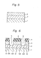
- the elements of the HEMT are the same as those of the HEMT in Fig. 2 and are denoted by. the same reference numerals.
- a surface of the second single crystalline semiconductor layer 3 is converted to an insulating layer 6 by oxidizing or nitrifying the semiconductor material of the second single crystalline semiconductor layer 3.
- the insulating layer 6 therefore consists of oxide or nitride containing the semiconductor material and is mainly composed of aluminum oxide (Al 2 O 3 ) or aluminum nitride (A1N).
- the conduction layers 7 are epitaxially grown in the grooves, part of the GaAs or the like deposited on the insulating layer 6 is grown as an amorphous layer 8 having a high resistivity while the other part of the GaAs or the like deposited on the amorphous layer 8 and the exposed first single crystalline semiconductor layer 2 is epitaxially ; grown as a single crystal and having a low resistivity.
- the conduction layers 7 consisting of a single crystalline GaAs or the like are therefore completely insulated from the second single crystalline semiconductor layer 3 by both the oxide or nitride and the amorphous layer 8 having high resistivity.
- an extremely thin insulating layer 6 of oxide or nitride formed on the second single crystalline semiconductor layer 3, which alone can otherwise cause a tunnel phenomenon or the direct conduction of current between such layer 3 and the conduction layers 7, may be used together with such an insulating amorphous layer 8 so as to achieve the complete insulation.
- the HEMT shown in this drawing has the same structure as the HEMT shown in Fig. 3 except that the position of the first and second single crystalline semiconductor layers 2 and 3, respectively, is reversed. Therefore, the electron-storing layer (not shown) is formed in the upper layer, i.e. the first single crystalline semiconductor layer 2 in proximity to the heterojunction 12. between the first and second single crystalline semiconductor layers 2 and 3, respectively.
- a heat treatment for alloying the electrode material must be precisely carried out so that the electrode material is only alloyed with respect to the first single crystalline semiconductor layer 2.
- the heat treatment leads to alloying of the electrode material with respect to not only the first single crystalline semiconductor layer 2 but also the second single crystalline layer 3.
- the insulating layer 6 insulates the conduction layers 7 from the first single crystalline semiconductor layer 2, it is easy to selectively form a current-conduction path between the source and/or drain electrodes 9A and 9B, respectively, and the second single crystalline semiconductor layer 3.
- FIG. 5 through 10 a process for producing a HEMT,-using - the present invention is illustrated.
- Undoped GaAs is epitaxially grown, by means of an MBE method, on the substrate 1, which consists of semi-insulating GaAs, so as to form a first single crystalline semiconductor layer 2 having a thickness of approximately 0.2 micron. Then the epitaxial growth of N-doped AlGaAs is carried out without interrupting molecular-beam epitaxial growth so that a second single crystalline semiconductor layer 3 is continuously grown on the first single crystalline semiconductor layer 2.
- the second single crystalline semiconductor layer 3 consists of N-doped Al 0.3 Ga 0.7 As having an impurity concentration of approximately 1x10 18 /cm 3 and has a thickness of 0.2 micron.
- a silicon dioxide layer 4 is formed on the second single crystalline semiconductor layer 3 and is subsequently selectively removed, by means of photolithography, from parts of the second single crystalline semiconductor layer 3 designated as the source and drain regions of the HEMT.
- the remaining part of the silicon dioxide layer 4 is used as a mask for the selective removal of the exposed second single crystalline semiconductor layer 3, and, as a result of such selective removal, grooves 5 are formed, preferably by means of a reactive plasma etching method, in which carbondichlo- ride difluoride (CC1 2 F 2 ) is used as the reactant.
- a monitor device such as a photodiode, which can detect the optical spectrum varying in accordance with the reactive plasma etching process, makes it possible to stop etching as stated above. Even though the first single crystalline semiconductor layer 2 is etched, the depth of etching is very small.
- the parts of the second single crystalline semiconductor layer 3 designated as the source and drain regions of the HEMT are selectively removed as described above. As a result of selective removal, the ends 12A of the hetero- junction 12 are exposed.
- the surface of the grooves 5 of the second single crystalline semiconductor layer 3 is exposed to an oxygen or nitrogen atmosphere at room temperature for a period of at least 30 minutes. This exposure may be done at an elevated temperature to promote the oxidation or nitridation. As a result of such exposure, an insulating layer 6 is formed on the surface of each groove 5.
- the insulating layer is mainly composed of aluminum oxide (A1 2 0 3 ) _ or aluminum nitride (A1N) and has a thickness of approximately 1nm (10 angstroms).
- the insulating layer 6 is very thin, it is stable enough and strong enough so that it cannot be destroyed at a temperature of 600°C at which temperature the heat treatment for epitaxial growth may be carried out.
- the first single crystalline semiconductor layer 2 exposed in the grooves 5 is exposed to an oxygen or nitrogen atmosphere, and thus insulating layer is formed on such exposed layer 2.
- an insulating layer formed on such exposed first single crystalline semiconductor layer 2 can be easily sublimated at a temperature of about 600°C during the heat treatment before the epitaxial growth, since the insulating layer is mainly composed of unstable arsenic oxide and is free of stable aluminum oxide and/or aluminum nitride.
- a silicon dioxide layer 4 (Fig. 8) is again used as a mask, and the MBE method or a vapor-phase epitaxial growth method is carried out so as to epitaxially grow highly-doped GaAs or the like.
- the highly-doped GaAs or the like deposited on and grown on the exposed first single crystalline layer 2 is single crystalline and has a low resistivity while the highly-doped G aAs or the like deposited on and grown on the insulating layer 6 is amorphous and has a high resistivity.
- the amorphous highly-doped GaAs layer is denoted by reference numeral 8.
- the single crystalline highly-doped GaAs is highly conductive, it can be used as conduction layers 7 for providing a path of current between the source and/or drain electrodes (not shown) and the conduction channel (not shown) formed in the first single crystalline semiconductor layer 2 in proximity to the heterojunction 12.
- the silicon dioxide layer 4 used as a mask is removed as shown in Fig. 9. This removal can be simply acomplished by washing the silicon dioxide layer 4 in a hydrogen-fluoride solution containing hydrogen peroxide.
- the completed HEMT is shown in Fig. 10.
- the source electrode 9A and the drain electrode 9B are formed by means of selective vacuum deposition of gold or a gold-germanium alloy.
- the gate electrode 10, which forms a Schottky barrier with respect to the second single crystalline semiconductor layer 3, is formed by means of selective vacuum deposition of aluminum, titanium, platinum, gold, or the like.
- the top surface the HEMT is provided with a surface passivation film 13 and metal leads (not shown) for wire bonding.
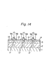
- a process for producing a HEMT is illustrated.
- the elements of the HEMT which are the same as those of the HEMTs shown in Figs. 2 through 4 and are denoted by the same reference numerals.
- the substrate 1 has lugs lA at first parts thereof designated to be positioned below the gate electrodes (not shown). These lugs lA are formed by, firstly, applying a photresist film (not shown) on the substrate 1 and, secondly, selectively removing the _photoresist film so that it remains only on said first parts and removing the exposed second parts of the substrate 1 by using the photoresist film (not shown) as a mask. To remove the exposed second parts of the substrate 1 , an ion milling method utilizing argon ions, 55nm can be used. The height of the lugs 1A may be approximately (550,angstroms). The length of the lugs lA may be approximately 2 microns. The lugs lA must have a height exceeding the thickness of the second single crystalline semiconductor layer 3 (Fig. 12) for the reasons explained hereinbelow. The photoresist film (not shown) is finally completely removed by means of a known method.
- first single crystalline semiconductor layer 2 can be formed, undoped GaAs is epitaxially grown on the first and second parts of the substrate 1 by means of the MBE method.
- the thickness of the first single crystalline semiconductor layer 2 may be approximately 0.6 micron.
- MBE growth is further continued without interruption so as to form the second single crystalline semiconductor layer 3.
- the N-doped Al 0.3 Ga 0.7 As of this layer 3 may contain silicon as the N-type conductivity impurity at a concentration of 2 x 10 18 /cm 3 and may have a thickness of approximately 30nm (300 angstroms).
- the MBE growth is further continued without interruption so as to form the conduction layers 7.
- These layers 7 consist of N -doped GaAs or Ge having an impurity concentration of 2 x 10 18 /cm 3 and has a thickness of approximately 30nm (300 angstroms).
- the substrate 1 is preferably rotated, during the MBE growth process, around an axis in the direction of the molecular beams, thereby preventing the lugs lA from shading the deposition of semiconductor materials on, for example, the second parts of the substrate 1.
- the first and second single crystalline semiconductor layers 2 and 3, respectively, have such crystal parameters that electron-storing layers 17 are formed in each lug part 2A of said second layer 2 in proximity to the hetero- junction 12.
- the conduction layers 7 are selectively left between the adjacent lug parts 3A of the second single crystalline layer 3 and are in contact with the ends 12A of heterojuction 12.
- the source electrodes 9A and the drain electrodes 9B formed on the parts of the conduction layers 7 separated from one another (Fig. 14) are electrically connected to the electron-storing layers 17 serving as the conduction channel.
- the N +- doped GaAs or Ge of the conduction layers 7 is epitaxially grown by means of the MBE method or the like, neither thermal diffusion nor ion implantation followed by annealing, is necessary in order to make a low resistance ohmic connection. So that the separated parts of the conduction layers 7 are in contact with the ends 12A of the heterojunction 12, the lug parts 1A of the substrate 1 must have a thickness greater than the thickness of the second single crystalline semiconductor layer 3.
- the single crystalline semiconductor layer in which the electron-storing layer is formed should not be intentionally doped or should be undoped.
- Undoped means that the single crystalline semiconductor is essentially free of impurities.
- Essentially free of impurities means in turn that the impurity concentration is not exactly zero but is rather of such a value that impurity scattering is effectively decreased.
- the impurity concentration of the undoped single crystalline semiconductor layer in which the electron-storing layer is formed may be approximately one tenth, at the highest, that of the other N-doped single crystalline semiconductor layer which has a less electron affinity so as to supply electrons to the electron-storing layer.
- the present invention is described hereinabove with respect to the normally on-type H E MT, the normally off-type HEMT can also be produced and has the advantages described hereinabove.
- the semiconductor elements of the HEMT have the following crystal parameters.
Landscapes
- Engineering & Computer Science (AREA)
- Microelectronics & Electronic Packaging (AREA)
- Power Engineering (AREA)
- Physics & Mathematics (AREA)
- Ceramic Engineering (AREA)
- Condensed Matter Physics & Semiconductors (AREA)
- General Physics & Mathematics (AREA)
- Computer Hardware Design (AREA)
- Junction Field-Effect Transistors (AREA)
- Bipolar Transistors (AREA)
Applications Claiming Priority (2)
| Application Number | Priority Date | Filing Date | Title |
|---|---|---|---|
| JP61702/81 | 1981-04-23 | ||
| JP56061702A JPS57176772A (en) | 1981-04-23 | 1981-04-23 | Semiconductor device and manufacture thereof |
Publications (3)
| Publication Number | Publication Date |
|---|---|
| EP0064829A2 true EP0064829A2 (de) | 1982-11-17 |
| EP0064829A3 EP0064829A3 (en) | 1985-09-25 |
| EP0064829B1 EP0064829B1 (de) | 1989-11-02 |
Family
ID=13178831
Family Applications (1)
| Application Number | Title | Priority Date | Filing Date |
|---|---|---|---|
| EP82302106A Expired EP0064829B1 (de) | 1981-04-23 | 1982-04-23 | Halbleiteranordnung mit hoher Elektronenbeweglichkeit und Verfahren zu deren Herstellung |
Country Status (4)
| Country | Link |
|---|---|
| US (1) | US4714948A (de) |
| EP (1) | EP0064829B1 (de) |
| JP (1) | JPS57176772A (de) |
| DE (1) | DE3280011D1 (de) |
Cited By (5)
| Publication number | Priority date | Publication date | Assignee | Title |
|---|---|---|---|---|
| FR2537781A1 (fr) * | 1982-12-14 | 1984-06-15 | Thomson Csf | Transistor a effet de champ, fonctionnant en regime d'accumulation par gaz d'electrons |
| EP0258530A2 (de) * | 1986-09-01 | 1988-03-09 | Licentia Patent-Verwaltungs-GmbH | Photoempfänger |
| EP0260376A1 (de) * | 1986-09-01 | 1988-03-23 | Licentia Patent-Verwaltungs-GmbH | Photoempfänger |
| EP0272384A1 (de) * | 1986-12-24 | 1988-06-29 | Licentia Patent-Verwaltungs-GmbH | Monolithisch integrierter Photoempfänger |
| GB2279806A (en) * | 1993-07-05 | 1995-01-11 | Toshiba Cambridge Res Center | Ohmic contacts for semiconductor devices |
Families Citing this family (15)
| Publication number | Priority date | Publication date | Assignee | Title |
|---|---|---|---|---|
| JPH07120807B2 (ja) * | 1986-12-20 | 1995-12-20 | 富士通株式会社 | 定電流半導体装置 |
| FR2611305B1 (fr) * | 1987-02-20 | 1990-04-27 | Labo Electronique Physique | Circuit comportant des lignes conductrices pour le transfert de signaux rapides |
| US5227644A (en) * | 1989-07-06 | 1993-07-13 | Nec Corporation | Heterojunction field effect transistor with improve carrier density and mobility |
| JPH03145139A (ja) * | 1989-10-30 | 1991-06-20 | Mitsubishi Electric Corp | 電界効果トランジスタとその製造方法 |
| US5242846A (en) * | 1989-10-30 | 1993-09-07 | Mitsubishi Denki Kabushiki Kaisha | Method of manufacturing a junction field effect transistor |
| US6444552B1 (en) * | 1999-07-15 | 2002-09-03 | Hrl Laboratories, Llc | Method of reducing the conductivity of a semiconductor and devices made thereby |
| CA2456662A1 (en) * | 2001-08-07 | 2003-02-20 | Jan Kuzmik | High electron mobility devices |
| JP2005129696A (ja) * | 2003-10-23 | 2005-05-19 | Matsushita Electric Ind Co Ltd | 半導体装置及びその製造方法 |
| US7405430B2 (en) * | 2005-06-10 | 2008-07-29 | Cree, Inc. | Highly uniform group III nitride epitaxial layers on 100 millimeter diameter silicon carbide substrates |
| DE102008021674A1 (de) * | 2008-03-31 | 2009-10-01 | Osram Opto Semiconductors Gmbh | Halbleiterbauelement und Verfahren zur Herstellung eines Halbleiterbauelements |
| KR101626463B1 (ko) * | 2010-02-26 | 2016-06-02 | 삼성전자주식회사 | 고 전자 이동도 트랜지스터의 제조방법 |
| KR102238547B1 (ko) * | 2014-10-30 | 2021-04-09 | 인텔 코포레이션 | 질화 갈륨 트랜지스터에서 2d 전자 가스에 대한 낮은 접촉 저항을 위한 소스/드레인 재성장 |
| CN108649071B (zh) * | 2018-05-17 | 2019-03-19 | 苏州汉骅半导体有限公司 | 半导体器件及其制造方法 |
| JP2021111666A (ja) * | 2020-01-08 | 2021-08-02 | ソニーセミコンダクタソリューションズ株式会社 | 化合物半導体装置及び化合物半導体装置の製造方法 |
| CN112380659A (zh) * | 2020-11-11 | 2021-02-19 | 天津大学 | 基于新型电阻模型的GaN HEMT等效电路拓扑结构 |
Citations (2)
| Publication number | Priority date | Publication date | Assignee | Title |
|---|---|---|---|---|
| EP0005059A2 (de) * | 1978-04-24 | 1979-10-31 | Western Electric Company, Incorporated | Halbleiteranordnung mit einer schichtweisen Struktur und Verfahren zu deren Herstellung |
| DE2913068A1 (de) * | 1979-04-02 | 1980-10-23 | Max Planck Gesellschaft | Heterostruktur-halbleiterkoerper und verwendung hierfuer |
Family Cites Families (4)
| Publication number | Priority date | Publication date | Assignee | Title |
|---|---|---|---|---|
| US3681668A (en) * | 1967-11-14 | 1972-08-01 | Sony Corp | Semiconductor device and a method of making the same |
| US3956033A (en) * | 1974-01-03 | 1976-05-11 | Motorola, Inc. | Method of fabricating an integrated semiconductor transistor structure with epitaxial contact to the buried sub-collector |
| US4291327A (en) * | 1978-08-28 | 1981-09-22 | Bell Telephone Laboratories, Incorporated | MOS Devices |
| DE3072175D1 (de) * | 1979-12-28 | 1990-04-26 | Fujitsu Ltd | Halbleitervorrichtungen mit heterouebergang. |
-
1981
- 1981-04-23 JP JP56061702A patent/JPS57176772A/ja active Granted
-
1982
- 1982-04-23 DE DE8282302106T patent/DE3280011D1/de not_active Expired
- 1982-04-23 EP EP82302106A patent/EP0064829B1/de not_active Expired
-
1986
- 1986-03-13 US US06/839,826 patent/US4714948A/en not_active Expired - Fee Related
Patent Citations (2)
| Publication number | Priority date | Publication date | Assignee | Title |
|---|---|---|---|---|
| EP0005059A2 (de) * | 1978-04-24 | 1979-10-31 | Western Electric Company, Incorporated | Halbleiteranordnung mit einer schichtweisen Struktur und Verfahren zu deren Herstellung |
| DE2913068A1 (de) * | 1979-04-02 | 1980-10-23 | Max Planck Gesellschaft | Heterostruktur-halbleiterkoerper und verwendung hierfuer |
Non-Patent Citations (1)
| Title |
|---|
| IEEE ELECTRON DEVICE LETTERS, vol. EDL-2, no. 1, January 1981, pages 14-15, New York, US; S.JUDAPRAWIRA et al.: "Modulation-doped MBE GaAs/n-AlchiGa1-chiAs MESFETs" * |
Cited By (7)
| Publication number | Priority date | Publication date | Assignee | Title |
|---|---|---|---|---|
| FR2537781A1 (fr) * | 1982-12-14 | 1984-06-15 | Thomson Csf | Transistor a effet de champ, fonctionnant en regime d'accumulation par gaz d'electrons |
| EP0258530A2 (de) * | 1986-09-01 | 1988-03-09 | Licentia Patent-Verwaltungs-GmbH | Photoempfänger |
| EP0260376A1 (de) * | 1986-09-01 | 1988-03-23 | Licentia Patent-Verwaltungs-GmbH | Photoempfänger |
| EP0258530A3 (de) * | 1986-09-01 | 1990-04-25 | Licentia Patent-Verwaltungs-GmbH | Photoempfänger |
| EP0272384A1 (de) * | 1986-12-24 | 1988-06-29 | Licentia Patent-Verwaltungs-GmbH | Monolithisch integrierter Photoempfänger |
| GB2279806A (en) * | 1993-07-05 | 1995-01-11 | Toshiba Cambridge Res Center | Ohmic contacts for semiconductor devices |
| GB2279806B (en) * | 1993-07-05 | 1997-05-21 | Toshiba Cambridge Res Center | Semiconductor device and method of making same |
Also Published As
| Publication number | Publication date |
|---|---|
| US4714948A (en) | 1987-12-22 |
| DE3280011D1 (en) | 1989-12-07 |
| EP0064829B1 (de) | 1989-11-02 |
| JPS57176772A (en) | 1982-10-30 |
| EP0064829A3 (en) | 1985-09-25 |
| JPS6353710B2 (de) | 1988-10-25 |
Similar Documents
| Publication | Publication Date | Title |
|---|---|---|
| EP0064829B1 (de) | Halbleiteranordnung mit hoher Elektronenbeweglichkeit und Verfahren zu deren Herstellung | |
| EP0064370B1 (de) | Halbleiteranordnung mit hoher Elektronenbeweglichkeit | |
| CA1125924A (en) | Nonalloyed ohmic contacts to n-type group iii(a)-v(a) semiconductors | |
| US4662060A (en) | Method of fabricating semiconductor device having low resistance non-alloyed contact layer | |
| KR900005560B1 (ko) | 반도체장치 및 그 제조방법 | |
| KR920003799B1 (ko) | 반도체 장치 | |
| JPH0260063B2 (de) | ||
| US6064077A (en) | Integrated circuit transistor | |
| US6057566A (en) | Semiconductor device | |
| KR20090055593A (ko) | 전계 효과 헤테로구조체 트랜지스터를 포함하는 장치 및 이의 제조 방법 | |
| US4764796A (en) | Heterojunction field effect transistor with two-dimensional electron layer | |
| US5686740A (en) | Field effect transistor with recessed gate | |
| KR100198309B1 (ko) | 쇼트키 접합을 포함하는 반도체 장치 | |
| EP0744773B1 (de) | Herstellungsverfahren für Halbleiterbauelement mit plasmabehandelter Schicht | |
| US5514606A (en) | Method of fabricating high breakdown voltage FETs | |
| US5413947A (en) | Method for manufacturing a semiconductor device with an epitaxial void | |
| JPH04233771A (ja) | 電界効果トランジスタ及びその製造方法 | |
| JPH04246836A (ja) | 電界効果トランジスタの製造方法および結晶成長用保護膜の形成方法 | |
| JP2963120B2 (ja) | 半導体装置及びその製造方法 | |
| GB2239557A (en) | High electron mobility transistors | |
| JP2728427B2 (ja) | 電界効果型トランジスタとその製法 | |
| JPH0472384B2 (de) | ||
| JP3963043B2 (ja) | 電界効果型トランジスタ用エピタキシャルウェハの製造方法 | |
| JPH06196504A (ja) | 半導体装置およびその製造方法 | |
| JPH0429225B2 (de) |
Legal Events
| Date | Code | Title | Description |
|---|---|---|---|
| PUAI | Public reference made under article 153(3) epc to a published international application that has entered the european phase |
Free format text: ORIGINAL CODE: 0009012 |
|
| AK | Designated contracting states |
Designated state(s): DE FR GB NL |
|
| PUAL | Search report despatched |
Free format text: ORIGINAL CODE: 0009013 |
|
| AK | Designated contracting states |
Designated state(s): DE FR GB NL |
|
| 17P | Request for examination filed |
Effective date: 19860320 |
|
| 17Q | First examination report despatched |
Effective date: 19871029 |
|
| GRAA | (expected) grant |
Free format text: ORIGINAL CODE: 0009210 |
|
| AK | Designated contracting states |
Kind code of ref document: B1 Designated state(s): DE FR GB NL |
|
| ET | Fr: translation filed | ||
| REF | Corresponds to: |
Ref document number: 3280011 Country of ref document: DE Date of ref document: 19891207 |
|
| PLBE | No opposition filed within time limit |
Free format text: ORIGINAL CODE: 0009261 |
|
| STAA | Information on the status of an ep patent application or granted ep patent |
Free format text: STATUS: NO OPPOSITION FILED WITHIN TIME LIMIT |
|
| 26N | No opposition filed | ||
| PGFP | Annual fee paid to national office [announced via postgrant information from national office to epo] |
Ref country code: FR Payment date: 19960410 Year of fee payment: 15 |
|
| PGFP | Annual fee paid to national office [announced via postgrant information from national office to epo] |
Ref country code: GB Payment date: 19960415 Year of fee payment: 15 |
|
| PGFP | Annual fee paid to national office [announced via postgrant information from national office to epo] |
Ref country code: DE Payment date: 19960429 Year of fee payment: 15 |
|
| PGFP | Annual fee paid to national office [announced via postgrant information from national office to epo] |
Ref country code: NL Payment date: 19960430 Year of fee payment: 15 |
|
| PG25 | Lapsed in a contracting state [announced via postgrant information from national office to epo] |
Ref country code: GB Effective date: 19970423 |
|
| PG25 | Lapsed in a contracting state [announced via postgrant information from national office to epo] |
Ref country code: NL Effective date: 19971101 |
|
| GBPC | Gb: european patent ceased through non-payment of renewal fee |
Effective date: 19970423 |
|
| PG25 | Lapsed in a contracting state [announced via postgrant information from national office to epo] |
Ref country code: FR Free format text: LAPSE BECAUSE OF NON-PAYMENT OF DUE FEES Effective date: 19971231 |
|
| PG25 | Lapsed in a contracting state [announced via postgrant information from national office to epo] |
Ref country code: DE Free format text: LAPSE BECAUSE OF NON-PAYMENT OF DUE FEES Effective date: 19980101 |
|
| NLV4 | Nl: lapsed or anulled due to non-payment of the annual fee |
Effective date: 19971101 |
|
| REG | Reference to a national code |
Ref country code: FR Ref legal event code: ST |