EP0258530A2 - Photoempfänger - Google Patents
Photoempfänger Download PDFInfo
- Publication number
- EP0258530A2 EP0258530A2 EP87105587A EP87105587A EP0258530A2 EP 0258530 A2 EP0258530 A2 EP 0258530A2 EP 87105587 A EP87105587 A EP 87105587A EP 87105587 A EP87105587 A EP 87105587A EP 0258530 A2 EP0258530 A2 EP 0258530A2
- Authority
- EP
- European Patent Office
- Prior art keywords
- semiconductor layer
- doped semiconductor
- pin diode
- monolithically integrated
- hemt
- Prior art date
- Legal status (The legal status is an assumption and is not a legal conclusion. Google has not performed a legal analysis and makes no representation as to the accuracy of the status listed.)
- Withdrawn
Links
- 239000004065 semiconductor Substances 0.000 claims abstract description 67
- 239000000758 substrate Substances 0.000 claims description 12
- 238000013461 design Methods 0.000 claims description 5
- 239000000463 material Substances 0.000 claims description 4
- 230000005669 field effect Effects 0.000 claims description 3
- 238000009413 insulation Methods 0.000 claims description 3
- 238000005516 engineering process Methods 0.000 abstract description 2
- 239000013307 optical fiber Substances 0.000 abstract description 2
- 239000002800 charge carrier Substances 0.000 description 7
- 229910001218 Gallium arsenide Inorganic materials 0.000 description 5
- 229910000530 Gallium indium arsenide Inorganic materials 0.000 description 5
- 229910001020 Au alloy Inorganic materials 0.000 description 2
- VYPSYNLAJGMNEJ-UHFFFAOYSA-N Silicium dioxide Chemical compound O=[Si]=O VYPSYNLAJGMNEJ-UHFFFAOYSA-N 0.000 description 2
- 230000000903 blocking effect Effects 0.000 description 2
- 239000013078 crystal Substances 0.000 description 2
- 238000005468 ion implantation Methods 0.000 description 2
- 238000000034 method Methods 0.000 description 2
- 230000005693 optoelectronics Effects 0.000 description 2
- 229910000927 Ge alloy Inorganic materials 0.000 description 1
- 229910000673 Indium arsenide Inorganic materials 0.000 description 1
- 239000004642 Polyimide Substances 0.000 description 1
- 229910001297 Zn alloy Inorganic materials 0.000 description 1
- 238000010521 absorption reaction Methods 0.000 description 1
- 238000000137 annealing Methods 0.000 description 1
- 230000004888 barrier function Effects 0.000 description 1
- 229910052681 coesite Inorganic materials 0.000 description 1
- 238000004891 communication Methods 0.000 description 1
- 239000004020 conductor Substances 0.000 description 1
- 229910052906 cristobalite Inorganic materials 0.000 description 1
- 230000007423 decrease Effects 0.000 description 1
- 230000007547 defect Effects 0.000 description 1
- 238000011161 development Methods 0.000 description 1
- 230000018109 developmental process Effects 0.000 description 1
- 239000002019 doping agent Substances 0.000 description 1
- 238000000407 epitaxy Methods 0.000 description 1
- 238000005530 etching Methods 0.000 description 1
- 238000011049 filling Methods 0.000 description 1
- -1 for example Inorganic materials 0.000 description 1
- RPQDHPTXJYYUPQ-UHFFFAOYSA-N indium arsenide Chemical compound [In]#[As] RPQDHPTXJYYUPQ-UHFFFAOYSA-N 0.000 description 1
- 238000002955 isolation Methods 0.000 description 1
- 238000005259 measurement Methods 0.000 description 1
- 238000001451 molecular beam epitaxy Methods 0.000 description 1
- 230000003287 optical effect Effects 0.000 description 1
- 150000002902 organometallic compounds Chemical class 0.000 description 1
- 238000002161 passivation Methods 0.000 description 1
- 229920001721 polyimide Polymers 0.000 description 1
- 239000000377 silicon dioxide Substances 0.000 description 1
- 235000012239 silicon dioxide Nutrition 0.000 description 1
- 229910052682 stishovite Inorganic materials 0.000 description 1
- 239000000126 substance Substances 0.000 description 1
- 229910052718 tin Inorganic materials 0.000 description 1
- 229910052905 tridymite Inorganic materials 0.000 description 1
- 229910052725 zinc Inorganic materials 0.000 description 1
Images

Classifications
-
- H—ELECTRICITY
- H10—SEMICONDUCTOR DEVICES; ELECTRIC SOLID-STATE DEVICES NOT OTHERWISE PROVIDED FOR
- H10F—INORGANIC SEMICONDUCTOR DEVICES SENSITIVE TO INFRARED RADIATION, LIGHT, ELECTROMAGNETIC RADIATION OF SHORTER WAVELENGTH OR CORPUSCULAR RADIATION
- H10F39/00—Integrated devices, or assemblies of multiple devices, comprising at least one element covered by group H10F30/00, e.g. radiation detectors comprising photodiode arrays
- H10F39/10—Integrated devices
- H10F39/103—Integrated devices the at least one element covered by H10F30/00 having potential barriers, e.g. integrated devices comprising photodiodes or phototransistors
Definitions
- the invention relates to a monolithically integrated photo receiver according to the preamble of patent claim 1.
- Photo receivers according to the invention are suitable for measurement or communication systems.
- Previously known solutions of monolithically integrated optoelectronic receiver circuits are, for example, a combination of a PIN diode and a JFET (junction field effect transistor) based on InGaAs (lit .: RENahory, RFLeheny, Proc.Soc.Photo-Optical Instrum. Eng. 272 (1981 ), P.32-35) or a combination of a PIN diode and a heterobipolar transistor made of InP / InGaAsp connections.
- these optoelectronic receiver circuits have the Disadvantage that they have a low switching speed and high noise figures.
- the invention is therefore based on the object of specifying a fast-switching and low-noise monolithically integrated photoreceiver which is particularly suitable for a wavelength range ⁇ of preferably 0.8 ⁇ ⁇ ⁇ 1.55 ⁇ m which is useful for optical fiber technology.
- the monolithically integrated photo receiver according to the invention has the advantage that a fast-switching field-effect transistor, whose cut-off frequency is in the GHz range, which has a high-impedance input resistance and is very low in noise, can be combined with an optical detector with high quantum efficiency and low noise.
- a heterostructure semiconductor layer sequence is made from, for example, semi-insulating substrate 5 made of InP a p-doped semiconductor layer 4 made of InP or InGaAsP with a charge carrier concentration of 1017-5.1018 cm ⁇ 3 and a layer thickness of 10-500nm, an n ⁇ -doped semiconductor layer 3 made of InGaAs with a charge carrier concentration of 1014-1016 cm ⁇ 3 and a layer thickness of 1.5-2.5 ⁇ m, an undoped semiconductor layer 2a made of InP or InGaAsP or InAlAs and a layer thickness of approximately 5 nm, an n+-doped semiconductor layer 2 made of InP or InGaAsP or InAlAs with a charge carrier concentration of 1017-2 ⁇ 1018 cm ⁇ 3 and a layer thickness of 20-100nm, - An n++-doped semiconductor layer 1 made of InGaAs or InGaAsP with a charge carrier concentration of
- the p-doped semiconductor layer 4 is preferably made of GaAs or GaAlAs, the n ⁇ -doped semiconductor layer 3 made of GaAs or In x Ga 1-x As (x ⁇ 0.1), the undoped semiconductor layer 2a made of GaAs or GaAlAs, the n+-doped semiconductor layer 2 made of GaAlAs and the n++-doped semiconductor layer 1 made of GaAs.
- the doping concentrations and layer thicknesses correspond to the exemplary embodiment described above.
- a semiconductor layer sequence can be generated, - Instead of the p-doped semiconductor layer 4, only in the area of the PIN diode 14 has a p-implanted zone 4a selective in the substrate 5 with a charge carrier concentration of 1017-1018 cm3 and a depth of approximately 0.5 ⁇ m (Fig.
- a superlattice made of lattice-matched materials such as InAlAs / InGaAs, InAlAs / InGaAsP, InP / InGaAs, InP / InGaAsP or InP / InAlAs or from materials that are lattice mismatched and whose layer thicknesses are each less than a critical layer thickness, such as, for example, GaP, GaA, InAs, InAlAs or InAlAsP.
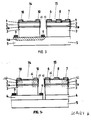
- a photo receiver is constructed from a PIN diode 14 and a HEMT (high electron mobility transistor) 15 in a mesa design.
- the source and drain connections 6, 7 of the HEMT 15 are applied to the n dot-doped semiconductor layer 1.
- the connections 6, 7 are non-blocking ohmic contacts, e.g. made of an Au / Ge alloy.
- the n++-doped semiconductor layer 1 is etched away and the control electrode 8 contacts the n+-doped semiconductor layer 2.
- the space charge zone, which is formed below the electrode 8, is controlled via a blocking metallic contact .
- the electrodes 9, 10 of the PIN diode 14 in mesa design are arranged in a ring, for example, the first electrode 10 the n++-doped semiconductor layer 1 and the second electrode 9 either the p-doped semiconductor layer 4 or the 5 implanted in the substrate Zone 4a contacted.
- the electrodes 9, 10 of the PIN diode 14 are lock-free metallic contacts and are made, for example, of an Au / Ge or Au / Zn alloy.
- n++-doped perpendicular to the semiconductor layers Regions 16 are implanted.
- the n++-doped semiconductor layer 1 can thus be omitted (FIG. 4).
- the doping concentration of the n++-implanted regions 16 is 1016-1018 charge carriers per cm3.
- the exemplary embodiment according to FIG. 2 has the same heterostructure layer sequence as the exemplary embodiment according to FIG. 1.
- the PIN diode 14 and HEMT 15 are planar.
- a semiconductor layer sequence according to FIG. 3 or FIG. 4 is also suitable for the planar design.
- the electrical connections of the HEMT 15 and the PIN diode 14 are arranged in one plane.
- the contacting of the second electrode 9a of the PIN diode 14 with the p-conducting semiconductor layer 4 or with the region 4a p-implanted into the substrate 5 takes place through a region 11 which is p-implanted perpendicular to the semiconductor layers 1 to 4 and which has a doping concentration of more than 1017 positive charge carriers per cm3.
- a first insulation region 12 which runs perpendicular to the semiconductor layers 1, 2, 2a, 3, separates the electrodes 9a, 10 of the PIN diode 14.
- a second insulation region offers 12a which runs perpendicular to the semiconductor layer sequence and extends into the substrate 5, delimits the PIN diode 14 and HEMT 15 from one another.
- the isolation regions 12, 12a are either by ion implantation, e.g. with Fe, or by suitable etching and subsequent filling techniques, e.g. with polyimide.
- a passivation and anti-reflection layer 13 is advantageously applied to the n++-doped semiconductor layer 1 or the n+-doped semiconductor layer 2. made of SiO2, in which there are windows for the electrical contacts.
- the electrical contacts of the PIN diode 14 and the HEMT 15 can be connected to one another in a suitable manner, for example via metallic conductor tracks.
- the compatibility of PIN diode 14 and HEMT 15 for producing a photoreceiver according to the invention is advantageously achieved in that the n + -doped semiconductor layer 3 is designed as an absorption layer of the PIN diode 14, has a suitable layer thickness of approximately 2 ⁇ m, so that the photons are completely absorbed, - Has a smaller band gap than the semiconductor layers 2, 2a grown on it, so that in the HEMT 14 in the n ⁇ -doped semiconductor layer 3 forms a potential well in which the electrons can move quasi-freely.
- the p-doped semiconductor layer 4 or the superlattice structure have the advantage that they act as a buffer layer between substrate 5 and the following semiconductor layers and crystal defects are essentially localized at the substrate / buffer layer interface, - no disturbing lateral conductivity occurs in the HEMT 15.
- Monolithically integrated photoreceivers according to the invention can be produced from organometallic compounds with the aid of molecular beam epitaxy or chemical gas phase epitaxy.
Landscapes
- Light Receiving Elements (AREA)
- Junction Field-Effect Transistors (AREA)
Abstract
Description
- Die Erfindung betrifft einen monolithisch integrierten Photoempfänger nach dem Oberbegriff des Patentanspruchs 1.
- Photoempfänger gemäß der Erfindung sind für Meß- oder Nachrichtenübertragungssysteme geeignet. Vorbekannte Lösungen von monolithisch integrierten optoelektronischen Empfängerschaltungen sind beispielsweise eine Kombination aus einer PIN-Diode und einem JFET(Junction Field Effect Transistor) auf InGaAs Basis(Lit.: R.E.Nahory, R.F.Leheny, Proc.Soc.Photo-Optical Instrum. Eng. 272(1981), S.32-35) oder eine Kombination aus einer PIN-Diode und einem Heterobipolartransistor aus InP/InGaAsp-Verbindungen. Diese optoelektronischen Empfängerschaltungen haben jedoch den Nachteil, daß sie eine geringe Schaltgeschwindigkeit und hohe Rauschzahlen besitzen.
- Die Erfindung liegt daher die Aufgabe zugrunde, einen schnellschaltenden und rauscharmen monolithisch integrierten Photoempfänger anzugeben, der insbesondere für einen für die Lichtleitfasertechnik nützlichen Wellenlängenbereich λ von vorzugsweise 0,8 ≦ λ ≦ 1,55µm geeignet ist.
- Diese Aufgabe wird gelöst durch die im kennzeichnenden Teil des Patentanspruchs 1 angegebenen Merkmale. Vorteilhafte Ausgestaltungen und/oder Weiterbildungen sind den Unteransprüchen entnehmbar.
- Der monolithisch integrierte Photoempfänger gemäß der Erfindung hat den Vorteil, daß ein schnellschaltender Feldeffekttransistor, dessen Grenzfrequenz im GHz-Bereich liegt, der einen hochohmigen Eingangswiderstand hat und sehr rauscharm ist, mit einem optischen Detektor mit hohem Quantenwirkungsgrad und geringem Rauschen kombiniert werden kann.
- Die Erfindung wird im folgenden anhand von Ausführungsbeispielen näher erläutert unter Bezugnahme auf schematische Zeichnungen.
- Fig. 1 Fig. 3 Fig. 4 zeigen einen monolithisch integrierten Photoempfänger bestehend aus einer PIN-Diode 14 und einem HEMT (High Electron Mobility Transistor) 15 in Mesabauweise.
- Fig. 2 zeigt einen monolithisch integrierten Photoempfänger bestehend aus einer PIN-Diode(14) und einem HEMT (15), die planar angeordnet sind.
- Im Ausführungsbeispiel gemäß Fig. 1 ist auf einem beispielsweise halbisolierenden Substrat 5 aus InP eine Heterostruktur-Halbleiterschichtenfolge aus
- einer p-dotierten Halbleiterschicht 4 aus InP oder InGaAsP mit einer Ladungsträgerkonzentration von 10¹⁷-5.10¹⁸ cm⁻³ und einer Schichtdicke von 10-500nm,
- einer n⁻⁻-dotierten Halbleiterschicht 3 aus InGaAs mit einer Ladungsträgerkonzentration von 10¹⁴-10¹⁶ cm⁻³ und einer Schichtdicke von 1,5-2,5µm,
- einer undotierten Halbleiterschicht 2a aus InP oder InGaAsP oder InAlAs und einer Schichtdicke von ungefähr 5nm,
- einer n⁺-dotierten Halbleiterschicht 2 aus InP oder InGaAsP oder InAlAs mit einer Ladungsträgerkonzentration von 10¹⁷-2 · 10¹⁸ cm⁻³ und einer Schichtdicke von 20-100nm,
- einer n⁺⁺-dotierten Halbleiterschicht 1 aus InGaAs oder InGaAsP mit einer Ladungsträgerkonzentration von 10¹⁷-6.10¹⁸ cm⁻³ und einer Schichtdicke von 0-100nm
aufgewachsen. - Besteht das Substrat 5 beispielsweise aus halbisolierendem GaAs, so ist die p-dotierte Halbleiterschicht 4 vorzugsweise aus GaAs oder GaAlAs, die n⁻⁻-dotierte Halbleiter schicht 3 aus GaAs oder InxGa1-xAs (x < 0,1), die undotierteHalbleiterschicht 2a aus GaAs oder GaAlAs, die n⁺-dotierte Halbleiterschicht 2 aus GaAlAs und die n⁺⁺-dotierte Halbleiterschicht 1 aus GaAs aufgebaut. Die Dotierkonzentrationen und Schichtdicken entsprechen dem oben beschriebenen Ausführungsbeispiel.
- Die "+"- oder "-" Bezeichnung bei der Dotierkonzentration gibt die Stärke der Dotierung an: "+" bedeutet starke und "-" schwache Dotierung.
- Alternativ zu der oben beschriebenen Heterostruktur-Halbleiterschichtenfolge kann beispielsweise eine Halbleiterschichtenfolge erzeugt werden,
- die anstatt der p-dotierten Halbleiterschicht 4 lediglich im Bereich der PIN-Diode 14 eine in das Substrat 5 selektive p-implantierte Zone 4a mit einer Ladungsträgerkonzentration von 10¹⁷-10¹⁸ cm³ und einer Tiefe von ungefähr 0,5µm besitzt (Fig. 3) und/oder
- in die anstatt der p-dotierten Halbleiterschicht 4, der n⁺-dotierten Halbleiterschicht 2 und der undotierten Halbleiterschicht 2a ein Übergitter aus gitterangepaßten materialien wie z.B. InAlAs/InGaAs, InAlAs/InGaAsP, InP/InGaAs, InP/InGaAsP bzw. InP/InAlAs oder aus gitterfehlangepaßten Materialien, deren Schichtdicken jeweils unterhalb einer kritischen Schichtdicke liegen, wie z.B. GaP, GaA, InAs, InAlAs oder InAlAsP, eingebaut ist. - Als Dotierstoffe für p-Dotierung werden beispielsweise Be, Mg oder Zn und für n-Dotierung Si, S oder Sn verwendet. Die durch Ionenimplantation entstandenen Schäden im Kristall werden durch einen anschließenden Temperprozeß ausgeheilt.
- In den Ausführungsbeispielen gemäß Fig. 1 und Fig. 3 ist ein Photoempfänger aus einer PIN-Diode 14 und einem HEMT (High Electron Mobility Transistor) 15 in Mesabauweise aufgebaut. Source- und Drain-Anschluß 6, 7 des HEMT 15 sind auf der n⁺⁺-dotierten Halbleiterschicht 1 aufgebracht. Die Anschlüsse 6, 7 sind sperrfreie ohmsche Kontakte, z.B. aus einer Au/Ge-Legierung. Im Bereich der Steuelektrode 8 des HEMT 15 ist die n⁺⁺-dotierte Halbleiterschicht 1 weggeätzt und die Steuerelektrode 8 kontaktiert die n⁺-dotierte Halbleiterschicht 2. Die Steuerung der Raumladungszone, die sich unterhalb der Elektrode 8 ausbildet, erfolgt über einen sperrenden metallischen Kontakt. Zur Verbesserung der Sperreigenschaften der Steuerelektrode 8 ist es vorteilhaft, die n⁺-Dotierung der Halbleiterschicht 2 in vertikaler Richtung zu variieren, derart, daß die Dotierkonzentration zur n⁺⁺-dotierten Halbleiterschicht 1 auf Null abnimmt.
- Die Elektroden 9, 10 der PIN-Diode 14 in Mesabauweise sind beispielsweise ringförmig angeordnet, wobei die erste Elektrode 10 die n⁺⁺-dotierte Halbleiterschicht 1 und die zweite Elektrode 9 entweder die p-dotierte Halbleiterschicht 4 oder die in das Substrat 5-implantierte Zone 4a kontaktiert. Die Elektroden 9, 10 der PIN-Diode 14 sind sperrfreie metallische Kontakte und sind beispielsweise aus einer Au/Ge- oder Au/Zn-Legierung hergestellt.
- Zur Verbesserung der Kontaktierung der n⁻⁻-dotierten Halbleiterschicht 3 der PIN-Diode 14 bzw. des sich zwischen der undotierten Halbleiterschicht 2a und der n⁻⁻-dotierten Halbleiterschicht 3 im HEMT 15 ausbildenden Elektronengases können senkrecht zu den Halbleiterschichten n⁺⁺-dotierte Gebiete 16 implantiert werden. Die n⁺⁺-dotierte Halbleiterschicht 1 kann dadurch entfallen (Fig. 4). Die Dotierkonzentration der n⁺⁺-implantierten Gebiete 16 beträgt 10¹⁶-10¹⁸ Ladungsträger pro cm³.
- Das Ausführungsbeispiel gemäß Fig. 2 besitzt die gleiche Heterostruktur-Schichtenfolge wie das Ausführungsbeispiel gemäß Fig. 1. Jedoch sind PIN-Diode 14 und HEMT 15 planar ausgebildet. Für die planare Bauform ist auch eine Halbleiterschichtenfolge gemäß Fig.3 oder Fig. 4 geeignet. Die elektrischen Anschlüsse des HEMT 15 und der PIN-Diode 14 sind in einer Ebene angeordnet. Die Kontaktierung der zweiten Elektrode 9a der PIN-Diode 14 mit der p-leitenden Halbleiterschicht 4 bzw. mit der in das Substrat 5 p-implantierten Zone 4a erfolgt durch ein senkrecht zu den Halbleiterschichten 1 bis 4 p-implantiertes Gebiet 11, das eine Dotierkonzentration von mehr als 10¹⁷ positiven Ladungsträgern pro cm³ besitzt.
- Ein erstes Isolationsgebiet 12, das senkrecht zu den Halbleiterschichten 1, 2, 2a, 3 verläuft, trennt die Elektroden 9a, 10 der PIN-Diode 14. Ein zweites Isolationsge biet 12a, das senkrecht zu der Halbleiterschichtenfolge verläuft und bis ins Substrat 5 reicht, grenzt PIN-Diode 14 und HEMT 15 voneinander ab.
- Die Isolationsgebiete 12, 12a werden entweder durch Ionenimplantation, z.B. mit Fe, oder durch geeignete Ätz- und anschließende Auffülltechniken, z.B. mit Polyimid, hergestellt.
- In den Ausführungsbeispielen ist vorteilhafterweise auf die n⁺⁺-dotierte Halbleiterschicht 1 oder die n⁺-dotierte Halbleiterschicht 2 eine Passivierungs- und Antireflexionsschicht 13, z.B. aus SiO₂, aufgetragen, in der sich Fenster für die elektrischen Kontakte befinden.
- Die elektrischen Kontakte der PIN-Diode 14 und des HEMT 15 können beispielsweise über metallische Leiterbahnen in geeigneter Weise miteinander verbunden werden.
- Vorteilhafterweise wird die Kompatibilität von PIN-Diode 14 und HEMT 15 zur Herstellung eines erfindungsgemäßen Photoempfängers dadurch erreicht, daß die n⁻⁻-dotierte Halbleiterschicht 3
- als Absorptionsschicht der PIN-Diode 14 ausgebildet ist,
- eine geeignete Schichtdicke von ungefähr 2µm besitzt, so daß die Photonen vollständig absorbiert werden,
- einen geringeren Bandabstand als die darauf aufgewachsenen Halbleiterschichten 2, 2a besitzt, damit sich im HEMT 14 in der n⁻⁻-dotierten Halbleiter schicht 3 ein Potentialtopf ausbildet, in dem sich die Elektronen quasi-frei bewegen können. - Die p-dotierte Halbleiterschicht 4 oder die Übergitterstruktur haben den Vorteil, daß
- sie als Pufferschicht zwischen Substrat 5 und den folgenden Halbleiterschichten wirken und Kristalldefekte im wesentlichen an der Grenzfläche Substrat/Pufferschicht lokalisiert sind,
- im HEMT 15 keine störende laterale Leitfähigkeit auftritt. - Monolithisch integrierte Photoempfänger gemäß der Erfindung, lassen sich mit Hilfe der Molekularstrahl-Epitaxie oder der chemischen Gasphasen-Epitaxie aus metallorganischen Verbindungen herstellen.
- Die Erfindung ist nicht auf die beschriebenen Ausführungsbeispiele beschränkt, sondern sinngemäß auf weitere Materialkombinationen anwendbar.
Claims (11)
- daß PIN-Diode (14) und HEMT (15) aus einer gleichen Heterostruktur-Halbleiterschichtenfolge hergestellt sind,
- daß auf einem Substrat (5) mindestens eine p-dotierte Halbleiterschicht (4) aufgewachsen ist, und
- daß die p-dotierte Halbleiterscicht (4) gleichzeitig als invertiert angeordnete p-Kontaktschicht der PIN-Diode (14) und als Pufferschicht ausgebildet ist.
- daß die Steuerelektrode (8) des HEMT (15) mit der n⁺-dotierten Halbleiterschicht (2) kontaktiert ist und
- daß Source- und Drain-Anschluß (6, 7) des HEMT (15) auf der n⁺⁺-dotierten Halbleiterschicht (1) aufgebracht sind.
- daß die n⁺⁺-dotierte Halbleiterschicht (1) entfernt ist, und
- daß die n-Kontaktierung der elektrischen Anschlüsse (6, 7, 10) der PIN-Diode (14) und des HEMT (15) über n⁺⁺-implantierte Gebiete (16) erfolgt, die senkrecht zu den Halbleiterschichten (2, 2a) verlaufen und bis in die n⁻⁻-dotierte Halbleiterschicht (3) reichen (Fig. 4).
- daß die zweite Elektrode (9a) der PIN-Diode (14) durch ein p-implantiertes Gebiet (11) die p-dotierte Halbleiterschicht (4) kontaktiert, und
- daß die Elektroden (9a, 10) der PIN-Diode (14) durch ein erstes Isolationsgebiet (12) abgegrenzt sind, das senkrecht zu den Halbleiterschichten (1, 2, 2a) verläuft und bis in die n⁻⁻-dotierte Halbleiterschicht (3) reicht.
Applications Claiming Priority (2)
| Application Number | Priority Date | Filing Date | Title |
|---|---|---|---|
| DE3629681 | 1986-09-01 | ||
| DE19863629681 DE3629681A1 (de) | 1986-09-01 | 1986-09-01 | Photoempfaenger |
Publications (2)
| Publication Number | Publication Date |
|---|---|
| EP0258530A2 true EP0258530A2 (de) | 1988-03-09 |
| EP0258530A3 EP0258530A3 (de) | 1990-04-25 |
Family
ID=6308646
Family Applications (1)
| Application Number | Title | Priority Date | Filing Date |
|---|---|---|---|
| EP87105587A Withdrawn EP0258530A3 (de) | 1986-09-01 | 1987-04-15 | Photoempfänger |
Country Status (2)
| Country | Link |
|---|---|
| EP (1) | EP0258530A3 (de) |
| DE (1) | DE3629681A1 (de) |
Cited By (6)
| Publication number | Priority date | Publication date | Assignee | Title |
|---|---|---|---|---|
| EP0417348A1 (de) * | 1989-09-15 | 1991-03-20 | Siemens Aktiengesellschaft | Verfahren zur Herstellung eines dotierten Bereiches in einer Halbleiterschicht |
| US5032885A (en) * | 1988-12-17 | 1991-07-16 | Sumitomo Electric Industries, Ltd. | Semiconductor device including a light receiving element, an amplifier, and an equalizer having a capacitor with the same laminate structure as the light receiving element |
| US5035479A (en) * | 1988-06-17 | 1991-07-30 | Interuniversitair Micro-Elektronica Centrum Vzw | Device for optical signal processing showing transistor operation |
| CN100552991C (zh) * | 2006-09-27 | 2009-10-21 | 中国科学院半导体研究所 | 声子调控间接带隙半导体材料横向电注入发光器件 |
| CN106783744A (zh) * | 2016-12-27 | 2017-05-31 | 成都海威华芯科技有限公司 | 一种InP PIN光电探测器集成器件的制作方法 |
| CN109216331A (zh) * | 2018-07-23 | 2019-01-15 | 西安电子科技大学 | 一种基于pin二极管的毫米波预失真集成电路及制作方法 |
Families Citing this family (4)
| Publication number | Priority date | Publication date | Assignee | Title |
|---|---|---|---|---|
| DE3908886A1 (de) * | 1989-03-17 | 1990-09-20 | Siemens Ag | Doppel-pin-photodiode mit sperrendem p-n-uebergang zwischen substrat und absorptionsschicht |
| DE19533204A1 (de) * | 1995-09-08 | 1997-03-13 | Daimler Benz Ag | Monolithisch integrierte Anordnung von PIN-Diode und Feldeffekttransistor und Verfahren zu deren Herstellung |
| DE19533205A1 (de) * | 1995-09-08 | 1997-03-13 | Daimler Benz Ag | Monolithische integrierte Anordnung von PIN-Diode und Feldeffekttransistor und Verfahren zu deren Herstellung |
| KR100670828B1 (ko) * | 2005-12-12 | 2007-01-19 | 한국전자통신연구원 | 적외선 레이저 레이다의 영상 신호를 검출하기 위한 광검출기 및 그 제조방법 |
Family Cites Families (7)
| Publication number | Priority date | Publication date | Assignee | Title |
|---|---|---|---|---|
| JPS57176772A (en) * | 1981-04-23 | 1982-10-30 | Fujitsu Ltd | Semiconductor device and manufacture thereof |
| EP0067566A3 (de) * | 1981-06-13 | 1985-08-07 | Plessey Overseas Limited | Integrierter Lichtdetektor oder -generator mit Verstärker |
| JPS58147165A (ja) * | 1982-02-26 | 1983-09-01 | Fujitsu Ltd | 半導体装置 |
| JPS5963769A (ja) * | 1982-10-05 | 1984-04-11 | Agency Of Ind Science & Technol | 高速半導体素子 |
| GB2145279B (en) * | 1983-08-18 | 1987-10-21 | Standard Telephones Cables Ltd | Photodetector integrated circuit |
| GB2168528B (en) * | 1984-12-15 | 1988-07-13 | Stc Plc | Photo detector integrated circuit |
| JPS61187363A (ja) * | 1985-02-15 | 1986-08-21 | Fujitsu Ltd | 光集積回路装置 |
-
1986
- 1986-09-01 DE DE19863629681 patent/DE3629681A1/de not_active Ceased
-
1987
- 1987-04-15 EP EP87105587A patent/EP0258530A3/de not_active Withdrawn
Cited By (7)
| Publication number | Priority date | Publication date | Assignee | Title |
|---|---|---|---|---|
| US5035479A (en) * | 1988-06-17 | 1991-07-30 | Interuniversitair Micro-Elektronica Centrum Vzw | Device for optical signal processing showing transistor operation |
| US5032885A (en) * | 1988-12-17 | 1991-07-16 | Sumitomo Electric Industries, Ltd. | Semiconductor device including a light receiving element, an amplifier, and an equalizer having a capacitor with the same laminate structure as the light receiving element |
| EP0417348A1 (de) * | 1989-09-15 | 1991-03-20 | Siemens Aktiengesellschaft | Verfahren zur Herstellung eines dotierten Bereiches in einer Halbleiterschicht |
| CN100552991C (zh) * | 2006-09-27 | 2009-10-21 | 中国科学院半导体研究所 | 声子调控间接带隙半导体材料横向电注入发光器件 |
| CN106783744A (zh) * | 2016-12-27 | 2017-05-31 | 成都海威华芯科技有限公司 | 一种InP PIN光电探测器集成器件的制作方法 |
| CN109216331A (zh) * | 2018-07-23 | 2019-01-15 | 西安电子科技大学 | 一种基于pin二极管的毫米波预失真集成电路及制作方法 |
| CN109216331B (zh) * | 2018-07-23 | 2020-07-17 | 西安电子科技大学 | 一种基于pin二极管的毫米波预失真集成电路及制作方法 |
Also Published As
| Publication number | Publication date |
|---|---|
| EP0258530A3 (de) | 1990-04-25 |
| DE3629681A1 (de) | 1988-03-10 |
Similar Documents
| Publication | Publication Date | Title |
|---|---|---|
| DE3786363T2 (de) | Halbleiteranordnungen mit hoher Beweglichkeit. | |
| DE69835204T2 (de) | ENTWURF UND HERSTELLUNG VON ELEKTRONISCHEN ANORDNUNGEN MIT InAlAsSb/AlSb BARRIERE | |
| DE69127574T2 (de) | Lawinenphotodiode mit Schutzring und Verfahren zu deren Herstellung | |
| DE69124766T2 (de) | Elektronenwelleninterferenz-Bauelement und diesbezügliches Verfahren zur Modulation eines Interferenzstromes | |
| DE19640003B4 (de) | Halbleitervorrichtung und Verfahren zu dessen Herstellung | |
| DE69226220T2 (de) | Transistor mit hoher Elektronenbeweglichkeit und Verfahren zu seiner Herstellung | |
| EP0405214A2 (de) | Pin-FET-Kombination mit vergrabener p-Schicht | |
| EP0258530A2 (de) | Photoempfänger | |
| EP0307850B1 (de) | Si/SiGe-Halbleiterkörper | |
| DE3751892T2 (de) | Halbleiteranordnung mit zwei Verbindungshalbleitern und Verfahren zu ihrer Herstellung | |
| EP0400399A2 (de) | Monolithisch integrierte Photodiode-FET-Kombination | |
| DE3712864C2 (de) | Monolithisch integrierter Photoempfänger | |
| DE3686047T2 (de) | Monolithische halbleiterstruktur bestehend aus einem laser und einem feldeffekttransistor und deren herstellungsverfahren. | |
| DE69019200T2 (de) | Verfahren zur Herstellung einer Halbleitervorrichtung mit einer Mesa-Struktur. | |
| EP0205164B1 (de) | Struktur einer Halbleiteranordnung | |
| EP0272384B1 (de) | Monolithisch integrierter Photoempfänger | |
| DE69327012T2 (de) | Bauelement mit einer räumlichen Transfer verwendenden Halbleiteranordnung | |
| DE3629685C2 (de) | Photoempfänger | |
| EP0272372B1 (de) | Verfahren zur Herstellung eines monolithisch integrierten Photoempfängers | |
| DE3709302C2 (de) | Monolithisch integrierte Senderanordnung sowie Verfahren zu ihrer Herstellung | |
| DE3781285T2 (de) | Bipolarer heterouebergangstransistor mit einem basisbereich aus germanium. | |
| DE3874949T2 (de) | Heterouebergang-bipolartransistor. | |
| DE3629684A1 (de) | Photoempfaenger | |
| DE19746920B4 (de) | Halbleitervorrichtung mit einer InGaP-Kanalschicht und einer Pufferschicht, sowie Verfahren zum Herstellen derselben | |
| WO1993013560A1 (de) | Elektronisches bauelement und verfahren zu dessen herstellung |
Legal Events
| Date | Code | Title | Description |
|---|---|---|---|
| PUAI | Public reference made under article 153(3) epc to a published international application that has entered the european phase |
Free format text: ORIGINAL CODE: 0009012 |
|
| AK | Designated contracting states |
Kind code of ref document: A2 Designated state(s): DE FR GB IT |
|
| PUAL | Search report despatched |
Free format text: ORIGINAL CODE: 0009013 |
|
| AK | Designated contracting states |
Kind code of ref document: A3 Designated state(s): DE FR GB IT |
|
| STAA | Information on the status of an ep patent application or granted ep patent |
Free format text: STATUS: THE APPLICATION IS DEEMED TO BE WITHDRAWN |
|
| 18D | Application deemed to be withdrawn |
Effective date: 19901026 |
|
| RIN1 | Information on inventor provided before grant (corrected) |
Inventor name: KOENIG, ULF, DR.-ING. Inventor name: DAEMBKES, HEINRICH, DR.-ING. |