EP0058102B1 - Verfahren zur Herstellung eines kapazitiven Feuchtigkeitsfühlers mit dünnem Dielektrikum - Google Patents
Verfahren zur Herstellung eines kapazitiven Feuchtigkeitsfühlers mit dünnem Dielektrikum Download PDFInfo
- Publication number
- EP0058102B1 EP0058102B1 EP82400072A EP82400072A EP0058102B1 EP 0058102 B1 EP0058102 B1 EP 0058102B1 EP 82400072 A EP82400072 A EP 82400072A EP 82400072 A EP82400072 A EP 82400072A EP 0058102 B1 EP0058102 B1 EP 0058102B1
- Authority
- EP
- European Patent Office
- Prior art keywords
- electrode
- layer
- process according
- dielectric material
- deposited
- Prior art date
- Legal status (The legal status is an assumption and is not a legal conclusion. Google has not performed a legal analysis and makes no representation as to the accuracy of the status listed.)
- Expired
Links
- 238000004519 manufacturing process Methods 0.000 title claims description 7
- 238000000034 method Methods 0.000 claims description 34
- 230000008569 process Effects 0.000 claims description 23
- XLYOFNOQVPJJNP-UHFFFAOYSA-N water Substances O XLYOFNOQVPJJNP-UHFFFAOYSA-N 0.000 claims description 23
- 229920000642 polymer Polymers 0.000 claims description 22
- 229910052751 metal Inorganic materials 0.000 claims description 19
- 239000002184 metal Substances 0.000 claims description 19
- 239000003989 dielectric material Substances 0.000 claims description 15
- PXHVJJICTQNCMI-UHFFFAOYSA-N Nickel Chemical compound [Ni] PXHVJJICTQNCMI-UHFFFAOYSA-N 0.000 claims description 8
- PCHJSUWPFVWCPO-UHFFFAOYSA-N gold Chemical compound [Au] PCHJSUWPFVWCPO-UHFFFAOYSA-N 0.000 claims description 8
- 229910052737 gold Inorganic materials 0.000 claims description 8
- 239000010931 gold Substances 0.000 claims description 8
- 229920002678 cellulose Polymers 0.000 claims description 5
- 239000000126 substance Substances 0.000 claims description 5
- XUIMIQQOPSSXEZ-UHFFFAOYSA-N Silicon Chemical compound [Si] XUIMIQQOPSSXEZ-UHFFFAOYSA-N 0.000 claims description 4
- 239000001913 cellulose Substances 0.000 claims description 4
- 229910052759 nickel Inorganic materials 0.000 claims description 4
- 230000003647 oxidation Effects 0.000 claims description 4
- 238000007254 oxidation reaction Methods 0.000 claims description 4
- 229910052710 silicon Inorganic materials 0.000 claims description 4
- 239000010703 silicon Substances 0.000 claims description 4
- VYZAMTAEIAYCRO-UHFFFAOYSA-N Chromium Chemical compound [Cr] VYZAMTAEIAYCRO-UHFFFAOYSA-N 0.000 claims description 3
- 229910052804 chromium Inorganic materials 0.000 claims description 3
- 239000011651 chromium Substances 0.000 claims description 3
- 238000000151 deposition Methods 0.000 claims description 3
- 150000002739 metals Chemical class 0.000 claims description 3
- 238000005520 cutting process Methods 0.000 claims description 2
- 238000005530 etching Methods 0.000 claims description 2
- 238000010438 heat treatment Methods 0.000 claims description 2
- 230000005855 radiation Effects 0.000 claims description 2
- 230000004927 fusion Effects 0.000 claims 4
- 239000004020 conductor Substances 0.000 claims 1
- 239000010410 layer Substances 0.000 description 41
- 230000008018 melting Effects 0.000 description 8
- 238000002844 melting Methods 0.000 description 8
- 239000000463 material Substances 0.000 description 6
- 239000000758 substrate Substances 0.000 description 6
- 239000003990 capacitor Substances 0.000 description 5
- 239000011521 glass Substances 0.000 description 4
- 239000011810 insulating material Substances 0.000 description 4
- 230000004044 response Effects 0.000 description 4
- 229910052782 aluminium Inorganic materials 0.000 description 3
- XAGFODPZIPBFFR-UHFFFAOYSA-N aluminium Chemical compound [Al] XAGFODPZIPBFFR-UHFFFAOYSA-N 0.000 description 3
- 230000008901 benefit Effects 0.000 description 3
- 230000007547 defect Effects 0.000 description 3
- VYPSYNLAJGMNEJ-UHFFFAOYSA-N Silicium dioxide Chemical compound O=[Si]=O VYPSYNLAJGMNEJ-UHFFFAOYSA-N 0.000 description 2
- 229920006217 cellulose acetate butyrate Polymers 0.000 description 2
- 230000000694 effects Effects 0.000 description 2
- 230000035945 sensitivity Effects 0.000 description 2
- 229910052814 silicon oxide Inorganic materials 0.000 description 2
- 238000005476 soldering Methods 0.000 description 2
- 239000002904 solvent Substances 0.000 description 2
- GUTLYIVDDKVIGB-OUBTZVSYSA-N Cobalt-60 Chemical compound [60Co] GUTLYIVDDKVIGB-OUBTZVSYSA-N 0.000 description 1
- PQLZZALLLYUAKL-UHFFFAOYSA-N [Au].[Cr].[Ni] Chemical compound [Au].[Cr].[Ni] PQLZZALLLYUAKL-UHFFFAOYSA-N 0.000 description 1
- 231100000987 absorbed dose Toxicity 0.000 description 1
- 239000002253 acid Substances 0.000 description 1
- 150000007513 acids Chemical class 0.000 description 1
- PNEYBMLMFCGWSK-UHFFFAOYSA-N aluminium oxide Inorganic materials [O-2].[O-2].[O-2].[Al+3].[Al+3] PNEYBMLMFCGWSK-UHFFFAOYSA-N 0.000 description 1
- 239000012298 atmosphere Substances 0.000 description 1
- CJZGTCYPCWQAJB-UHFFFAOYSA-L calcium stearate Chemical compound [Ca+2].CCCCCCCCCCCCCCCCCC([O-])=O.CCCCCCCCCCCCCCCCCC([O-])=O CJZGTCYPCWQAJB-UHFFFAOYSA-L 0.000 description 1
- 235000013539 calcium stearate Nutrition 0.000 description 1
- 239000008116 calcium stearate Substances 0.000 description 1
- 230000008859 change Effects 0.000 description 1
- 239000013043 chemical agent Substances 0.000 description 1
- 239000003795 chemical substances by application Substances 0.000 description 1
- 230000007797 corrosion Effects 0.000 description 1
- 238000005260 corrosion Methods 0.000 description 1
- 230000008021 deposition Effects 0.000 description 1
- 238000001035 drying Methods 0.000 description 1
- 238000005516 engineering process Methods 0.000 description 1
- 230000005251 gamma ray Effects 0.000 description 1
- 238000010849 ion bombardment Methods 0.000 description 1
- 238000005259 measurement Methods 0.000 description 1
- 239000000155 melt Substances 0.000 description 1
- 238000001465 metallisation Methods 0.000 description 1
- 230000004048 modification Effects 0.000 description 1
- 238000012986 modification Methods 0.000 description 1
- 230000003287 optical effect Effects 0.000 description 1
- TWNQGVIAIRXVLR-UHFFFAOYSA-N oxo(oxoalumanyloxy)alumane Chemical compound O=[Al]O[Al]=O TWNQGVIAIRXVLR-UHFFFAOYSA-N 0.000 description 1
- 229920006254 polymer film Polymers 0.000 description 1
- 229920002689 polyvinyl acetate Polymers 0.000 description 1
- 239000011118 polyvinyl acetate Substances 0.000 description 1
- 239000011241 protective layer Substances 0.000 description 1
- 239000007787 solid Substances 0.000 description 1
- 239000010409 thin film Substances 0.000 description 1
- 238000007738 vacuum evaporation Methods 0.000 description 1
Images

Classifications
-
- G—PHYSICS
- G01—MEASURING; TESTING
- G01N—INVESTIGATING OR ANALYSING MATERIALS BY DETERMINING THEIR CHEMICAL OR PHYSICAL PROPERTIES
- G01N27/00—Investigating or analysing materials by the use of electric, electrochemical, or magnetic means
- G01N27/02—Investigating or analysing materials by the use of electric, electrochemical, or magnetic means by investigating impedance
- G01N27/22—Investigating or analysing materials by the use of electric, electrochemical, or magnetic means by investigating impedance by investigating capacitance
- G01N27/223—Investigating or analysing materials by the use of electric, electrochemical, or magnetic means by investigating impedance by investigating capacitance for determining moisture content, e.g. humidity
- G01N27/225—Investigating or analysing materials by the use of electric, electrochemical, or magnetic means by investigating impedance by investigating capacitance for determining moisture content, e.g. humidity by using hygroscopic materials
Definitions
- the present invention relates to a process for producing a capacitive hygrometer with a thin dielectric.
- the first category is characterized by the fact that the dielectric material consists of a polymer sheet which serves both as a sensitive element and as a mechanical support for the sensor. This leads to a certain number of drawbacks for this type of hygrometer: low mechanical resistance, deformation of the polymer resulting in a notable hysteresis effect and a certain temperature coefficient.
- the sensors of the second category are formed by a layer of polymer (Vaisala) or other molecules sensitive to water (Barraud and AI) deposited on a solid metallized substrate forming the first electrode of a capacitor.
- the mechanical support of the hygrometer generally glass or another material inert to humidity, is very distinct from the water-sensitive layer.
- Document DE-B-2 938 434 describes a capacitive hygrometer in which the dielectric is made sensitive to water by ion bombardment.
- the two electrodes face each other and are separated by the dielectric, one being on a support and the other exposed to moisture.
- the exposed electrode is very thin and this hygrometer has the above mentioned defects.
- the subject of the present invention is precisely a process for producing a capacitive hygrometer which eliminates these drawbacks by making it possible to use as a water-permeable electrode a metal layer sufficiently thick to have good mechanical resistance.
- the softening temperature of the dielectric is generally close to its melting temperature.
- This treatment causes a modification of the structure of the material constituting the dielectric, which leads to a permanent deformation of the second electrode: the latter takes on a grainy structure with grains whose dimensions are of the order of a micron.
- a good porosity of the metal layer is thus obtained which becomes permeable to water vapor while retaining good mechanical strength, and in particular good mechanical strength with regard to sudden temperature variations.
- a metal substrate 2 which constitutes the first electrode 3 of a capacitive hygrometer.
- this electrode 3 is made of aluminum and rests on a rigid support 5, for example a glass plate, but a relatively thick conductive layer can be used, for example a neck.
- che silicon which itself constitutes a rigid support.
- one of the faces 4 of the first electrode is oxidized to a depth of approximately 50 to 200 A and this face is in contact with a layer 6 of an insulating material which constitutes the dielectric of the capacitor and of which the dielectric constant varies depending on the amount of water absorbed.
- a polymer naturally sensitive to water such as cellulose esters, cellulose acetate butyrate or polyvinyl acetate. It is also possible to use polymers which can take on a crosslinked structure under the effect of temperature or of ultraviolet radiation, such as cellulose acetocrotonate or cellulose aceto-butyro-crotonate. This gives hygrometers which are particularly resistant to heat and chemical agents (acids, solvents, polluting agents, etc.).
- a metallic layer 8 which constitutes the second electrode 9.
- This is preferably constituted by a slightly oxidizable metal such as gold, deposited in a relatively thick layer (more than 200 A) and rendered permeable to water by further treatment.
- the hygrometer may optionally include one or more monomolecular layers of an organic substance which protects the permeable electrode against corrosion, but the presence of these monomolecular layers is not essential.
- FIG. 2 illustrates an embodiment of the method which is the subject of the invention.
- an aluminum layer 2 which constitutes the first electrode 3 is deposited, for example by vacuum evaporation.
- an insulating block is deposited at 11, next to the layer 2. silicon oxide.
- one of the angles of the electrode 3 has been cut so that the insulating block 11 can be placed in the notch and in contact with the electrode 3.
- the block 11 has a thickness substantially equal to that of the electrode 3 so that the dielectric material 6 can be deposited on the flat surface formed by the electrode 2 and the block 11. The role of the latter will be explained below during this description.
- the aluminum layer is subjected to an anodic oxidation treatment in order to form the thin layer of alumina 4.
- the next step consists in depositing the layer of water-sensitive insulating material 6.
- a polymer cellulose acetate butyrate for example
- the dielectric is constituted by organic monomolecular layers, these are deposited by the method known as “of Langmuir and Blodgett”, and the thickness of the contained layer is of the order of approximately 500 A.
- An organic substance such as calcium stearate is very suitable for this use.
- the dielectric thus obtained is not naturally permeable to water and it must be permeabilized by a special treatment which may be a gamma-ray or electron irradiation treatment.
- gamma rays from a Cobalt 60 source are used.
- the absorbed dose is of the order of 40 Mrads, and in any case greater than 20 Mrads, this dose being absorbed for a greater duration 1 hour.
- the next step consists in producing the second electrode 9 which can be a layer of gold with a thickness greater than 200 ⁇ , deposited by any known means and in particular by vacuum metallization. Because of its thickness, this layer of gold is not permeable to water. According to a characteristic of the invention, it is made permeable by subjecting the sensor to a heat treatment at a temperature close to the softening temperature of the dielectric. Most of the materials used to form the dielectric layer have softening temperatures between 150 and 250 ° C, that is to say close to their melting temperature. It suffices to subject the hygrometer for a few minutes to this temperature in a normal atmosphere, the capacitor being de-energized, to obtain a change in the structure of the dielectric which causes permanent deformation of the gold layer.
- the protective layer of the second electrode is then produced which is in the form of one or more monomolecular layers of an organic substance deposited by the method of Langmuir and Blodgett.
- the dielectric layer 6 does not completely cover the electrode 3, which allows the first contact 12 to be soldered directly the exposed part of the electrode 3 by piercing the surface oxide layer 4.
- the permeable electrode 9 it extends over the layer 6 both above the first electrode 3 and above the insulating block 11. It is on the part of the electrode 9 located above the block 11 that the second electrical contact 13 is welded.
- the contacts can be soldered through the polymer.
- the dielectric layer 6 can completely cover the first electrode 3 since the polymer melts when the first contact 12 is welded and the second contact 13 can be welded astride the second electrode 9 and the insulating block 11. If a polymer with a high melting point (melting temperature above 300 ° C.) is used, the second contact 13 is welded to the electrode 9, as illustrated in FIG. 2, but the polymer must be removed, for example by etching , before soldering the first contact 12.
- the first contact is made directly on the solderless conductive substrate.
- the polymer is at a high melting point, it is possible to remove the insulating block 11 and weld the second contact on the upper electrode 9. If the polymer is at low melting point, the second contact is welded saddle on the permeable electrode and an insulating block.
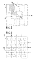
- FIG. 3 shows an arrangement allowing several hygrometers to be produced from an element 15 which is cut out according to the arrows.
- the first electrode is deposited as if the element 15 constituted a single sensor, but the insulating block 11 is placed in the center of the element 15 so as to extend over each of the sensors which will be obtained after cutting (four in the example described here).
- the second electrode 9 it has a part 9a extending over most of the block 11 and parts 9b corresponding to each of the hygrometers.
- FIG. 4 illustrates a method making it possible to manufacture a large number of sensors from a support 16 in which several elements such as the element 15 described with reference to FIG. 3 are produced.
- the method according to the invention has many advantages.
- the fact that the second electrode consists of a thick metallic layer made permeable to water by an appropriate treatment eliminates all the disadvantages of thin electrodes by facilitating the manufacturing process and by making the electrode less sensitive to pollution, which increases the lifespan of the sensor.
- the presence on the first electrode of an oxide layer which constitutes a second dielectric in series with the water-sensitive insulating material avoids short circuits between the electrodes, makes it possible to use a very thick low of this water-sensitive material and gives the assembly a large specific capacity, which allows a good connection with the means for measuring the dielectric constant.
- the permeable electrode can be made of gold or of another metal which is not very oxidizable such as chromium or nickel. It is also possible to use several layers of different metals chosen from the aforementioned metals, for example a nickel layer covered with gold or a triple chromium-nickel-gold layer.
- the sensors obtained by the method according to the invention can be used to measure any quantity the variation of which results in a variation of the dielectric constant of the material insulating.
Landscapes
- Chemical & Material Sciences (AREA)
- Chemical Kinetics & Catalysis (AREA)
- Electrochemistry (AREA)
- Physics & Mathematics (AREA)
- Health & Medical Sciences (AREA)
- Life Sciences & Earth Sciences (AREA)
- Analytical Chemistry (AREA)
- Biochemistry (AREA)
- General Health & Medical Sciences (AREA)
- General Physics & Mathematics (AREA)
- Immunology (AREA)
- Pathology (AREA)
- Investigating Or Analyzing Materials By The Use Of Electric Means (AREA)
- Investigating Or Analyzing Materials By The Use Of Fluid Adsorption Or Reactions (AREA)
Claims (20)
Applications Claiming Priority (2)
| Application Number | Priority Date | Filing Date | Title |
|---|---|---|---|
| FR8100890 | 1981-01-19 | ||
| FR8100890A FR2498329A1 (fr) | 1981-01-19 | 1981-01-19 | Hygrometre capacitif a dielectrique mince et son procede de fabrication |
Publications (2)
| Publication Number | Publication Date |
|---|---|
| EP0058102A1 EP0058102A1 (de) | 1982-08-18 |
| EP0058102B1 true EP0058102B1 (de) | 1986-01-02 |
Family
ID=9254283
Family Applications (1)
| Application Number | Title | Priority Date | Filing Date |
|---|---|---|---|
| EP82400072A Expired EP0058102B1 (de) | 1981-01-19 | 1982-01-15 | Verfahren zur Herstellung eines kapazitiven Feuchtigkeitsfühlers mit dünnem Dielektrikum |
Country Status (7)
| Country | Link |
|---|---|
| US (1) | US4482581A (de) |
| EP (1) | EP0058102B1 (de) |
| JP (1) | JPS57141546A (de) |
| CA (1) | CA1195011A (de) |
| DE (1) | DE3268194D1 (de) |
| FI (1) | FI72393C (de) |
| FR (1) | FR2498329A1 (de) |
Families Citing this family (30)
| Publication number | Priority date | Publication date | Assignee | Title |
|---|---|---|---|---|
| JPS5932857A (ja) * | 1982-08-17 | 1984-02-22 | Murata Mfg Co Ltd | 湿度センサ |
| GB2136130B (en) * | 1983-02-28 | 1987-02-11 | Theodore Henry Krueger | Chemical assay systems and methods |
| DE3313150C1 (de) * | 1983-04-12 | 1984-10-04 | Endress U. Hauser Gmbh U. Co, 7867 Maulburg | Duennschicht-Feuchtsensor zur Messung der absoluten Feuchte und Verfahren zu seiner Herstellung |
| JPS60168044A (ja) * | 1984-02-10 | 1985-08-31 | Sharp Corp | 感湿素子 |
| JPS60188835A (ja) * | 1984-03-08 | 1985-09-26 | Sharp Corp | 感湿素子 |
| DE3413135A1 (de) * | 1984-04-06 | 1985-10-17 | Fraunhofer-Gesellschaft zur Förderung der angewandten Forschung e.V., 8000 München | Messsonde zur erfassung qualitativer aenderungen von fluessigkeiten |
| US5269175A (en) * | 1984-04-06 | 1993-12-14 | Fraunhofer-Gesellschaft Zur Forderung Der Angewandten Forschung E.V. | Sensor for investigating liquids |
| JPS6157847A (ja) * | 1984-08-29 | 1986-03-24 | Sharp Corp | 電界効果型湿度センサ |
| US4662220A (en) * | 1985-06-20 | 1987-05-05 | The United States Of America As Represented By The Administrator Of The National Aeronautics And Space Administration | Water-absorbing capacitor system for measuring relative humidity |
| US4795968A (en) * | 1986-06-30 | 1989-01-03 | Sri International | Gas detection method and apparatus using chemisorption and/or physisorption |
| US4894785A (en) * | 1987-09-18 | 1990-01-16 | Fernandes Roosevelt A | High voltage conductor mounted line powered monitoring system |
| US4892709A (en) * | 1987-10-02 | 1990-01-09 | Sri International | Microdevice for gas and vapor sensing |
| US4909070A (en) * | 1987-10-12 | 1990-03-20 | Smith Jeffery B | Moisture sensor |
| JPH02150754A (ja) * | 1988-11-30 | 1990-06-11 | Toshiba Corp | 感応素子の製造方法 |
| FI84862C (fi) * | 1989-08-11 | 1992-01-27 | Vaisala Oy | Kapacitiv fuktighetsgivarkonstruktion och foerfarande foer framstaellning daerav. |
| DE3938026A1 (de) * | 1989-11-13 | 1991-05-16 | Schoettler Lunos Lueftung | Entlueftungsgeraet, insbesondere fuer innenliegende sanitaerraeume |
| JPH0758270B2 (ja) * | 1989-11-27 | 1995-06-21 | 山武ハネウエル株式会社 | 感湿素子の製造方法 |
| JP2753654B2 (ja) * | 1990-11-19 | 1998-05-20 | 理化工業株式会社 | 感湿素子 |
| JPH04110971U (ja) * | 1991-03-13 | 1992-09-25 | 株式会社チノー | 湿度センサ |
| US5273779A (en) * | 1991-12-09 | 1993-12-28 | Industrial Technology Research Institute | Method of fabricating a gas sensor and the product fabricated thereby |
| FI96640C (fi) * | 1993-08-23 | 1996-07-25 | Vaisala Oy | Menetelmä suhteellisen kosteuden mittaamiseksi, etenkin radiosondeissa |
| US5533393A (en) * | 1995-01-13 | 1996-07-09 | Honeywell Inc. | Determination of dew point or absolute humidity |
| DE69728577T2 (de) * | 1997-12-31 | 2005-04-28 | Société d'Applications Electroniques pour la Physique, la Science et l'Industrie | Kapazitive sensoren zur messung der feuchtigkeit und deren verfahren zur herstellung |
| US20110301569A1 (en) | 2001-01-20 | 2011-12-08 | Gordon Wayne Dyer | Methods and apparatus for the CVCS |
| DE60239174D1 (de) * | 2001-05-31 | 2011-03-31 | Ngk Spark Plug Co | Feuchtigkeitssensor |
| EP3162952B1 (de) | 2015-10-26 | 2019-04-03 | Electrolux Appliances Aktiebolag | Wäschetrocknungsvorrichtung mit kapazitiver sensorfunktion des wäschetrocknungsgrades |
| JP6624928B2 (ja) * | 2015-12-25 | 2019-12-25 | 株式会社チノー | 多孔質電極の製造方法 |
| AU2016434982B2 (en) | 2016-12-28 | 2023-09-28 | Electrolux Appliances Aktiebolag | Appliance with reliable information of a drying cycle |
| BR112019013095B1 (pt) * | 2016-12-28 | 2022-04-05 | Electrolux Appliances Aktiebolag | Aparelho de lavanderia e método para detectar umidade de uma massa de lavanderia compreendida em um aparelho de lavanderia |
| AU2018412044B2 (en) * | 2018-03-07 | 2024-11-14 | Electrolux Appliances Aktiebolag | Appliance with capacitive humidity sensor |
Citations (3)
| Publication number | Priority date | Publication date | Assignee | Title |
|---|---|---|---|---|
| US3802268A (en) * | 1971-05-06 | 1974-04-09 | Johnson Service Co | Capacitance humidity sensing element |
| FR2203520A5 (de) * | 1972-10-12 | 1974-05-10 | Vaisala Oy | |
| FR2339169A1 (fr) * | 1976-01-23 | 1977-08-19 | Commissariat Energie Atomique | Hygrometre a couches monomoleculaires |
Family Cites Families (8)
| Publication number | Priority date | Publication date | Assignee | Title |
|---|---|---|---|---|
| US3350941A (en) * | 1965-05-20 | 1967-11-07 | Johnson Service Co | Humidity sensing element |
| FR1480606A (fr) * | 1965-05-20 | 1967-05-12 | Johnson Service Co | élément sensible à l'humidité |
| US4203087A (en) * | 1977-01-31 | 1980-05-13 | Panametrics, Inc. | Absolute humidity sensors and methods of manufacturing humidity sensors |
| US4273636A (en) * | 1977-05-26 | 1981-06-16 | Kiyoo Shimada | Selective chemical sensitive field effect transistor transducers |
| JPS54156690A (en) * | 1978-05-31 | 1979-12-10 | Matsushita Electric Ind Co Ltd | Humidity sensing element |
| DE2848034A1 (de) * | 1978-11-06 | 1980-05-14 | Siemens Ag | Kapazitiver feuchtefuehler |
| GB2043908A (en) * | 1979-03-09 | 1980-10-08 | Moisture Control & Mesurement | Humidity Sensor Element |
| DE2938434C2 (de) * | 1979-09-22 | 1981-07-09 | Fraunhofer-Gesellschaft zur Förderung der angewandten Forschung e.V., 8000 München | Kapazitiver Feuchtigkeitsfühler und Verfahren zur Herstellung des Fühlers |
-
1981
- 1981-01-19 FR FR8100890A patent/FR2498329A1/fr active Granted
-
1982
- 1982-01-15 DE DE8282400072T patent/DE3268194D1/de not_active Expired
- 1982-01-15 EP EP82400072A patent/EP0058102B1/de not_active Expired
- 1982-01-18 CA CA000394346A patent/CA1195011A/fr not_active Expired
- 1982-01-18 FI FI820142A patent/FI72393C/fi not_active IP Right Cessation
- 1982-01-19 US US06/340,732 patent/US4482581A/en not_active Expired - Fee Related
- 1982-01-19 JP JP57006719A patent/JPS57141546A/ja active Granted
Patent Citations (3)
| Publication number | Priority date | Publication date | Assignee | Title |
|---|---|---|---|---|
| US3802268A (en) * | 1971-05-06 | 1974-04-09 | Johnson Service Co | Capacitance humidity sensing element |
| FR2203520A5 (de) * | 1972-10-12 | 1974-05-10 | Vaisala Oy | |
| FR2339169A1 (fr) * | 1976-01-23 | 1977-08-19 | Commissariat Energie Atomique | Hygrometre a couches monomoleculaires |
Non-Patent Citations (2)
| Title |
|---|
| IEEE-Trans CHMT-2, No.3, Sept. 1979, p. 321-323 * |
| IEEE-Trans IECI-16, No.1, July 1969, p. 6-12 * |
Also Published As
| Publication number | Publication date |
|---|---|
| FI820142L (fi) | 1982-07-20 |
| FI72393B (fi) | 1987-01-30 |
| DE3268194D1 (en) | 1986-02-13 |
| JPH0227620B2 (de) | 1990-06-19 |
| FR2498329B1 (de) | 1985-05-17 |
| JPS57141546A (en) | 1982-09-01 |
| US4482581A (en) | 1984-11-13 |
| CA1195011A (fr) | 1985-10-08 |
| FI72393C (fi) | 1987-05-11 |
| FR2498329A1 (fr) | 1982-07-23 |
| EP0058102A1 (de) | 1982-08-18 |
Similar Documents
| Publication | Publication Date | Title |
|---|---|---|
| EP0058102B1 (de) | Verfahren zur Herstellung eines kapazitiven Feuchtigkeitsfühlers mit dünnem Dielektrikum | |
| EP1058837B1 (de) | Kapazitive sensoren zur messung der feuchtigkeit und deren verfahren zur herstellung | |
| EP0043775B1 (de) | Kapazitiver Fühler und Verfahren zu seiner Herstellung | |
| EP0596456B1 (de) | Methode zur Herstellung eines integrierten kapazitiven Transduktors | |
| EP3752804B1 (de) | Verfahren zur herstellung eines mikrobolometers mit einem empfindlichen material auf vanadiumoxidbasis | |
| EP1518279B1 (de) | Einrichtung zum halten eines objekts unter vakuum und verfahren zu ihrer herstellung und benutzung in nichtgekühlten infrarotsensoren | |
| FR2770339A1 (fr) | Structure munie de contacts electriques formes a travers le substrat de cette structure et procede d'obtention d'une telle structure | |
| EP3752805B1 (de) | Verfahren zur herstellung eines mikrobolometers mit einem empfindlichen material auf vanadiumoxidbasis | |
| EP1402585B1 (de) | Verfahren zur massenherstellung einer grossen anzahl von magnetischen sensoren | |
| FR2701564A1 (fr) | Capteur de mesure de pression absolue de type capacitif et procédé de fabrication d'une pluralité de tels capteurs. | |
| EP0262030A1 (de) | Herstellungsverfahren eines elektrischen Kontaktes auf einem HgCdTe P-Substrat und seine Verwendung zur Herstellung einer N/P-Diode | |
| CN109616529A (zh) | 一种紫外探测器及其制备方法 | |
| KR910003044B1 (ko) | 광학 기록 소자 | |
| EP1192452B1 (de) | Aus metalloxid bestehender chemischer gassensor und zugehöriges herstellungsverfahren | |
| EP3870945B1 (de) | Verfahren zur herstellung eines mikrobolometers mit thermistormaterial aus vanadiumoxid mit verbesserter leistung | |
| EP1788110A1 (de) | Anlaufbeständige Silberbeschichtung , Abscheidungsverfahren und Verwendung | |
| FR3006438A1 (fr) | Capteur de temperature | |
| EP0090695B1 (de) | Vor Feuchtigkeit geschützte, optische Scheibe | |
| FR2935053A1 (fr) | Detecteur de rayonnement electromagnetique et procede de fabrication | |
| CH620545A5 (en) | Method of manufacturing electrical resistors from a metal foil or film, application to obtaining thermoelectrical probes or strain gauges | |
| EP4004507B1 (de) | Verfahren zur herstellung eines mikrobolometers mit einem empfindlichen material auf basis von vanadiumoxid | |
| FR2750494A1 (fr) | Capteurs capacitifs a hautes performances comportant au moins une electrode non metallique et procede de fabrication de tels capteurs | |
| FR3076061A1 (fr) | Realisation d'un collecteur de dispositif microelectronique | |
| NL8903034A (nl) | Werkwijze voor het vervaardigen van een inrichting omvattende een dielektrisch substraat, waarop zich lagen uit met tin gedoteerd indiumoxide bevinden. | |
| Smith et al. | Electro-Optical Thin Films For Data Storage And Display |
Legal Events
| Date | Code | Title | Description |
|---|---|---|---|
| PUAI | Public reference made under article 153(3) epc to a published international application that has entered the european phase |
Free format text: ORIGINAL CODE: 0009012 |
|
| AK | Designated contracting states |
Designated state(s): CH DE FR GB IT NL |
|
| 17P | Request for examination filed |
Effective date: 19830121 |
|
| GRAA | (expected) grant |
Free format text: ORIGINAL CODE: 0009210 |
|
| AK | Designated contracting states |
Designated state(s): CH DE FR GB IT LI NL |
|
| REF | Corresponds to: |
Ref document number: 3268194 Country of ref document: DE Date of ref document: 19860213 |
|
| ITF | It: translation for a ep patent filed | ||
| PLBE | No opposition filed within time limit |
Free format text: ORIGINAL CODE: 0009261 |
|
| STAA | Information on the status of an ep patent application or granted ep patent |
Free format text: STATUS: NO OPPOSITION FILED WITHIN TIME LIMIT |
|
| 26N | No opposition filed | ||
| ITTA | It: last paid annual fee | ||
| PGFP | Annual fee paid to national office [announced via postgrant information from national office to epo] |
Ref country code: CH Payment date: 19950113 Year of fee payment: 14 |
|
| PGFP | Annual fee paid to national office [announced via postgrant information from national office to epo] |
Ref country code: NL Payment date: 19950131 Year of fee payment: 14 |
|
| PG25 | Lapsed in a contracting state [announced via postgrant information from national office to epo] |
Ref country code: LI Effective date: 19960131 Ref country code: CH Effective date: 19960131 |
|
| PG25 | Lapsed in a contracting state [announced via postgrant information from national office to epo] |
Ref country code: NL Effective date: 19960801 |
|
| REG | Reference to a national code |
Ref country code: CH Ref legal event code: PL |
|
| NLV4 | Nl: lapsed or anulled due to non-payment of the annual fee |
Effective date: 19960801 |
|
| PGFP | Annual fee paid to national office [announced via postgrant information from national office to epo] |
Ref country code: GB Payment date: 19970103 Year of fee payment: 16 |
|
| PGFP | Annual fee paid to national office [announced via postgrant information from national office to epo] |
Ref country code: DE Payment date: 19970121 Year of fee payment: 16 |
|
| PG25 | Lapsed in a contracting state [announced via postgrant information from national office to epo] |
Ref country code: GB Free format text: LAPSE BECAUSE OF NON-PAYMENT OF DUE FEES Effective date: 19980115 |
|
| PGFP | Annual fee paid to national office [announced via postgrant information from national office to epo] |
Ref country code: FR Payment date: 19980127 Year of fee payment: 17 |
|
| GBPC | Gb: european patent ceased through non-payment of renewal fee |
Effective date: 19980115 |
|
| PG25 | Lapsed in a contracting state [announced via postgrant information from national office to epo] |
Ref country code: DE Free format text: LAPSE BECAUSE OF NON-PAYMENT OF DUE FEES Effective date: 19981001 |
|
| PG25 | Lapsed in a contracting state [announced via postgrant information from national office to epo] |
Ref country code: FR Free format text: LAPSE BECAUSE OF NON-PAYMENT OF DUE FEES Effective date: 19990930 |
|
| REG | Reference to a national code |
Ref country code: FR Ref legal event code: ST |