EP0058064A2 - Digital-Analog-Umwandlungsgerät - Google Patents
Digital-Analog-Umwandlungsgerät Download PDFInfo
- Publication number
- EP0058064A2 EP0058064A2 EP82300587A EP82300587A EP0058064A2 EP 0058064 A2 EP0058064 A2 EP 0058064A2 EP 82300587 A EP82300587 A EP 82300587A EP 82300587 A EP82300587 A EP 82300587A EP 0058064 A2 EP0058064 A2 EP 0058064A2
- Authority
- EP
- European Patent Office
- Prior art keywords
- gate
- output
- digital
- counter
- input terminal
- Prior art date
- Legal status (The legal status is an assumption and is not a legal conclusion. Google has not performed a legal analysis and makes no representation as to the accuracy of the status listed.)
- Granted
Links
Images


Classifications
-
- H—ELECTRICITY
- H03—ELECTRONIC CIRCUITRY
- H03M—CODING; DECODING; CODE CONVERSION IN GENERAL
- H03M1/00—Analogue/digital conversion; Digital/analogue conversion
- H03M1/06—Continuously compensating for, or preventing, undesired influence of physical parameters
- H03M1/08—Continuously compensating for, or preventing, undesired influence of physical parameters of noise
- H03M1/0863—Continuously compensating for, or preventing, undesired influence of physical parameters of noise of switching transients, e.g. glitches
-
- H—ELECTRICITY
- H03—ELECTRONIC CIRCUITRY
- H03M—CODING; DECODING; CODE CONVERSION IN GENERAL
- H03M1/00—Analogue/digital conversion; Digital/analogue conversion
- H03M1/66—Digital/analogue converters
- H03M1/82—Digital/analogue converters with intermediate conversion to time interval
Definitions
- This invention relates to a digital-to-analog conversion apparatus which is so constructed that the active level duration of output signal during a reference period changes corresponding to a digital input value.
- T flip-flops 1, 2, 3, 4, 5, 6 and 7 constitute a 7-bit down-counter
- inverted output terminals Ql to Q7 of the respective T flip-flops 1 to 7 are connected to input terminals of an AND gate 8 for detecting an end of down-counting, and an output terminal of AND gate 8 is connected to a set terminal of a RS flip-flop 10.
- EX-OR gates 11 12, 13, 14, 15, 16 and 17 While, between the non-inverted output terminals Ql to Q7 and digital input terminals Dl to D7 are interposed EX-OR gates 11, 12, 13, 14, 15, 16 and 17, and output terminals thereof are connected to input terminals of an AND gate 18 for coincident detection respectively.
- An output terminal of AND gate 18 is connected to a reset terminal of RS flip-flop 10, thereby applying an output thereof t .n output terminal OUT.
- clock terminal This is connected to a clock pulse input terminal CL.
- EX-OR gates 11 to 17 and AND gate 18 in Fig. 1 constitute digital comparator disclosed in the aforesaid IEEE Paper, which generates a reset signal for RS flip-flop 10 when a digital input value appears on digital input terminals Dl to D7 coincides with an inverted counting value of the 7-bit down-counter.
- AND gate 8 generates a set signal for RS flip-flop 10 at the end of counting of the down-counter.
- an output level of the terminal OUT turns to "0" when the output of the down-counter becomes [0110001], and returns to "1" when the output becomes [0000000], and thereafter the same operation will repeat so on.
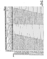
- the active-level duration during a reference period of the output signal or the terminal OUT (in Fig. 1, the reference perid corresponds to the count-end period of the down-counter) varies as shown in Fig. 2, corresponding to a change of the digital input. values, the active-level duration being shown by hatching Fig. 2.
- reference CL designates a clock pulse signal waveform
- Q7, Q6, Q5, Q4, Q3, Q2 and Ql designate output signal waveforms of T flip-flops 7, 6, 5, 4, 3, 2 and 1 in Fig. 1 respectively.
- the analog voltage corresponding to the digital input value is obtained from a low-pass filter or the like which is supplied the output signal on the terminal OUT.
- the reference period when increased to an extent of not sensing the flickering, can change the intensity of illumination, even without using the low-pass filter or the like, corresponding to the digital input value.
- the digital-to-analog convertor shown in Fig. 1 also cannot be expected of its desired function because of generation of. a hazard (glitch) in its circuit as original.
- a signal transfer delay occurs inevitably between the input and the output of each flip-flop in Fig. 1 to result in that the coincident detection by AND gate 18, during the transition of output of each flip-flop, will generate an erroneous output.
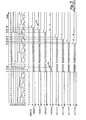
- Fig. 3 is a timing chart for explanation of the above, 'which is the same in a main point as that in Fig. 2, but is enlarged of the axis of time in comparison with Fig. 2, and the transfer delay having a time equal to 1/6 of the clock pulse period occurs in each flip-flop, but AND gates 8 and 18 and EX-OR gates 11 to 17, for the convenience, are negligible of the tranfer delay.
- an output of the down-counter becomes [0000000] and AND gate 8 generates a set signal for RS flip-flop 10 as shown by the signal waveform S in Fig. 3.
- the level change of an output terminal Q of RS flip-flop 10 delays by 1/6 of one clock period from the time t 1 and turns to "1", then delays by 1/6 of one clock period from the time t 10 and turns to "0"
- the level of output terminal Q e at RS flip-flop 10 turns to "1" after a delay from the time t 1 by . 1/6 of one clock period, and turns to "0" after the delay from t 8 .
- the level of output terminal Qe at RS flip-flop 10 turns to "1" after delay from the time t 1 , then after turns to "0" by the delay from the time t 8 .
- the active level duration dueto decrease by every one clock period, but only by 5/6 clock period between the digital input values [1000011] and [1000010] and by 7/6 clock period between the digital input values [1000010] and [1000001], in which an error of 1/6 clock period is created in both cases.
- the digital-to-analog converter in Fig. 1 makes a transfer error corresponding to a delay time for signal transfer at the T flip-flop constituting the down-counter.
- the hazard when [1000000] is applied as the digital input value, leads to a malfunction in the apparatus Since the output of the down-counter instantaneously becomes [01111111 at the time t 3 , a hazard h2 is applied to a reset terminal R of RS flip-flop 10, in the result the output level of the RS flip-flop turns to "0" and its output signal far different from the original waveform.
- the counter comprising T flip-flops 1 to 7 is made of synchronous type and of a high speed type and a hazard appearance region.is kept within at least 1/2 clock period from the leading edge of the clock pulse, and thereafter the synchronized output of the digital comparator is picked up at the trailing edge of the clock pulse.
- the portions surrounded by the broken line in Fig. 1 for example in a servo system of a video tape recorder disclosed in the aforesaid paper I E EE , will require four channels for speed control and phase control for a capstan motor and those for a cylinder motor, but the portion must be employed all high-speed gates for preventing a malfunction.
- the whole system is intended to be one-chip-IC, many problems have occured by increased consumption power and increased chip size.
- An object of the invention is to provide a digital-to-analog conversion apparatus with high-speed response.
- Another object of the invention is to provide a digital-to-analog conversion apparatus simplier in construction, in turn smaller in the number of gates, than this kind of conventional apparatus.
- the digital-to-analog conversion apparatus is so constructed that a counter for scaling clock pulses and a decoding-gate for generating an output pulse having a binary-weited duration, generate an output signal which varies the sum of the active-level duration, thereby being capable of operating stably up to high frequency with an extremely small number of gates and of saving the consumption power.
- Fig. 1 is a logic diagram of an exemplary construction of a conventional digital-to-analog converter
- Figs. 2 and 3 are timing charts explanatory of operation of the F ig. 1 converter
- Fig. 4 is a logic diagram of.an embodiment of a digital-to-analog conversion apparatus of the invention
- Figs. 5 through 7 are timing charts explanatory of operation of the Fig. 4 embodiment.
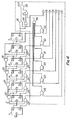
- F ig. 4 is a logic diagram of an embodiment of a digital to-analog conversion apparatus of the invention, in which T flip-flops 1 to 7, as the same as Fig. 1, constitute 7-bit down counter, an inverted output terminal Q 6 of T flip-flop 6 and an non-inverted output terminal Q 5 .
- T flip-flop 5 being connected to input terminals of an AND gate 19, an output terminal thereof and a non-inverted output terminal Q 4 of T flip-flop 4 being connected to input terminals of an AND gate 20, an output terminal thereof and a non-inverted output terminal Q 3 of T flip-flop'3 being connected to input terminals of an AND gate 21, and an output terminal thereof and an non-inverted output terminal Q 2 .of T flip-flop 2 being connected to input terminals of AND gate 22.
- An output terminal of AND gate 22 and an inverted output terminal Q 1 of T flip-flop 1 are connected to input terminals of an AND gate 23, an output terminal of AND gate 21 and an inverted output terminal Q 2 of T flip-flop 2 being connected to input terminals of an AND gate 24, an output terminal of AND gate 20 and an inverted output terminal Q 3 of T flip-flop 3 being connected to input terminals of an AND gate 25, an output terminal of AND gate 19 and an inverted output terminal Q 4 of T flip-flop 4 being connected to input terminals of an AND gate 26, and an inverted output terminal Q 6 of T flip-flop 6 and an inverted output terminal Q 5 of T flip-flop 5 being connected to input terminals of an AND gate 27.
- an output terminal of AND gate 23 and a digital input terminal D l are connected to input terminals of a NAND gate 28, an output terminal of AND gate 24 and a digital input terminal D 2 being connected to input terminals of a NAND gate 29, an output terminal of AND gate 25 and a digital input terminal D 3 being connected to input terminals of a NAND gate 30, an output terminal of AND gate 26 and a digital input terminal D 4 being connected to input terminals of a NAND gate 31, an output terminal of AND gate 27 and a digital input terminal D 5 being connected to input terminals of a NAND gate 32, a non-inverted output terminal Q 6 and a digital input terminal D 6 being connected to input terminals of a NAND gate 33, and output terminals of NAND gates 28 to 33 being connected to input terminals of an AND gate 34 respectively.
- an inverted output terminal Q7 of T fiip-flop 7 and a digital input terminal D 7 are connected to input terminals of a NAND gate 35 and a NOR gate 36 respectively, an output terminal of NOR gate 36 and an output terminal of AND gate 34 being connected to input terminals of an OR gate 37, an output terminal of NAND gate 35 and an output terminal of OR gate 37 being connected to input terminals of an AND gate 38, and an output terminal of AND gate 38 being connected to a signal output terminal OUT.
- AND gate 23 constitutes a first decoding gate which generates an output signal when the 7-bit down-counter comprising T flip-flops 1 to 7 outputs [x011110] (x designates irrelative level).
- AND gate 24 constitutes a second decoding gate which generates an output signal when the down-counter outputs [x01110x];
- AND gate 25 a third decoding gate generating an output signal when the output of the down-counter becomes [x0110xx];
- AND gate 26 a fourth decoding gate generating an output signal when the output of the down-counter becomes [x010xxx];
- AND gates 19, 20, 21 and 22 constitute auxiliary gates for decoding gates 23 to 27 respectively.
- the first decoding gate 23 twice generates the outputsignals when the down-counter outputs [1011110] and [0011110], one output duration being equal to a clock pulse period.
- the second decoding gate 24 twice generates the output signals when the output of down-counter is given between [1011101] and [1011100] and between [0011101] and [0011100], one output duration being equal to two times the clock pulse period.
- the third decoding gate 25 generates the output signals twice when the output of the down-counter is given between [1011011] and [1011000] and between [00110111 and [0011000], one output duration being equal to four times the clock pulse period.
- the fourth decoding gate 26 generates the output signals twice when the output of the down-counter is given between [101 0 111] ] and [1010000] and between [0010111] and [0010000], one output duration being equal to eight times the clock pulse period.
- the fifth decoding gate 27 generates the output signals twice when the output of the down-counter is given between [10011117] and [1000000] and between [0001111] and [0000000], one output duration being equal to sixteen times the clock pulse period.
- the second decoding gate 24 is binary-weighted for its output duration with respect to the first decoding gate 23, and similarly, the third, fourth, and fifth decoding gates 25, 26 and 27 are binary weighted for output durations thereof with respect to the second, third, and fourth decoding gates 24, 25 and 26 respectively.
- NAND gates 28, 29, 30, 31, 32 and 33 consititute logical AND gates generating output signals when levels of both input terminals of the NAND gates turn to "1", AND gate 34 constituting a negative logical OR gate, which generates an output signal when the level of either one input terminal of the AND gate 24 turns to "0".
- NAND gate 35, NOR gate 36, OR gate 37 and AND gate 38 constitute a selection gate which decides an effective active region of AND gate 34 corresponding to a level of MSB in the digital input value.
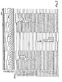
- the active level duration of the output signal when the digital input values are changed in variety, changes as shown in Fig. 5, and that during the reference period changes corresponding to a change of the digital input values.
- Fig. 6 shows the output signal waveforms for varying the digital input values, assuming that in each flip-flop a transfer delay having a time equal to 1/6 of the clock pulse period will occur.
- the output waveform when [1001111] is applied as the digital input value, is affected by the transfer delay as hazards h 3 , h 4 and h 5 as shown in Fig. 6-A.
- the apparatus of the invention triggers no flip-flop by the decoded output of the counter as the conventional apparatus in Fig. 1, whereby these hazards cause no malfunction and no conversion error as discussed below.
- the active level duration when [1001000] is applied as the digital input value, increases surely to an extent of seven clock pulse period with respect to that in Fig. 6-A.
- the duration increases surely to an extent of two clock pulse period with respect to Fig. 6-C when [1000010] is applied.
- one clock pulse period further increases when [000001] is applied and the same period further increases when [1000000] is applied.
- the output signal is affected by hazards h 6 , h 7 , h 8 , h9, hl0, and hll (not shown), and a pulse width of each hazard corresponds to a transfer delay time of each flip-flop to thereby become one clock pulse period from six hazards. Consequently, the active level duration increases by one clock pulse period with respect to Fig. 6-F.
- the active level duration when [0111110] is applied for digital input value, increases further by one clock pulse period, further by one clock pulse period when [0111101] is applied, further by two clock pulse period when [0111011] is applied, further by four clock pulse period when [0110111] is applied, and further by eight clock pulse period when [0101111] is applied (see Figs. 6-I, -J, --K and -L).
- the digital-to-analog conversion apparatus of the invention need not use, as particular countermeasures to hazards, a synchronous counter of a high speed type as conventional, so as to completely eliminate the conversion error caused by the transfer delay as well as malfunction. Accordingly, the apparatus of the invention, when using high speed gates as the same as the conventional one, can be used up to a high frequency only by a difference in the limit frequencies between the synchronous counter and a ripple counter,-and when operated in the frequency about equal to the conventional apparatus, can actually reduce the number of gates and save the consumption power.
- the block surrounded by the broken line in Fig. 1, as abovementioned, is normal to provide several. channels.
- the appara- .tus of the invention in Fig. 4 can be composed of a far smaller number of gates due to the fact that the EX-OR gate generally comprises four NAND gates.
- Figs. 3 and 6 assume that each flip-flop makes a transfer delay by a 1/6 clock pulse period, but actually, it is often used in the frequency in closer proximity to the limit. Especially in I 2 Z-IC or the like suitable to this kind of system, a method is taken which reduces an injection current as the ripple counter becomes a higher order, thereby saving the consumption power.
- the digital-to-analog apparatus of the invention also functions stably without occurence of any conversion error.
- Fig. 7 shows the output waveforms for varying the digital input values, assuming that in each flip-flop a transfer delay having a time equal to 1/4 of the triggering signal period, from which it is seen that the active-level duration, also from which it is seen that active-level duration also in.the above case, changes accurately corresponding to a change of the digital input value.
- Fig. 7-I shows an output signal waveform when [1000000] is applied, in which the active-level duration is just 1/2 of the counting period of the 7-bit down-counter.
- the digital input numeral decreases by 1 and becomes [0111111]
- hazards of 1/2 clock pulse period occur at two portions to increase the active level duration by one clock pulse period (see F ig. 7-J)
- the digital input value becomes [0111110] pulse widths of hazards apparently at two portions each become one clock pulse period, thereby further increasing the duration by one clock pulse period (see Fig. 7-K).
- the digital-to-analog conversion apparatus of the invention even if a reference counter .(7-bit down-counter in the Fig. 4 embodiment) and peripheral gates are considerably larger in a transfar delay, is simple in construction and performable in high accuracy without occurence of a malfunction or a conversion error, as far as the reference counter keeps its function as the counter.
- Fig. 4 shows the logic diagram of the embodiment of the invention designed thoroughly along the essence of the invention, .in which the constitution of decoding gates or its decoding method, may alternatively be, for example, of a ROM type (an increased bit number will make it effective from the- design of IC 'layout to adopt the ROM type), or the counter is not defined to the ripple or down counter, so that a synchronous counter may be used including the use of a dividing counter provided for other purposes.
- a synchronous counter may be used including the use of a dividing counter provided for other purposes.
- NAND gate 35, NOR gate 36, OR gate 37, and AND gate 38 are so constituted that the output of AND gate 34 which constitutes an logical OR gate in the negative logic, when MSB D 7 of the digital input value is at one level "1", becomes effective for one level "1" of MSB (Q 7 ) at the counter (the level “1" in Fig. 4 alternatively may be "0"), and, when MSB of digital input value is at the other level "0", becomes effective for the other level "0" of MSB at the counter.
- MSB at the digital input value. is at one level "I"
- an output signal from logical AND of the outputs of the counter in the Fig.
- the output of T flip-flop 7) and AND gate 34 is obtained, and when MSB at the digital input value is at the other level "0", an output signal by logical OR of the outputs of the counter and AND gate 34 is obtained.
- the reason for the above is that, throughly in consideration of the transient characteristic of the whole system, the constitution is designed so that no abrupt change occurs in the output signal waveform when the digital input.value changes from [1000000] to [0111111].
- the apparatus may be so constituted that the output of AND gate 34 is effective always when MSB at the counter is "1" or "0", which may be rather simple in circuitry.
Landscapes
- Engineering & Computer Science (AREA)
- Theoretical Computer Science (AREA)
- Analogue/Digital Conversion (AREA)
Applications Claiming Priority (2)
| Application Number | Priority Date | Filing Date | Title |
|---|---|---|---|
| JP16517/81 | 1981-02-05 | ||
| JP56016517A JPS57131124A (en) | 1981-02-05 | 1981-02-05 | Digital-to-analog converter |
Publications (3)
| Publication Number | Publication Date |
|---|---|
| EP0058064A2 true EP0058064A2 (de) | 1982-08-18 |
| EP0058064A3 EP0058064A3 (en) | 1984-06-20 |
| EP0058064B1 EP0058064B1 (de) | 1987-12-02 |
Family
ID=11918459
Family Applications (1)
| Application Number | Title | Priority Date | Filing Date |
|---|---|---|---|
| EP82300587A Expired EP0058064B1 (de) | 1981-02-05 | 1982-02-05 | Digital-Analog-Umwandlungsgerät |
Country Status (4)
| Country | Link |
|---|---|
| US (1) | US4473819A (de) |
| EP (1) | EP0058064B1 (de) |
| JP (1) | JPS57131124A (de) |
| DE (1) | DE3277794D1 (de) |
Families Citing this family (1)
| Publication number | Priority date | Publication date | Assignee | Title |
|---|---|---|---|---|
| US5774080A (en) * | 1994-12-15 | 1998-06-30 | Analog Devices, Incorporated | Reduced transistor-count data storage and multiplexing system |
Family Cites Families (6)
| Publication number | Priority date | Publication date | Assignee | Title |
|---|---|---|---|---|
| US3603977A (en) * | 1969-06-19 | 1971-09-07 | Westinghouse Electric Corp | Digital-to-analog converter utilizing pulse duration modulation |
| JPS5190552A (en) * | 1975-02-06 | 1976-08-09 | d*a henkankairo | |
| JPS5228205A (en) * | 1975-08-28 | 1977-03-03 | Sony Corp | Station selector unit |
| US4126853A (en) * | 1975-11-05 | 1978-11-21 | Rockwell International Corporation | Non-linear digital-to analog conversion |
| JPS547263A (en) * | 1977-06-20 | 1979-01-19 | Hitachi Ltd | D-a converter |
| FR2398415A1 (fr) * | 1977-07-21 | 1979-02-16 | Ibm | Convertisseur numerique-analogique |
-
1981
- 1981-02-05 JP JP56016517A patent/JPS57131124A/ja active Granted
-
1982
- 1982-02-04 US US06/345,919 patent/US4473819A/en not_active Expired - Lifetime
- 1982-02-05 EP EP82300587A patent/EP0058064B1/de not_active Expired
- 1982-02-05 DE DE8282300587T patent/DE3277794D1/de not_active Expired
Also Published As
| Publication number | Publication date |
|---|---|
| US4473819A (en) | 1984-09-25 |
| JPS6211820B2 (de) | 1987-03-14 |
| JPS57131124A (en) | 1982-08-13 |
| DE3277794D1 (en) | 1988-01-14 |
| EP0058064B1 (de) | 1987-12-02 |
| EP0058064A3 (en) | 1984-06-20 |
Similar Documents
| Publication | Publication Date | Title |
|---|---|---|
| US3422423A (en) | Digital-to-analog converter | |
| JPS6143899B2 (de) | ||
| US4118791A (en) | Multi-level encoding system | |
| EP0058064A2 (de) | Digital-Analog-Umwandlungsgerät | |
| US4521898A (en) | Ripple counter circuit having reduced propagation delay | |
| CA1089568A (en) | Digital-to-analog converter | |
| US4837573A (en) | Digital to analog converter | |
| JPS6245217A (ja) | パルス幅変調回路 | |
| US5272461A (en) | Coding circuit | |
| JP3036869B2 (ja) | Ad変換回路 | |
| US4180797A (en) | Digital comparator constructed of IIL | |
| KR930010940B1 (ko) | 입력인지 회로 | |
| JPS58161530A (ja) | A/d変換回路 | |
| JP2803231B2 (ja) | エミッタフォロア回路 | |
| JPS6324577B2 (de) | ||
| JPS6196811A (ja) | 信号変換回路 | |
| JPS5811133B2 (ja) | フリツプフロツプ回路 | |
| JP2643967B2 (ja) | サーボ回路 | |
| JPS60200624A (ja) | デイジタル記録信号再生装置 | |
| JPH0466133B2 (de) | ||
| JPH0642625B2 (ja) | パルス発生回路 | |
| JPS61251328A (ja) | Pwm回路 | |
| JPS62286Y2 (de) | ||
| JPH0645886A (ja) | パルス幅変調回路 | |
| JPS59100615A (ja) | 波形整形回路 |
Legal Events
| Date | Code | Title | Description |
|---|---|---|---|
| PUAI | Public reference made under article 153(3) epc to a published international application that has entered the european phase |
Free format text: ORIGINAL CODE: 0009012 |
|
| AK | Designated contracting states |
Designated state(s): DE FR GB |
|
| PUAL | Search report despatched |
Free format text: ORIGINAL CODE: 0009013 |
|
| AK | Designated contracting states |
Designated state(s): DE FR GB |
|
| 17P | Request for examination filed |
Effective date: 19841219 |
|
| GRAA | (expected) grant |
Free format text: ORIGINAL CODE: 0009210 |
|
| AK | Designated contracting states |
Kind code of ref document: B1 Designated state(s): DE FR GB |
|
| REF | Corresponds to: |
Ref document number: 3277794 Country of ref document: DE Date of ref document: 19880114 |
|
| ET | Fr: translation filed | ||
| PLBE | No opposition filed within time limit |
Free format text: ORIGINAL CODE: 0009261 |
|
| STAA | Information on the status of an ep patent application or granted ep patent |
Free format text: STATUS: NO OPPOSITION FILED WITHIN TIME LIMIT |
|
| 26N | No opposition filed | ||
| PGFP | Annual fee paid to national office [announced via postgrant information from national office to epo] |
Ref country code: GB Payment date: 19980127 Year of fee payment: 17 |
|
| PGFP | Annual fee paid to national office [announced via postgrant information from national office to epo] |
Ref country code: FR Payment date: 19980210 Year of fee payment: 17 |
|
| PGFP | Annual fee paid to national office [announced via postgrant information from national office to epo] |
Ref country code: DE Payment date: 19980213 Year of fee payment: 17 |
|
| PG25 | Lapsed in a contracting state [announced via postgrant information from national office to epo] |
Ref country code: GB Free format text: LAPSE BECAUSE OF NON-PAYMENT OF DUE FEES Effective date: 19990205 |
|
| GBPC | Gb: european patent ceased through non-payment of renewal fee |
Effective date: 19990205 |
|
| PG25 | Lapsed in a contracting state [announced via postgrant information from national office to epo] |
Ref country code: FR Free format text: LAPSE BECAUSE OF NON-PAYMENT OF DUE FEES Effective date: 19991029 |
|
| PG25 | Lapsed in a contracting state [announced via postgrant information from national office to epo] |
Ref country code: DE Free format text: LAPSE BECAUSE OF NON-PAYMENT OF DUE FEES Effective date: 19991201 |
|
| REG | Reference to a national code |
Ref country code: FR Ref legal event code: ST |