EP0055539B1 - Treiberkreis für Wärmedrucker und damit ausgestatteter Wärmedrucker - Google Patents
Treiberkreis für Wärmedrucker und damit ausgestatteter Wärmedrucker Download PDFInfo
- Publication number
- EP0055539B1 EP0055539B1 EP81305790A EP81305790A EP0055539B1 EP 0055539 B1 EP0055539 B1 EP 0055539B1 EP 81305790 A EP81305790 A EP 81305790A EP 81305790 A EP81305790 A EP 81305790A EP 0055539 B1 EP0055539 B1 EP 0055539B1
- Authority
- EP
- European Patent Office
- Prior art keywords
- circuit
- voltage drop
- constant voltage
- voltage
- capacitor
- Prior art date
- Legal status (The legal status is an assumption and is not a legal conclusion. Google has not performed a legal analysis and makes no representation as to the accuracy of the status listed.)
- Expired
Links
- 239000003990 capacitor Substances 0.000 claims description 39
- 238000007599 discharging Methods 0.000 claims description 8
- 238000010586 diagram Methods 0.000 description 10
- 230000007423 decrease Effects 0.000 description 9
- 230000003247 decreasing effect Effects 0.000 description 6
- 238000010438 heat treatment Methods 0.000 description 6
- PWHULOQIROXLJO-UHFFFAOYSA-N Manganese Chemical compound [Mn] PWHULOQIROXLJO-UHFFFAOYSA-N 0.000 description 4
- 229910052748 manganese Inorganic materials 0.000 description 4
- 239000011572 manganese Substances 0.000 description 4
- 230000009467 reduction Effects 0.000 description 4
- 230000033001 locomotion Effects 0.000 description 3
- 238000012545 processing Methods 0.000 description 3
- 230000005540 biological transmission Effects 0.000 description 2
- 229910010293 ceramic material Inorganic materials 0.000 description 2
- 239000011159 matrix material Substances 0.000 description 2
- 230000001681 protective effect Effects 0.000 description 2
- XUIMIQQOPSSXEZ-UHFFFAOYSA-N Silicon Chemical compound [Si] XUIMIQQOPSSXEZ-UHFFFAOYSA-N 0.000 description 1
- 230000008901 benefit Effects 0.000 description 1
- OJIJEKBXJYRIBZ-UHFFFAOYSA-N cadmium nickel Chemical compound [Ni].[Cd] OJIJEKBXJYRIBZ-UHFFFAOYSA-N 0.000 description 1
- 230000008859 change Effects 0.000 description 1
- 238000012937 correction Methods 0.000 description 1
- 230000004048 modification Effects 0.000 description 1
- 238000012986 modification Methods 0.000 description 1
- 238000011112 process operation Methods 0.000 description 1
- 238000009877 rendering Methods 0.000 description 1
- 238000007493 shaping process Methods 0.000 description 1
- 229910052710 silicon Inorganic materials 0.000 description 1
- 239000010703 silicon Substances 0.000 description 1
Images



Classifications
-
- B—PERFORMING OPERATIONS; TRANSPORTING
- B41—PRINTING; LINING MACHINES; TYPEWRITERS; STAMPS
- B41J—TYPEWRITERS; SELECTIVE PRINTING MECHANISMS, i.e. MECHANISMS PRINTING OTHERWISE THAN FROM A FORME; CORRECTION OF TYPOGRAPHICAL ERRORS
- B41J2/00—Typewriters or selective printing mechanisms characterised by the printing or marking process for which they are designed
- B41J2/315—Typewriters or selective printing mechanisms characterised by the printing or marking process for which they are designed characterised by selective application of heat to a heat sensitive printing or impression-transfer material
- B41J2/32—Typewriters or selective printing mechanisms characterised by the printing or marking process for which they are designed characterised by selective application of heat to a heat sensitive printing or impression-transfer material using thermal heads
- B41J2/35—Typewriters or selective printing mechanisms characterised by the printing or marking process for which they are designed characterised by selective application of heat to a heat sensitive printing or impression-transfer material using thermal heads providing current or voltage to the thermal head
- B41J2/355—Control circuits for heating-element selection
Definitions
- This invention relates to thermal printer drive circuits and to thermal printers provided therewith.
- a drive circuit for a thermal printer which prints characters on a printing medium by selectively applying current to a plurality of heat generating elements, comprising current application control means for controlling the application of current to the heat generating elements, and a time control circuit capable of varying the period of time for which the current application control means is rendered operative, the time control circuit including a charging circuit which is a series circuit connected between the terminals of a power supply from which current is provided to the heat generating elements and which includes a constant voltage drop means, a resistance means and a capacitor, a discharging circuit connected in parallel to the capacitor, and a voltage comparison circuit for switching the current application control means off when the charge on the capacitor has reached a reference value.
- the reference value is an external constant voltage source, resulting in disadvantages explained below in connection with a conventional constant temperature control circuit for a thermal pen disclosed in JP-A-53/ 15378 and illustrated herein in Figures 1 to 3.
- the present invention is characterised in that the constant voltage drop means is a first constant voltage drop means and is included in a first voltage divider circuit across the terminals of the power supply, which also includes a resistance means, the capacitor of the charging circuit being connected through the resistance means thereof to an intermediate point of the divider circuit, so that said capacitor is charged by the voltage drop across the resistance means and the voltage comparison circuit includes a second constant voltage drop means connected in series with a resistance means across the terminals of the power supply, the second constant voltage drop means providing the reference value for comparison with that of the capacitor.
- the resistance means of the divider circuit includes a third constant voltage drop means connected in series between the intermediate point and the other terminal of the power supply.
- thermo printer having a drive circuit as recited above.
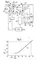
- Figure 1 shows a part of a conventional constant temperature control circuit for a thermal pen, which has been disclosed in Japanese Patent Application Publication No. 15378/1978 and is similar to the drive circuit in accordance with the preamble of claim 1. If the circuit shown in Figure 1 is modified somewhat, then it can be applied to a thermal printer.
- This conventional constant temperature control circuit has a power source 1, such as a battery, whose output or supply voltage Vc varies with time, a resistor 2, and a capacitor 3.
- the capacitor 3 is connected in series with the power source 1 through the resistor 2.
- a switch 4 is connected in parallel with the capacitor 3.
- the resistor 2, the capacitor 3 and the switch 4 form a charge- discharge circuit 11.
- a switch drive circuit 5 operates (opens and closes) the switch 4 at a predetermined times.
- the conventional constant temperature control circuit also has a voltage comparison circuit 6, an external reference power source 7, a variable voltage divider 8, a thermal pen 9 and a switch 10 for the thermal pen.
- the switch 10 is turned on and off by the output of the voltage comparison circuit, so as to maintain the temperature of the thermal pen 9 constant irrespective of variation of the supply voltage Vc.
- the operating principle that the heat generating elements are heated to a predetermined temperature to obtain a constant print quality is equally applicable to this case.
- the capacitor 3 is discharged by momentarily closing the switch 4, a period of time t required for charging the capacitor to a voltage E, which is obtained by applying the voltage from the reference power source 7 to the variable voltage divider 8, is detected by means of the voltage comparison circuit 6, and the switch 10 is closed for a heating period t within a predetermined period T to a control the temperature of the thermal pen 9.
- FIG. 2 is a diagram showing the relationship of the heating period t with the supply voltage Vc.
- V the supply voltage
- the charging time is relatively short and accordingly the heating period is relatively short as indicated by t l .
- the supply voltage is relatively low as indicated by V 2
- the charging time is relatively long and accordingly the heating period is relatively long as indicated by t 2 .
- the resistance of the thermal pen 9 is represented by r
- energy per unit time P w applied to the thermal pen can be represented by the following equation:
- the energy P w should be maintained constant.
- the relation between t and Vc is' as follows: This relationship will be referred to as "an equal energy characteristic” and “an equal temperature characteristic” hereinafter.
- the heating period t can be represented by the following equation:
- Figure 3 is a logarithmic graphical representation with Vc/E as the x-axis and with t/CR as the y-axis.
- curve 31 is obtained by dividing equation (3) by CR.
- Reference numeral 32 designates a straight line having a slope of (-2).
- the locus of a point which is parallel with the straight line 32 can be represented by the following equation: where a is a constant.
- the relation (2) between t and Vc of the equal temperature characteristic is equivalent to equation (4), and the temperature is maintained unchanged with the locus parallel with the straight line 32.
- a manganese dry cell SUM-3 has an internal resistance of about 0.5f2. Therefore, in the case where, as in a thermal printer, a plurality of heat generating elements each corresponding to the thermal pen 9 are supplied with current simultaneously, the supply voltage Vc falls markedly, and therefore it is necessary to use a circuit which exhibits the equal energy characteristic over a wider range of voltages. In a system in which, similarly to that of a thermal printer, energy is converted into heat instantaneously to form dots, even a small energy difference greatly affects the print quality, and accordingly a characteristic closer to the straight line 32 is required. In addition, the direction of the curve 31 is such that excessive energy is provided for both high and low voltages.
- FIG. 4 there is shown an electronic desk calculator employing one embodiment of a thermal printer drive circuit according to the present invention.
- This electronic desk calculator has a battery or power source 41, a transistor 42 which acts as a switching device for supplying current to the thermal printer drive circuit, a transistor 43 for controlling the transistor 42, the transistor 42 being maintained non-conductive (off) when the thermal printer is not operated, a first constant voltage drop device or Zener diode 44, a resistor 45 and a diode 46.
- the Zener diode 44, the resistor 45 and the diode 46 form a voltage divider circuit 47 for dividing a supply voltage Vc from the power source 41.
- a capacitor 50 is connected through a variable resistor 48 to the point S which is a voltage divider point of the voltage divider circuit 47 across the power source 41.
- a discharging circuit made up of a protective resistor 51 and a transistor 52 is connected in parallel with the capacitor 50.
- the voltage at the point S is indicated by Vs hereinafter.
- a voltage comparison circuit 53 acts as a switching circuit which is turned on and off according to the charge on the capacitor 50.
- a reference voltage E is developed across a second constant voltage drop means in the form of a Zener diode 54 connected in series with a resistor 55.
- the reference voltage E and the voltage level of the capacitor 50 are compared by the voltage comparison circuit 53, and according to the result of the comparison, the output of the voltage comparison circuit 53 is changed.
- the output of the voltage comparison circuit 53 is logic O.
- the period of time for applying current to heat generating elements 60 of the thermal printer is determined by the supply voltage.
- the elements described above form a current application time control circuit which is generally indicated at 56 in Figure 4.
- a heat generating head 61 is made of ceramic material and incorporates the heat generating elements 60.
- 5x7 matrix characters are formed with dots by moving the heat generating head 61 laterally, the heat generating elements 60 being arranged to correspond to seven dots arranged longitudinally.
- a transistor 63 which acts as a current application control device is used to control the application of current to the heat generating elements 60.
- a central processing unit (CPU) 64 is provided for processing operation and for controlling the thermal printer.
- a character signal generating circuit 65 is coupled to the CPU. In the case where a microprocessor is employed as the CPU, in general, an input/output (I/O) port is used.
- Figure 5 is a graphical representation indicating the variation of supply voltage Vc with potential Vs at the point S of the voltage divider circuit 47.
- the Zener diode 44 has a maximum Zener voltage V z of 2.5V for example.
- the diode 46 is a silicon diode having a maximum voltage of about 0.7V. The forward voltage of the diode 46 is scarcely altered even when the supply voltage Vc is decreased and the current flowing in the diode 46 is decreased. Therefore a characteristic curve 70 is obtained in Figure 5.
- the potential Vs at the point S is an actual charging potential of the capacitor 50.
- the potential at the point S can be approximated by the following expression:
- the output pulse width (t) of the voltage comparison circuit 53 can be represented by the following equation: where C is the capacitance of the capacitor 50, and R is the resistance of the variable register 48. It should be noted that the output pulse width can be substantially represented by equation (6) in the case where the diode 46 is omitted. However, it is represented by the following equation in the case where the diode 46 is provided:
- the reference voltage E is 0.7V in the case where the supply voltage Vc is approximately 6.4V and is 0.6V in the case where the supply voltage Vc is approximately 3.6V.
- like parts are designated by the same reference numerals.
- curve 71 is of the current application time control circuit 56 using the voltage divider circuit 47.
- a region from point J to point K of the curve 71 corresponds to the range of x from 6.0 to 9.2 and the points lie on a line 72 parallel with the straight line 32 having a slope of (-2).
- This means that the equal energy characteristic range is greatly increased when compared with that of the conventional constant temperature control circuit. In other words, even if the capacity of the power source 41 decreases and accordingly its output voltage decreases, suitable power is applied to the heat generating elements 60 and printing is produced with suitable density.
- a curve 73 indicated by a broken line in Figure 6 illustrates the case where the diode 46 is omitted.
- a region of the curve 73 which corresponds to a range of X from 6.8 to 9.2, is substantially in approximation with the straight line 72, and therefore the applicable range of voltages is wider than that of the curve 31.
- This curve 73 is sufficient for a dry cell, such as a nickel-cadmium dry cell, having a relatively small range of variation of supply voltage.
- the current application time control circuit 56 may be modified in such a manner that the resistor 45 is omitted, and a series circuit of the Zener diode 44, the variable resistor 48 and the capacitor 50 is connected to the power source 41. In this modification, a curve substantially similar to the curve 73 is obtained.
- the drive circuit for the thermal printer of Figure 4 has the advantage that, as the current application time is increased with reduction in supply voltage, power is economically consumed substantially at all times.
- FIG. 7 is a circuit diagram showing an electronic desk calculator having a second embodiment of a thermal printer drive circuit according to the present invention.
- a first constant voltage drop device is composed of a transistor 81, a resistor 82, and a resistor 83. If the resistor 83 (or the resistor 82) is a variable resistor the potential Vz may be adjusted.
- a transistor 84 is employed as a third constant voltage drop device.
- a diode 85 is connected between the point S in the voltage divider circuit 47 formed of the first and third constant voltage drop devices, and a variable resistor 48 is connected to the capacitor 50.
- the diode 85 is used when it is required to finely change the characteristics of the circuit and therefore it may be omitted.
- reference numeral 52 designates a discharging transistor.
- the protective resistor 51 in Figure 4 is omitted from the discharging transistor 52.
- a transistor 86 is employed instead of the voltage comparison circuit 53 in Figure 4, a transistor 86 is employed.
- the transistor 86 is rendered conductive when the charge on the capacitor 50 reaches the case-emitter voltage Vbe of the transistor 86.
- a load resistor 87 is connected to the collector of the transistor 86.
- the load resistor 87 and the transistor 86 form a voltage comparison circuit.
- the variation of the output pulse width of the transistor 86 due to the variation of the base-emitter voltage Vbe attributed to temperature variation coincides with the temperature characteristic of current application time for the heat generating elements 60, thus performing temperature compensation.
- the circuit elements described so far form a current application time control circuit 90.
- the output of the current application time control circuit 90 is applied through a buffer circuit 91 to a plurality of AND gates 92.
- the heat generating elements 60 incorporated in the heat generating head 61 are divided into two groups a and b which are offset in the direction A of movement of the heat generating head 61, so that the maximum of heat generating elements energised simultaneously is four.
- Character signal generating circuits 93, 94 are provided for the groups a and b of heat generating elements respectively.
- An electric motor 95 acts as the drive source of the thermal printer, the motor 95 being adapted to move the heat generating head 61 in the direction A or to feed a sheet of recording medium such as paper.
- a permanent magnet 96 is fixed to the shaft of the motor 95.
- the provision of the tachometer generator 98 guarantees equal dot intervals on the printing medium irrespective of the speed of the motor 95.
- the output of the tachometer generator 98 is shaped into a timing signal by a timing signal generating circuit 99, the timing signal being applied to the transistor 52 to render the latter conductive momentarily and to the CPU 64.
- the tachometer generator 98 and the timing signal generating circuit 99 from a position detector 100 which operates to detect print position.
- Figure 8 is a timing diagram of the thermal printer drive circuit shown in Figure 7.
- reference numeral 101 designates the output waveform of the tachometer generator 98, the sinusoidal waveform being generated in the coil of the magnetic head 97 as the motor is rotated
- reference numeral 102 designates the output waveform of the position detector 100, its pulse width being very small.
- the transistor 52 is rendered conductive and non-conductive repeatedly in synchronization with the period of the tachometer generator 98.
- the initial current application is at T o (a) in Figure 8, then at time T o (b) printing has been achieved for one line. Thereafter, the current application is at T,(a), T,(b) and so on to form a character.
- the output waveform of the transistor 86 of the current application time control circuit 90 is as indicated at 103 in Figure 8, and the pulse width varies with the supply voltage Vc.
- the pulse width (t) is increased to Tw,.
- the pulse width (t) is decreased to Tw 2 .
- the output waveform 103 and the character signal generating circuits 93, 94 are combined through the AND gates 92 to select the groups a and b of heat generating elements 60 to form desired characters.
- a temperature detecting element such as a thermistor (not shown) may be connected in series or in parallel to the variable resistor 48.
- thermal printer drive circuits shown in Figures 4 and 7 may be modified, the constant voltage devices being replaced by one or more diodes which are connected in series according to the value of the voltage Vz, with the forward characteristic of each diode being utilised.
- FIG. 9 is a perspective view of a thermal printer to which a thermal printer drive circuit according to the present invention is applied.
- An electric motor 110 is employed as the drive source.
- a reduction gear box 11 incorporates a reduction gear (not shown) which is engaged with the motor 110.
- a cam gear 112 engages with the reduction gear and operates together with a head feed cam 133.
- the head feed cam 113 has a groove 130.
- the groove 130 is engaged with a carriage 122 which supports a head 124.
- Reference numerals 114, 115 designate a clutch ratch wheel and a clutch gear, respectively.
- a clutch spring (not shown) incorporated in the clutch ratchet wheel 114, and the clutch gear, one reciprocating rotary motion per line of printing (as indicated by the arrow B) is transmitted to a sheet feed transmission gear 116.
- a sheet feed roller 119 is mounted on the sheet feed roller shaft to feed a sheet 131 of printing medium such as paper for every line of printing.
- a platen lever 120 is engaged with a cam 121 which is integral with the sheet feed transmission gear 116.
- the platen lever 120 is urged against the carriage 122 by a platen spring 126 in the printing operation, and is released in the returning operation.
- a platen 133 is fixed to the platen lever 120.
- the carriage 122 is reciprocated along a guide shaft 123 by the head feed cam 113.
- a print head 124 having heat generating elements 125 is fixed to the carriage 123.
- a flexible power cable (FPC) 127 is connected to the head 124.
- a tachometer generator 128 is engaged with the motor 110 to detect print positions.
- a reset position detector 132 is provided to detect a printing start position of the printing head.
- a thermal printer drive circuit according to the present invention is not only applicable to the thermal printer shown in Figure 9 but also to other types of thermal printers.
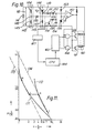
- FIG 10 is a schematic circuit diagram showing an electronic desk calculator having a third embodiment of a thermal printer drive circuit according to the present invention.
- This thermal printer drive circuit has a power source 141, for example a battery, a second voltage divider circuit 142 consisting of resistors 144, 145, and a first voltage divider circuit 143 including a Zener diode 146 which is a constant voltage drop device and a resistor 147.
- a voltage divider point 148 of the second voltage divider circuit is at a potential Vd of the power source 141 multiplied by a predetermined fraction (n).
- the first voltage divider circuit 143 utilises the characteristics of the Zener diode 146, that is at a point 149 a voltage Vd-Vz is provided (where Vz is the constant voltage drop of the Zener diode).
- Diodes 150, 151 are connected to the points 148, 149, respectively.
- the voltage divider circuits 142 and 143 are connected through the diodes 150 and 151 respectively, to a common connecting point 152 at the end of a variable resistor 153.
- a capacitor 154 is connected between the variable resistor 153 and one terminal of the power source 141.
- the second voltage divider circuit 142, the first voltage divider circuit 143, the diodes 150, 151, the adjusting resistor 153 and the capacitor 154 form a charging circuit.
- a discharging transistor 156 is connected in parallel with the capacitor 154 to control the charge and discharge of the latter.
- a voltage comparison circuit 157 which is a type of switching circuit, is turned on and off according to the charge on the capacitor 154.
- a reference voltage E is produced by a Zener diode 158 and a series-connected resistor 159.
- the charge on the capacitor 154 is compared with the reference voltage E in the voltage comparison circuit 157, and the output level of the comparison circuit 157 is changed according to the result of the comparison. More specifically, in Figure 10, when the charge on the capacitor 154 exceeds the reference voltage E, the output of the voltage comparison circuit 157 is set to-logic O.
- the elements described determine the current application time for the heat generating elements 160 of the thermal printer according to supply voltage and form a current application time control circuit.
- a heat generating head 161 made of, for example, ceramic material includes the heat generating elements 160.
- the heat generating elements 160 corresponding to 7 dots are aligned longitudinally in the heat generating head 161.
- a 5x7 matrix characters are formed with dots.
- a plurality of transistors 163 operate to control selectively the application of current to the heat generating elements 160.
- a central processing unit (CPU) 165 is provided to process operations and to control the thermal printer.
- a character signal generating circuit 165 is coupled to the CPU 164.
- the outputs of the character signal generating circuit 165 and the voltage comparison circuit 157 are applied to a plurality of AND gates 166, as a result of which the transistors 163 are rendered conductive for a period of time corresponding to the supply voltage Vd, and accordingly printing of desired density is produced.
- a timing signal generating circuit 167 operates to detect the position of the heat generating head 161 to generate a printing timing signal which renders the transistor 156 conductive momentarily.
- the period of time for which the transistor 156 is rendered conductive is from several to several tens of microseconds.
- Figure 11 is a graph showing the characteristics of the thermal printer drive circuit of Figure 10.
- the scale of Figure 11 is similar to that of Figure 3.
- a curve 171 is the same as the characteristic curve of the conventional constant temperature control circuit as shown in Figure 3.
- the curve 171 can be represented by the following equation: where, C is the capacitance of the capacitor 154, and R is the resistance of the variable resistor 153.
- the value t is y ⁇ C ⁇ R. and represents the period of time for which the transistor 163 is rendered conductive.
- curve 172 is obtained when only the first voltage divider circuit 143 is taken into account.
- the value t can be represented by the following equation:
- Straight lines 173, 174 in Figure 11 have a slope of (-2).
- the voltage drop across the diodes 150, 151 can be theoretically disregarded, but in practice some correction is required.
- the thermal printer drive circuit of Figure 10 makes it possible to drive a thermal printer with a power source such as a manganese dry cell having a wide range of voltage variation and efficiently to use the capacity of the dry cell to the full.
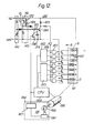
- FIG 12 is a schematic circuit diagram of an electronic desk calculator having a fourth embodiment of a thermal printer drive circuit according to the present invention.
- the second voltage divider circuit 142 in Figure 12 is completely identical to that in Figure 10.
- the first voltage divider circuit 143 has a transistor 181 and resistors 182, 183, and utilises the constant voltage characteristics of a transistor. Therefore, if a variable resistor is employed as the resistor 183 (or the resistor 182), then the voltage Vz can be adjusted so that the characteristic can be changed.
- the voltage comparison circuit the output of which is turned on or off according to the charge on the capacitor 154, is very simple being formed with a transistor 184 and a load resistor 185.
- a waveform shaping buffer circuit 186 is employed to apply the output of the thermal printer drive circuit to a plurality of AND gates 187.
- the reference voltage E is the base-emitter voltage (Vbe) of the transistor 184 and it is, in general, of the order of 0.7V.
- the temperature characteristic of the base-emitter voltage coincides with the temperature characteristic of the current application time for the heat generating elements 160, thus performing temperature compensation also. More specifically, at a low temperature the base-emitter voltage of the transistor 184 is increased and therefore the time required for charging the capacitor 154 is increased. On the other hand, when the temperature is high, the current application time is decreased. Thus, in either case, a suitable print quality can be obtained.
- the circuit elements described so far form a current application time control circuit 195.
- the heat generating elements 160 are divided into two groups a and b which are offset in the direction of movement A so that the maximum number of heat generating elements 160 energised simultaneously or the maximum number of dots printer simultaneously is four.
- Character signal generating circuits 192, 193 are provided for the groups a and b of heat generating elements, respectively.
- the thermal printer has a motor 188 as a drive source which moves the heat generating head 161 in the direction A and to operate the sheet feed unit (not shown).
- a permanent magnet 189 is fixed to the shaft of the motor 188.
- the permanent magnet 189 and a magnetic head 190 including a coil form a tachometer generator 191.
- the tachometer generator 191 produces a waveform for detecting the printing timing of the groups a and b of heat generating elements 160.
- the provision of the tachometer generator 191 guarantees equal dot intervals on a sheet of printing medium (not shown) irrespective of the speed of the motor 188.
- the output of the tachometer generator 191 is converted into a waveform for rendering the transistor 156 conductive momentarily by the timing signal generating circuit, and the output of the latter is applied to the CPU 164 also.
- the tachometer generator 191 and the timing signal generating circuit 167 form a position detector 194 adapted to detect a print position.
Landscapes
- Electronic Switches (AREA)
- Facsimile Heads (AREA)
- Accessory Devices And Overall Control Thereof (AREA)
Claims (14)
Applications Claiming Priority (2)
| Application Number | Priority Date | Filing Date | Title |
|---|---|---|---|
| JP55187626A JPS6036949B2 (ja) | 1980-12-29 | 1980-12-29 | サ−マルプリンタの駆動回路 |
| JP187626/80 | 1980-12-29 |
Publications (3)
| Publication Number | Publication Date |
|---|---|
| EP0055539A2 EP0055539A2 (de) | 1982-07-07 |
| EP0055539A3 EP0055539A3 (en) | 1983-07-27 |
| EP0055539B1 true EP0055539B1 (de) | 1986-07-16 |
Family
ID=16209395
Family Applications (1)
| Application Number | Title | Priority Date | Filing Date |
|---|---|---|---|
| EP81305790A Expired EP0055539B1 (de) | 1980-12-29 | 1981-12-08 | Treiberkreis für Wärmedrucker und damit ausgestatteter Wärmedrucker |
Country Status (4)
| Country | Link |
|---|---|
| US (1) | US4409600A (de) |
| EP (1) | EP0055539B1 (de) |
| JP (1) | JPS6036949B2 (de) |
| DE (1) | DE3174942D1 (de) |
Families Citing this family (21)
| Publication number | Priority date | Publication date | Assignee | Title |
|---|---|---|---|---|
| JPS58124678A (ja) * | 1982-01-20 | 1983-07-25 | Fuji Xerox Co Ltd | サ−マルヘツド駆動方式 |
| AU567487B2 (en) * | 1982-01-25 | 1987-11-26 | Sony Corporation | Thermal printer |
| JPS58150370A (ja) * | 1982-03-02 | 1983-09-07 | Sony Corp | プリンタにおける階調信号発生回路 |
| JPS58197063A (ja) * | 1982-05-13 | 1983-11-16 | Toshiba Corp | 印字ヘッド駆動方式 |
| US4542281A (en) * | 1984-03-02 | 1985-09-17 | Combustion Engineering, Inc. | Thermal printer contrast control |
| JPS60210473A (ja) * | 1984-04-04 | 1985-10-22 | Canon Inc | サ−マルヘツド駆動装置 |
| US4714363A (en) * | 1984-05-18 | 1987-12-22 | Seiko Epson Corporation | Print control device for a dot matrix printer |
| JPS615960A (ja) * | 1984-06-20 | 1986-01-11 | Ricoh Co Ltd | 非安定化電源を用いた感熱記録方式 |
| JPS61230962A (ja) * | 1985-04-08 | 1986-10-15 | Sato :Kk | サ−マルヘツドの温度制御装置 |
| JPS6237179A (ja) * | 1985-08-13 | 1987-02-18 | Oki Electric Ind Co Ltd | アラ−ム検出回路 |
| DE3620535A1 (de) * | 1986-06-19 | 1987-12-23 | Mannesmann Ag | Elektronische steuerschaltung, insbesondere fuer einen drucker |
| US5432533A (en) * | 1986-07-18 | 1995-07-11 | Canon Kabushiki Kaisha | Recording method with control of head energization and recording medium conveyance power consumption |
| US5191356A (en) * | 1986-07-18 | 1993-03-02 | Canon Kabushiki Kaisha | Tower conserving recording apparatus |
| US4717924A (en) * | 1986-08-18 | 1988-01-05 | Ncr Corporation | Thermal printing control system |
| JPH0611801Y2 (ja) * | 1986-12-24 | 1994-03-30 | 富士通株式会社 | サ−マルヘツド駆動装置 |
| DE58906957D1 (de) * | 1989-11-02 | 1994-03-24 | Siemens Ag | Verfahren zum betrieb einer von mindestens einem wiederaufladbaren akkumulator gespeisten aufzeichnungseinrichtung. |
| JP2993804B2 (ja) * | 1992-09-01 | 1999-12-27 | 富士写真フイルム株式会社 | サーマルヘッドの抵抗値測定方法及び装置並びにこれを備えたサーマルプリンタ |
| JP3013042B1 (ja) * | 1998-12-21 | 2000-02-28 | セイコーインスツルメンツ株式会社 | サーマルプリンタ装置 |
| US6799004B2 (en) * | 2002-09-19 | 2004-09-28 | Hewlett-Packard Development Company, L.P. | Imaging equipment acceleration apparatus and methods |
| US7197268B2 (en) * | 2005-07-01 | 2007-03-27 | Xerox Corporation | Current measurement circuit for transformer with high frequency output |
| US8157340B2 (en) * | 2006-11-21 | 2012-04-17 | Intermec Ip Corp. | Apparatus and method for thermal printers that employ a battery or other portable power source |
Family Cites Families (7)
| Publication number | Priority date | Publication date | Assignee | Title |
|---|---|---|---|---|
| US3577137A (en) * | 1968-12-31 | 1971-05-04 | Texas Instruments Inc | Temperature compensated electronic display |
| JPS511145A (en) * | 1974-06-21 | 1976-01-07 | Copal Co Ltd | Hatsushokunodono choseikanonakannetsukirokushikidentaku |
| US3934695A (en) * | 1974-09-23 | 1976-01-27 | Hewlett-Packard Company | Method and apparatus for enhancing and maintaining character quality in thermal printers |
| JPS52141526A (en) * | 1975-10-27 | 1977-11-25 | Seiko Epson Corp | Voltage and temperature compensating control of thermal printer |
| JPS536045A (en) * | 1976-07-07 | 1978-01-20 | Hitachi Ltd | Thermal recording device |
| DE2928304C2 (de) * | 1978-07-18 | 1983-01-13 | Oki Electric Industry Co., Ltd., Tokyo | Steuerschaltung zum Aufrechterhalten einer konstanten Farbintensität bei einer thermischen Aufzeichnungsvorrichtung |
| US4262188A (en) * | 1979-01-02 | 1981-04-14 | Hewlett-Packard Company | Method and apparatus for improving print quality of a thermal printer |
-
1980
- 1980-12-29 JP JP55187626A patent/JPS6036949B2/ja not_active Expired
-
1981
- 1981-12-08 EP EP81305790A patent/EP0055539B1/de not_active Expired
- 1981-12-08 DE DE8181305790T patent/DE3174942D1/de not_active Expired
- 1981-12-28 US US06/334,757 patent/US4409600A/en not_active Expired - Lifetime
Also Published As
| Publication number | Publication date |
|---|---|
| JPS57110467A (en) | 1982-07-09 |
| JPS6036949B2 (ja) | 1985-08-23 |
| EP0055539A2 (de) | 1982-07-07 |
| US4409600A (en) | 1983-10-11 |
| DE3174942D1 (en) | 1986-08-21 |
| EP0055539A3 (en) | 1983-07-27 |
Similar Documents
| Publication | Publication Date | Title |
|---|---|---|
| EP0055539A2 (de) | Treiberkreis für Wärmedrucker und damit ausgestatteter Wärmedrucker | |
| EP0202922B1 (de) | Wärmedrucksystem | |
| EP0613782B1 (de) | Steuervorrichtung für Thermo-Drucker | |
| US4219824A (en) | Thermal recording apparatus | |
| JPS5928849Y2 (ja) | プリンタ | |
| US4085837A (en) | Vertical tabulation control for high speed printer | |
| US20050135132A1 (en) | Power supply device and printing apparatus having the same | |
| US4442342A (en) | Thermal printer with print density control | |
| EP1195256A1 (de) | Thermischer druckkopf | |
| US8664799B2 (en) | Apparatus including power supply circuit | |
| US4714363A (en) | Print control device for a dot matrix printer | |
| JPS6238152B2 (de) | ||
| JPS6238149B2 (de) | ||
| JPH0818440B2 (ja) | サーマルヘッド | |
| KR100212322B1 (ko) | 잉크젯 프린터의 헤드 온도 조절 장치 | |
| DE3873863T2 (de) | Schreibkopf mit s/p-umsetzer und steuerschaltung fuer drucker. | |
| JPS6238151B2 (de) | ||
| JPH07102709B2 (ja) | サ−マルプリンタの印字制御装置 | |
| JPH0351162Y2 (de) | ||
| JPH02241762A (ja) | 小型サーマルプリンタ | |
| JPS5856873A (ja) | サ−マルプリンタの駆動回路 | |
| JP4385459B2 (ja) | サーマルヘッドの制御装置及びその制御方法 | |
| JPS61266269A (ja) | サ−マルプリンタ | |
| JPH0939237A (ja) | インクジェットヘッド駆動電源回路 | |
| JPS60132773A (ja) | サ−マルプリンタの駆動回路 |
Legal Events
| Date | Code | Title | Description |
|---|---|---|---|
| PUAI | Public reference made under article 153(3) epc to a published international application that has entered the european phase |
Free format text: ORIGINAL CODE: 0009012 |
|
| AK | Designated contracting states |
Designated state(s): DE FR GB IT |
|
| 17P | Request for examination filed |
Effective date: 19821213 |
|
| RAP1 | Party data changed (applicant data changed or rights of an application transferred) |
Owner name: EPSON CORPORATION |
|
| PUAL | Search report despatched |
Free format text: ORIGINAL CODE: 0009013 |
|
| AK | Designated contracting states |
Designated state(s): DE FR GB IT |
|
| RAP1 | Party data changed (applicant data changed or rights of an application transferred) |
Owner name: SEIKO EPSON CORPORATION |
|
| GRAA | (expected) grant |
Free format text: ORIGINAL CODE: 0009210 |
|
| AK | Designated contracting states |
Kind code of ref document: B1 Designated state(s): DE FR GB IT |
|
| PG25 | Lapsed in a contracting state [announced via postgrant information from national office to epo] |
Ref country code: IT Free format text: LAPSE BECAUSE OF FAILURE TO SUBMIT A TRANSLATION OF THE DESCRIPTION OR TO PAY THE FEE WITHIN THE PRESCRIBED TIME-LIMIT;WARNING: LAPSES OF ITALIAN PATENTS WITH EFFECTIVE DATE BEFORE 2007 MAY HAVE OCCURRED AT ANY TIME BEFORE 2007. THE CORRECT EFFECTIVE DATE MAY BE DIFFERENT FROM THE ONE RECORDED. Effective date: 19860716 |
|
| ET | Fr: translation filed | ||
| REF | Corresponds to: |
Ref document number: 3174942 Country of ref document: DE Date of ref document: 19860821 |
|
| PLBE | No opposition filed within time limit |
Free format text: ORIGINAL CODE: 0009261 |
|
| STAA | Information on the status of an ep patent application or granted ep patent |
Free format text: STATUS: NO OPPOSITION FILED WITHIN TIME LIMIT |
|
| 26N | No opposition filed | ||
| PGFP | Annual fee paid to national office [announced via postgrant information from national office to epo] |
Ref country code: GB Payment date: 19971201 Year of fee payment: 17 |
|
| PGFP | Annual fee paid to national office [announced via postgrant information from national office to epo] |
Ref country code: FR Payment date: 19971209 Year of fee payment: 17 |
|
| PGFP | Annual fee paid to national office [announced via postgrant information from national office to epo] |
Ref country code: DE Payment date: 19971212 Year of fee payment: 17 |
|
| PG25 | Lapsed in a contracting state [announced via postgrant information from national office to epo] |
Ref country code: GB Free format text: LAPSE BECAUSE OF NON-PAYMENT OF DUE FEES Effective date: 19981208 |
|
| GBPC | Gb: european patent ceased through non-payment of renewal fee |
Effective date: 19981208 |
|
| PG25 | Lapsed in a contracting state [announced via postgrant information from national office to epo] |
Ref country code: FR Free format text: LAPSE BECAUSE OF NON-PAYMENT OF DUE FEES Effective date: 19990831 |
|
| REG | Reference to a national code |
Ref country code: FR Ref legal event code: ST |
|
| PG25 | Lapsed in a contracting state [announced via postgrant information from national office to epo] |
Ref country code: DE Free format text: LAPSE BECAUSE OF NON-PAYMENT OF DUE FEES Effective date: 19991001 |